

SGS Thomson Microelectronics TDA8171 Datasheet
VERTICAL DEFLECTION BOOSTER
.
POWER AMPLIFIER
.
FLYBACK GENERATOR
.
THERMAL PROTECTION
.
OUTPUT CURRENT UP T O 3. 0A
.
FLYBACK VOLTAGE UP TO 70V (on Pin 5)
.
INTERNAL REFERE NCE V OLTAGE
DESCRIPTION
Designed for monitors and high performance TVs,
the TDA8171 vertical deflection booster delivers
flyback voltages up to 70V.
The TDA 8171 oper ates wit h supplies up to 35V and
provides up to 3A
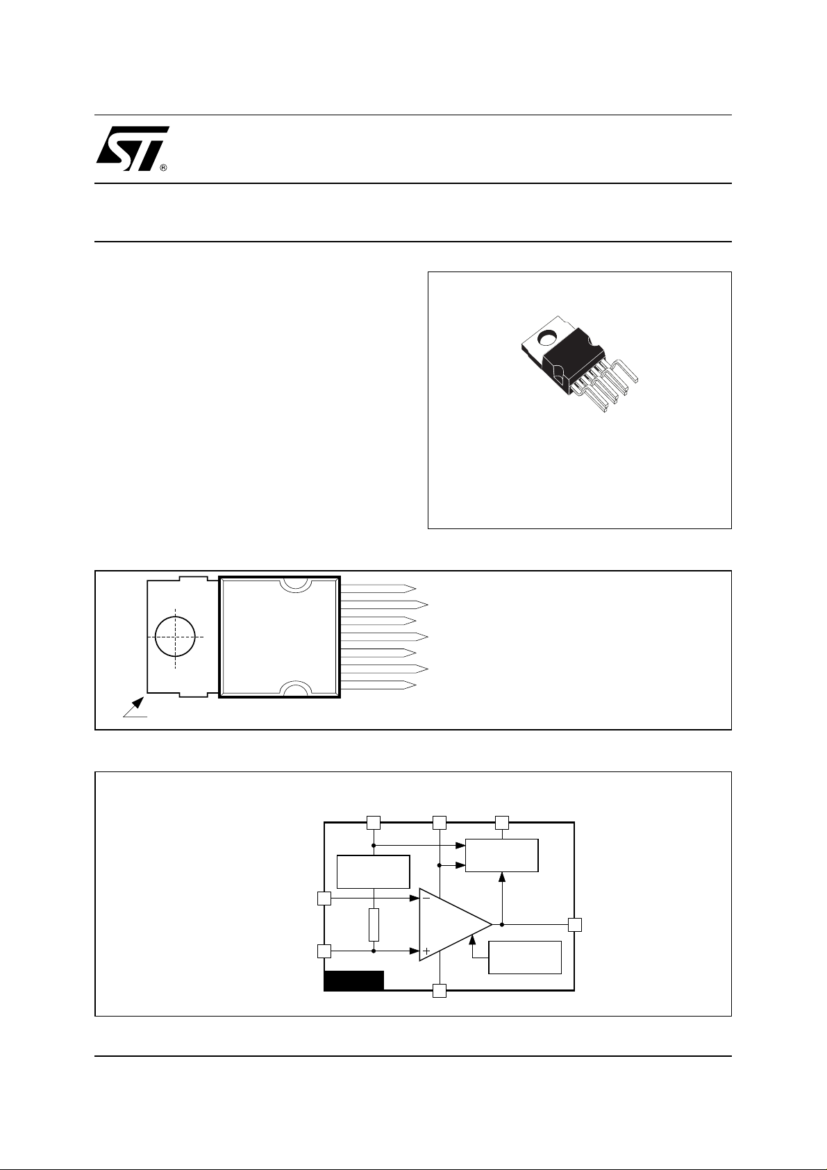
The TDA8171 is offered in HEPT A WATT package.
PIN CONNECTIONS
output curren t to drive the y oke.
PP
PP
HEPTAWATT
(Plastic Package)
ORDER CODE :
TDA8171
TDA8171
Tab connected to Pin 4
BLOCK DIAGRAM
+ REFERENCE VOLTAGE
INVERTING INPUT
NON-INVERTING
7
6
5
4
3
2
1
VOLTAGE
REFERENCE
VOLTAGE
1
10k
7
TDA8171
SUPPLY
2
Ω
NON-INVERTING INPUT + REFERENCE VOLTAGE
OUTPUT STAGE SUPPLY
OUTPUT
GROUND
FLYBACK GENERATOR
SUPPLY VOLTAGE
INVERTING INPUT
OUTPUT
STAGE
SUPPLY
6
POWER
AMPLIFIER
4
GROUND
FLYBACK
GENERATOR
3
FLYBACK
GENERATOR
THERMAL
PROTECTION
5
OUTPUT
8171-01.EPS
8171-02.EPS
December 1998
1/4
TDA8171
ABSOLUTE MAXIMUM RATINGS
Symbol Parameter Value Unit
V
V
, V7Amplifier Input Voltage (Pins 1-7) (see Note 1) - 0.3, + V
V
1
I
V
ESD
T
oper
T
T
Notes :
THERMAL DATA
Symbol Parameter Value Unit
R
th (j-c)
T
T
Supply Voltage (Pin 2) (see Note 1) 40 V
S
Flyback Peak Voltage (Pin 6) (see Note 1) 75 V
6
Maximum Output Peak Current (see Notes 2 and 3) 2.5 A
O
Maximum Sink Current (first part of flyback) (t < 1ms) 2.5 A
I
3
Maximum Source Current (t < 1ms) 2.5 A
I
3
Electrostatic Handling for all pins (see Note 4) 2000 V
Operating Ambient Temperature - 20, + 75
Storage Temperature - 40, + 150
stg
Junction Temperature +150
j
1. Versus Pin 4.
2. The output current can reach 4A peak for t ≤ 10µs (up to 120Hz).
3. Provided SOAR is respected (see Figures 1 and 2).
4. Equivalent to discharging a 100pF capacitor through a 1.5kΩ series resistor.
Junction-case Thermal Resistance Max. 3
Temperature for Thermal Shutdown 150
t
Recommended Max. Junction Temperature 120
jr
S
o
C/W
V
o
C
o
C
o
C
o
C
o
C
8171-01.TBL
8171-02.TBL
ELECTRICAL CHARACTERISTICS
(V
= 35V, TA = 25oC, unless otherwise specified)
S
Symbol Parameter Test Conditions Min. Typ. Max. Unit
V
V
∆
V
7
∆
V
GV Voltage Gain 80 dB
V
V
V
D5 - 6
V
D3 - 2
V
V
Operating Supply Voltage Range 10 35 V
S
Pin 2 Quiescent Current I3 = 0, I5 = 0 9 20 mA
I
2
Pin 6 Quiescent Current I3 = 0, I5 = 0, V6 = 35V 8 15 30 mA
I
6
Max. Peak Output Current 1.5 A
I
O
Amplifier Bias Current V1 = 1V - 1
I
1
Reference Voltage 2.35 V
7
/∆VSReference Voltage Drift versus Supply Voltage 1 2 mV/V
/∆t Reference Voltage Drift versus Temperature 0.15 mV/oC
7
Output Saturation Voltage to GND (Pin 4) I5 = 1.5A 1 1.7 V
5L
Output Saturation Voltage to Supply (Pin 6) I5 = - 1.5A 1.8 2.3 V
5H
Diode Forward Voltage between Pins 5-6 I5 = 1.5A 1.8 2.3 V
Diode Forward Voltage between Pins 3-2 I3 = 1.5A 1.6 2.2 V
Saturation Voltage on Pin 3 I3 = 20mA 0.4 1 V
3SL
Saturation Voltage to Pin 2 (2nd part of flyback) I3 = - 1.5A 2.1 2.8 V
3SH
µ
A
8171-03.TBL
2/4
 Loading...