


TV VERTICALDEFLECTION OUTPUT CIRCUIT
The functionsincorporatedare :
.
POWERAMPLIFIER
.
FLYBACKGENERATOR
.
REFERENCE VOLTAGE
.
THERMALPROTECTION
DESCRIPTION
The TDA8170 is a monolithic integrated circuit in
HEPTAWATT
powerboosterfor directdrivingof verticalwindings
of TV yokes. It is intended for use in Colour and B
&W televisionreceiversaswell asin monitorsand
displays.
PIN CONNECTIONS
TM
package. It is a high efficiency
TDA8170
HEPTAWATT
(PlasticPackage)
ORDER CODE : TDA8170
Tab connected to Pin 4
BLOCKDIAGRAM
7
6
5
4
3
2
1
236
REFERENCE
VOLTAGE
1
7
TDA8170
POWER
AMPLIFIER
4
REFERENCEVOLTAGE AND NON-INVERTING INPUT
OUTPUT STAGE SUPPLY
OUTPUT
GROUND
FLYBACK GENERATOR
SUPPLY VOLTAGE
INVERTING INPUT
+V
S
FLYBACK
GENER ATOR
5
THERMAL
PROTEC TION
YOKE
8170-01.EPS
December 1997
8170-02.EPS
1/7
TDA8170
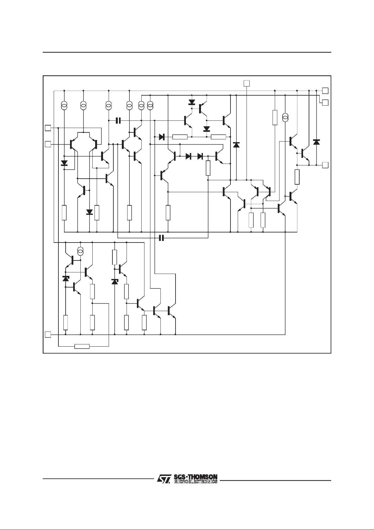
SCHEMATIC DIAGRAM
5
2
D4
C1
7
1
Q23
D1
R1
Z1
Q1 Q2
Q3
D2
Q25
Q4
Q5
R2
R12
Q24
Z2
R13
Q7
Q6
Q8
R3
Q26
R14
Q27
D3
R4
Q9
Q14
R7
C2
Q28
Q29
Q11
Q10 Q12
D5
D6 D7
R5
Q13
R6
Q15
D8
Q17
Q16
R8 R9
R10
Q18
Q20
R11
Q22
Q19
6
D9
Q21
3
2/7
R16
4
R19
R17
R18R15
8170-03.EPS

TDA8170
ABSOLUTE MAXIMUMRATINGS
Symbol Parameter Value Unit
V
V
5,V6
V
V1,V7Amplifier Input Voltage + Vs, – 0.5 V
P
T
stg,Tj
THERMAL DATA
Symbol Parameter Value Unit
R
th j–case
Supply Voltage (pin 2) 35 V
S
Flyback Peak Voltage 60 V
Voltage at Pin 3 + V
3
Output Peak Current (non repetitive, t = 2 msec) 2.5 A
I
o
Output Peak Current at f = 50 or 60 Hz, t ≤ 10 µsec 3 A
I
o
Output Peak Current at f = 50 or 60 Hz, t > 10 µsec 2 A
I
o
Pin 3 DC Current at V5<V
I
3
Pin 3 Peak to Peak Flyback Current at f= 50 or 60 Hz, t
I
3
Total Power Dissipation at T
tot
2
≤1.5msec 3 A
fly
=90°C20W
case
s
100 mA
Storage and Junction Temperature – 40, +150
Thermal Resistance Junction-case Max. 3 °C/W
C
°
8170-01.TBL
8170-02.TBL
ELECTRICAL CHARACTERISTICS
(refer to the test circuits, V
= 35V, T
S
Symbol Parameter Test Conditions Min. Typ. Max. Unit Fig.
Pin 2 Quiescent Current I3=0,I5=0 8 16 mA 1a
I
2
Pin 6 Quiescent Current I3=0,I5= 0 16 36 mA 1a
I
6
Amplifier Input Bias Current V1= 1 V – 0.1 – 1 µA1a
I
1
V
∆V
∆
V
V
V
V
T
Reference Voltage 2.2 V 1a
7
7
Reference Voltage Drift versus Supply Voltage Vs= 15 to 30 V 1 2 mV/V 1a
V
S
Pin 3 Saturation Voltage to GND I3=20mA 1 V 1c
3L
Quiescent Output Voltage Vs=35V,Ra=39k
5
Output SaturationVoltage to GND I5= 1.2 A 1 1.4 V 1c
5L
Output SaturationVoltage to Supply – I5= 1.2 A 1.6 2.2 V 1b
5H
Junction Temperature for Thermal Shut Down 140 °C
j
=25oC unlessotherwisespecified)
amb
=15V,Ra=13kΩ 7.5 V 1d
V
s
= 0.7 A 0.7 1 V 1c
I
5
= 0.7 A 1.3 1.8 V 1b
–I
5
Ω
18 V 1d
8170-03.TBL
3/7

TDA8170
Figure1a : Measurementof I1,I2,I6,V7,
∆V
/∆V
7
S
+V
S
I
2
2
TDA8170
7
V
7
S1 : (a)I2and I6; (b) I
1
Figure1c : Measurementof V3L,V
2
1
3V
TDA8170
I
6
6
5
10kΩ
S1
1
4
a
b
I
1
1V
5L
I3or I
6
S1
3
b
5
4
V
3L
Figure1b : Measurementof V
2
1
TDA8170
5H
+V
S
6
V
5H
5
1V
4
8170-04.EPS
Figure1d : Measurementof V
+V
S
5
12kΩ
a
2V
V
5L
5.6kΩ
2
1
TDA8170
R
a
5
6
4
-I
5
8170-05.EPS
+V
S
5
V
5
S1 : (a) V3L; (b) V
5L
Figure2 : Application Schematic
V
S
µF
C7 1
7
4/7
GND
to
V
i
RT1
R1
10kΩ
4.7kΩ
IN
R2
5.6k
1
Ω
8170-06.EPS
1N4001
C2
470µF
D1
2
C1
0.1µF
TDA8170
4
R3 R4
12kΩ 8.2kΩ
C6
4.7
µF
63
C3
220
8170-07.EPS
t
R5 Iy
fly
V
7
to
8170-08.EPS
µF
Iy
5
C4
0.22
R7
1.5
2200
µF
Ω
C5
µF
R5
1
Ω
R6
330
Ly
24.6mH
Ω
Ry
9.6
Ω
to

Figure3 : PC Boardand Componentlayout of the Circuit of fig.2(1 : 1 scale)
TDA8170
C1
C2
C5
R4
R5
R2
GND YOKE
V
S
COMPONENTSLIST FOR TYPICALAPPLICATIONS
Component
RT1 10 4.7 10 kΩ
R1 12 10 12 k
R2 10 5.6 5.6 kΩ
R3 27 12 18 kΩ
R4 12 8.2 5.6 k
R5 0.82 1 1 Ω
R6 270 330 330 Ω
R7 1.5 1.5 1.5
D1 1N 4001 1N 4001 1N 4001 –
C1 0.1 0.1 0.1 µF
C2 eI. 1000/25V 470/25 V 470/25 V
C3 eI. 220/25V 220/25 V 220/25 V µF
C4 0.22 0.22 0.22 µF
C5 eI. 200/25V 2200/25 V 1000/16 V
C6 eI. 4.7/16V 4.7/16 V 10/16 V µF
C7 1.0/16V 1.0/16V 1.0/16V µF
110 ° TVC
5.9 Ω/10 mH
1.95 App
110 ° TVC
9.6 Ω/24.6 mH
1.2 App
D1
R1
R3
R6
YOKE
()
TDA8170
GND
V
O
R7
C6
V
7
90 ° TVC
15 Ω/30 mH
0.82 App
C3
R11
IN
Unit
Ω
Ω
Ω
µ
µ
8170-09.EPS
F
F
8170-04.TBL
5/7

TDA8170
TYPICALPERFORMANCES
Parameter
- Supply Voltage 24 22.5 25 V
V
s
- Current 280 175 125 mA
I
s
- FlybackTime 0.6 1 0.7 ms
t
fly
- Power Dissip. 4.2 2.5 2.05 W
P
tot
- Heatsink 7 13 16
R
tho-a
T
amb
T
j max
T
o
V
I
V
7
110 ° TVC
5.9Ω/10 mH
60 60 60 °C
110 110 110 °C
20 20 20 ms
2.5 2.5 2.5 V
2.5 2.5 2.5 V
MOUNTINGINSTRUCTIONS
The power dissipated in the circuit must be removedby adding an externalheatsink.
Thanks to the HEPTAWATT
TM
package attaching
theheatsinkis very simple,a screwa compression
110 ° TVC
9.6Ω/27 mH
spring(clip)being sufficient.Betweenthe heatsink
andthepackageitisbettertoinsertalayerofsilicon
grease,to optimizethe thermalcontact; no electrical isolation is needed between the two surfaces.
90 ° TVC
15Ω/30 mH
Unit
C/W
°
pp
p
8170-05.TBL
Figure4 : MountingExamples
8170-10.EPS
6/7

PACKAGEMECHANICAL DATA : 7 PINS - PLASTICHEPTAWATT
Dimensions
Min. Typ. Max. Min. Typ. Max.
A 4.8 0.189
C 1.37 0.054
D 2.4 2.8 0.094 0.110
D1 1.2 1.35 0.047 0.053
E 0.35 0.55 0.014 0.022
F 0.6 08 0.024 0.031
F1 0.9 0.035
G 2.41 2.54 2.67 0.095 0.100 0.105
G1 4.91 5.08 5.21 0.193 0.200 0.205
G2 7.49 7.62 7.8 0.295 0.300 0.307
H2 10.4 0.409
H3 10.05 10.4 0.396 0.409
L 16.97 0.668
L1 14.92 0.587
L2 21.54 0.848
L3 22.62 0.891
L5 2.6 3 0.102 0.118
L6 15.1 15.8 0.594 0.622
L7 6 6.6 0.236 0.260
M 2.8 0.110
M1 5.08 0.200
Dia. 3.65 3.85 0.144 0.152
Millimeters Inches
TDA8170
PM-HEPTV.EPS
HEPTV.TBL
Informationfurnished is believedto be accurate and reliable. However, SGS-THOMSON Microelectronicsassumes no responsibility
for the consequences of use of suchinformation nor for any infringement of patents or other rights of third parties which may result
fromitsuse. No licenceis granted by implicationor otherwise under any patent orpatent rights of SGS-THOMSON Microelectronics.
Specifications mentioned in this publication are subject to change without notice. This pu blication supersedes and replaces all
informationpreviously supplied. SGS-THOMSON Microelectronics productsare not authorized for use as critical components in life
support devices or systems without expresswritten approval of SGS-THOMSON Microelectronics.
1997 SGS-THOMSON Microelectronics- All Rights Reserved
Purchase of I2C Components of SGS-THOMSON Microelectronics,conveys a license under the Philips
2
I
C Patent.Rights to use these components in a I2C system,is granted provided that the system conforms to
Australia - Brazil - Canada - China - France- Germany - Italy - Japan - Korea - Malaysia - Malta - Morocco
The Netherlands- Singapore- Spain - Sweden - Switzerland- Taiwan - Thailand- United Kingdom - U.S.A.
2
C Standard Specifications as defined by Philips.
the I
SGS-THOMSON Microelectronics GROUP OF COMPANIES
7/7
 Loading...