

RGB VIDEO OUTPUTAMPLIFIER
.
THREE INDEPENDENT VIDEO AMPLIFIERS
WITHTYPICAL SR > 1000V/µs
.
CRT-CATHODE SENSINGOUTPUT FOR SEQUENTIALSAMPLING
.
INTERNAL G1 VOLTAGEGENERATOR
.
CATHODE SHORTCIRCUITPROTECTION
.
FLASHOVER PROTECTION OF THE OUTPUTSTAGES
.
COMPENSATES POSITIVE AND NEGATIVE
TUBE LEAKAGES
DESCRIPTION
Realizedwitha highvoltagebipolartechnology,the
TDA8153is a monolithic RGB video output stage
for TV color applications. It drives the CRT cathodesdirectlyandoffersa videobandwidthcompatible with CCIR standards. In addition to three
independent video amplifiers, the device features
an internal generator for the first grid voltage,
flashover protection, cathode short circuit protection and a commoncut-off sensing output for use
in sequentialsampling applications.
The TDA8153 is supplied in a 15 lead Multiwatt
plasticpower package.
TDA8153
MULTIWATT15
(Plastic Package)
ORDER CODE : TDA8153
PINCONNECTIONS
January 1993
Tab connected to Pin 8
15
14
13
12
11
10
GREEN OUTPUT
BLUE FEEDBACK
BLUE OUTPUT
CUT-OFF
V
S
V
REF
9
8
7
6
5
4
3
2
1
BLUE INPUT
GROUND
GREEN INPUT
RED INPUT
FIRST GRIDE VOLTAGE
V
H
RED OUTPUT
RED FEEDBACK
GREEN FEEDBACK
8153-01.EPS
1/11

TDA8153
PIN FUNCTIONS
N° Name Function
1 GREEN
FEEDBACK
2 RED FEEDBACK Feedback Output for ’Red’ Amplifier. See pin 1.
3 RED OUTPUT Output of ’Red’ Video Amplifier. See pin 15.
4V
H
5 FIRST GRID
VOLTAGE
6 RED INPUT Input of ’Red’ Video Amplifier. See pin 7.
7 GREEN INPUT Input of ”Green” Video Amplifier. The bias voltage at the inputs is equal to V
8 GROUND Ground Connection(pin 8 is also connected to the tab).
9 BLUE INPUT Input of ’Blue’ Video Amplifier. See pin 7.
10 V
11 V
ref
s
12 SAMPLING Cathode Current Sampling Output. Provides sum of cathode currents for automatic cut-off
13 BLUE OUTPUT Output of ’Blue’ Video Amplifier.See pin 15.
14 BLUE FEEDBACK Feedback Output for ’Blue’ Amplifier. See pin 1.
15 GREEN OUTPUT Output of the ’Green’Video Amplifier.The output is protected against CRT flashovers. Other
Feedback Output for ’Green’ Amplifier. The optimal value for the resistor connected here to set
gain is 68kΩ as shown in fig. 1.2. Other feedback connections are pin2 (red) and pin 14 (blue).
High VoltageSupply for Amplifier Stages, Typically 200V (see fig. 1.2).
Output providing DC voltage for first grid of CRT, typically V
inputs are pin 6 (red) and pin 9 (blue).
s+VBE
.
+2VBE. Other
ref
The reference voltage for thethree amplifiers isavailable on this pin. Typical value is1.6V. The
capacitor connectedbetweenpin 10 andgroundeliminatesAC crosstalk between the amplifiers.
Supply VoltageInput for Low Voltage Circuitry, typically 12V.
adjustment withvideo processors usingthe sequential system. The three currentgenerators I
and I3bias the inputs of this circuit which performs the cut-off adjustment, allowing also
I
2
adjustment with in flowing CRT leakages.
outputs are pin 3 (red) and pin 13 (blue).
,
1
8153-01.TBL
SCHEMATIC DIAGRAM
4
11
6
Q4
Q6
R4 R5
R1
Q1
D2 D3
2
12
Q5
R3
R2
R25
Q2
D4
Q31
7
3
Q10
R9 R10
R6
D5 D6
Q11
Q12
Q7
R26
Q32
R7
D7
15
Q8
1
R9
9
Q16
Q15
R14 R15
R11
Q13
D8 D9
14
R13
Q17
R12
R27
D11
Q14
D10
Q33
I3I2I1 I4
13
5
2/11
10
1.6V
8
8153-02.EPS
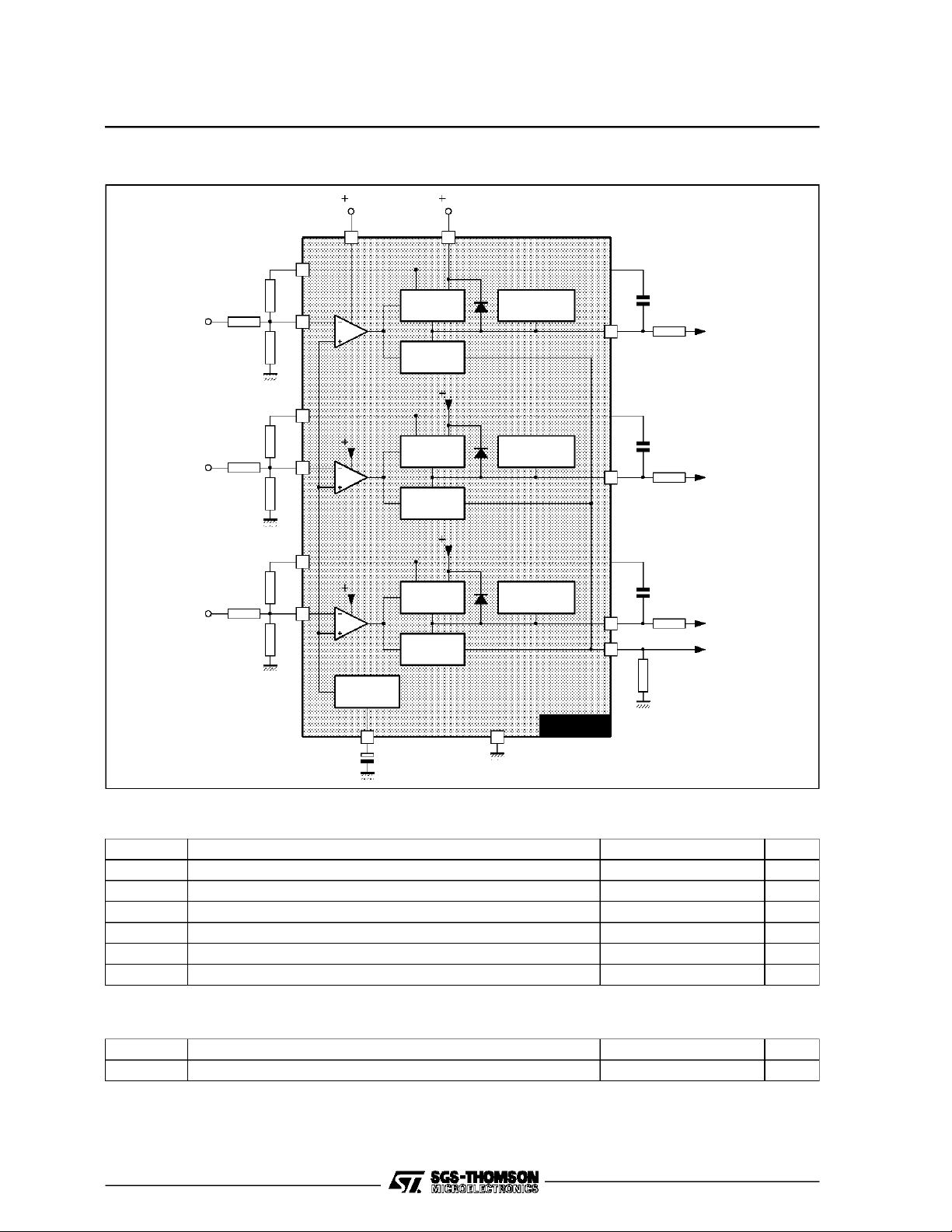
BLOCK DIAGRAM
TDA8153
RED IN
GREEN IN
BLUE IN
V
S
11 4
2
6
1
V
S
7
14
V
S
9
HV
OUTPUT
CUT-OFF
SENSING
HV
OUTPUT
CUT-OFF
SENSING
HV
OUTPUT
CUT-OFF
SENSING
V
H
SHORT CIRCUIT
PROTECT
3
V
H
SHORT CIRCUIT
PROTECT
15
V
H
SHORT CIRCUIT
PROTECT
13
12
RED OUT
GREEN OUT
BLUE OUT
CUT-OFF
SAMPLING
REFERENCE
VOLTAGE
10 8
TDA8153
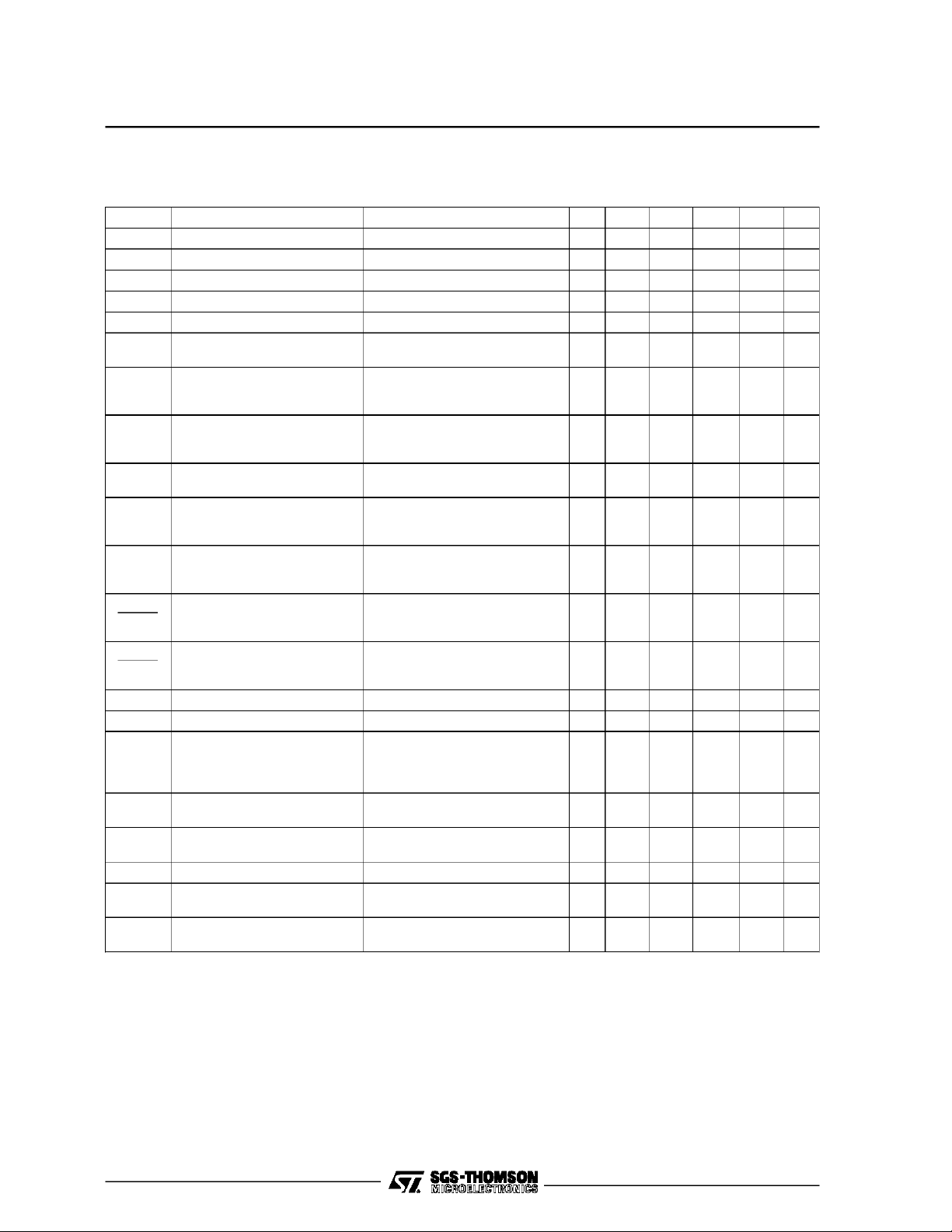
ABSOLUTEMAXIMUM RATINGS
Symbol Parameter Value Unit
V
H
V
S
P
tot
V
T
stg,Tj
T
oper
High VoltageSupply 250 V
Low VoltageSupply 35 V
Power Dissipation at T
Input Voltage V
I
=90°C20W
case
s
Storage and Junction Temperature – 25, + 150 °C
Operating Ambient Temperature 0, + 70 °C
THERMALDATA
Symbol Parameter Value Unit
R
th (j-c)
Thermal Resistance Junction-case Max 3 °C/W
8153-03.EPS
8153-02.TBL
8153-03.TBL
3/11
TDA8153
ELECTRICALCHARACTERISTICS (ref. to test andapplicationcircuits, VHT= 200V, VS= 12V,
=10pF *, heatsink Rth=9oC/W, T
C
L
Symbol Parameter Test Conditions Pin Min. Typ. Max. Unit Fig.
V
V
I
High Voltage Supply 4 200 220 V 1-2
HT
Low Voltage Supply 11 10.8 12 13.2 V 1-2
S
Quiescent Drain Current Vin = 0, Vodc = Vsat H 4 10 15 mA 1
HT
Quiescent Drain Current Vin = 0, Vodc = Vsat H 11 10 17 mA 1
I
S
Vref ReferenceVoltage 10 1.4 1.6 1.9 V 1
Vg1 CRT G1 Voltage Supply 5 V
Vsat H Output Saturation Vin = 0, Vdc = – 3V 3
Vsat L Output Saturation Vin = 0, Vdc = 9V 3
I1,I2,I
3
Vodc Quiescent Output Voltage Inputs Floating 3
Vo Peak-to-peakOutput Swing f = 10KHz 3
∆Vodc∆TDC Output Voltage versus
Temperature Vodc = 150V
∆Vodc∆TDC Differential Voltage
versus Temperature
GVo Open-loop Gain Vin = 50mVpp, f = 10kHz 50 56 dB 1
GVc Closed-loop Gain Vin = 1.5Vpp, f = 10kHz 20 25 dB 1
Bw Video Bandwidth (–3 dB) Vobl = 125V, 0dB at f = 100kHz
tr Rise Time Vo= 100Vpp; Vobl = 150V
tf Fall Time Vo= 100Vpp; Vobl = 150V
∆T DifferentialRise and Fall Time 20 ns 2
Overshoot Vo= 100Vpp, Vobl= 150V
Undershoot Vo = 100Vpp ;Vobl =150V
* CL = 10pF is the sum of the P.C. board capacitance (with socket) and the cathode capacitance of the CRT.
=25oCunless otherwise specified)
amb
See schematic diagr.
Vin = 0 ; Vodc = 150V
Tamb = 0 ÷ 70°C
Vodc = 150V
Tamb = 0 ÷ 70°C
Vo = 80Vpp
50Vpp
10Vpp
f = 100kHz, Duty Cycle = 0.5
f = 100kHz, Duty Cycle = 0.5
f = 100kHz, Duty Cycle = 0.5
f = 100kHz, Duty Cycle = 0.5
13
s
Vbe
V
HT
–3V
+
V1
V1
15
13
V
s
V1
15
12 7 15 20 µA1
123 V 1
13
15
170 Vpp 1
13
15
3
13
0.03 V/°C1
15
3
0.015 V/°C1
13
15
4.5
6.5
12
6.0
8.0
15
MHz 2
80 120 ns 2
80 120 ns 2
5%2
5%2
8153-04.TBL
4/11

TEST CIRCUIT
TDA8153
Vin
VDC
CUT-OFF
GND
BIN
GIN
RIN
R6
R7
R8
R9
+VHT
+VS
R3
R10
R4
R1
R11
C1
R5
R12
R2
4
11
2
1
14
9
7
6
12
8
10
C3
C2
R16
5
R13
13
R14
15
R15
3
VG1
B OUT
CL
G OUT
CL
R OUT
CL
8153-04.EPS
5/11

TDA8153
TEST CIRCUIT
R1 = 10Ω
R2 = 220Ω 1/2W
R3 = 68kΩ 1/2W
R4 = 68kΩ 1/2W
R5 = 68kΩ 1/2W
R6 = 3kΩ
R7 = 3kΩ
R8 = 3kΩ
GREENIN
BLUE IN
+VS
GND
R7
R11
R12
R6
R4
R5
R1
+
C1
R9 = 47kΩ
R10 = 1.8kΩ 1/2W
R11 = 1.8kΩ 1/2W
R12 = 1.8kΩ 1/2W
R13=1kΩ 1/2W
R14=1kΩ 1/2W
R15=1kΩ 1/2W
R16 = 2.2kΩ
CUT
OFF
R2
R16
R15
R3
C2
+
R9
R8
R10
C3
R14
R13
+VHT
VG1
RED OUT
RED IN
GREENOUT
BLUEOUT
C1 = 4µF 16V
C2 = 100nF 250V
C3 = 10µF 16V
8153-05.TIF/ 8153-06.EPS
6/11

APPLICATION CIRCUIT
TDA8153
EHT
G3
C5
1kV
2.2nF
G1
Ω
2W
R18
10k
Ω
2W
R17
Ω
-1/2W
Ω
-1/2W
Ω
-1/2W
Ω
0.1
G2
HG
C2
C1
R3
R16 2.2k
5
1
R5
68kΩ
1/2W
R4
68kΩ1/2W
68kΩ
1/2W
R13 1k
131415
9
R14 1k
R15 1k
3
8
C4
10µF
16V
10
7
6
12
R12
1.8kΩ
R11
1.8kΩ
R10
1.8kΩ
Ω
C3
0.1µF
250V
4
11
3
15
13
2
C11
100pF
C10
100pF
C9
100pF
0.1µF
16V
47µF
R2 220Ω-1W
+VHT
C13 39pF C7 22pF
P2 R7 2.2kΩ
R9 680Ω R8 2.2kΩ
C14 68pF C8 22pF
GIN
RIN
CUT-OFF
GND
8153-07.EPS
P1 R6 2.2k
R1 10Ω
+VS
C12 68pF C6 22pF
BIN
7/11

TDA8153
APPLICATION CIRCUIT
+VHT
F
GND
GND
R17
C5
R18
G2
C14
RED IN
C9
R14
R13
R9
C4
R10
R3
R15
R16
R2
+
CUT
OFF
C3
C9
C11
C2C1
+
R1
C12
C10
C6
C13
GND
+VS
BLUE IN
P1
C7
R7
R11
R12
R6
P2
GREEN IN
8153-08.TIF / 8153-09.EPS
8/11

Figure2 : Fall Time
Figure 1 : VideoBandwith
G(dB)
+1
0
V
=80V
O
-1
V
OBL
-2
-3
-4
-5
-6
-7
-8
-9
100k 1M 10M
PP
= 125V
f(MHz)
Figure3 : Rise Time
TDA8153
8153-10.EPS
90%
50ns/div. ; uncal
10%
APPLICATION NOTES
P. C. Board
The best performance of the RGB video amplifier
canbe obtainedonlywith acarefullydesignedP.C.
board. The layout of the printed circuit must be
realizedto achieve the best possible symmetry of
the three channels.
Output to input capacitances are of particular importance.The input-outputcapacitances,in parallel with the relative high feedback resistances,
createpoles in the closedloop transfer function.
To optimizethe band responseandto minimizethe
channels crosstalk a low parasitic capacitance
feedback resistors of not inductive type is necessary.
Capacitivecouplingfromthe output of an amplifier
and theinput ofanother onemayinduceexcessive
crosstalk.It is advisableto keep the amplifier outputs away from amplifier inputs.
The small size of the P.C. board allows you to
90%
50 ns/div.; uncal
10%
8153-11.EPS
mounttheTDA8153directlybesidethepicturetube
socket, to minimize the capacitances of the connectionsbetween the video amplifiersand the picture tube cathodes.
The capacitors connectedin parallel with the input
resistorscompensate the effects of the distributed
constantsofthe printedcircuitonthe stepresponse
times. Their values must be selected on the basis
of the layout and can be consideredas function of
the printedcircuit.
The three capacitors (C9, C10, C11) between the
amplifier outputs and the feedback resistors reduces the noise effect on the cut-off control, their
value, of course, depends on the noise amplitude
and spectrumcoming from theI.F. video stage.
To prevent possible oscillationproblems, it is necessarytoplacethe highvoltagefiltercapacitor(C3)
as nearas possibleto the IC groundand the latter
must be of a substantialwidth.
8153-12.EPS
9/11

TDA8153
Power Dissipation
Taking as reference the IC internalschematic diagram wecan calculatethe powerdissipatedby the
videoamplifiers.
ThepowerdissipationoftheICis definedbya static
an a dynamic part.
The staticallydissipated poweris given by :
PS= 3V
ht
Vht− V
R1
obl
V
obl
+
R
f
− 3
2
V
R
obl
(V
ref
− 3
f
+ 2Vbe)
R
b
2
Where Rfis the feedback resistance and Rb the
input to ground resistance with a black level
=150V,Vht=200V,Rf=68kΩ andRb=1.8kΩ
V
obl
we have : P
=1.75W
S
The dynamic power dissipation has been calculatedwith a 5MHz, 80Vpp sinusoidaloutput signal
and a load capacitor C
expression:
Pd=
0.8 Vht(2f C
= 10pF with the following
L
2
V
op
LVop
) − 0.8
2R
= 1.90W
f
The value is reducedby 20% (0.8factor) because
duringthe flybacktime there is not signal.
The total power dissipated by the IC is therefore :
PT=PS+Pd= 1.75 + 1.90 = 3.65W
One ofthe worst workingconditionof theTVsetas
regards the power dissipation, is when you get
white noise on the screen,for example, when you
disconnect the TV aerial or the channels are not
properlytuned.
In these casesif we set the TVreceiver for 80V
PP
white noise output signal with a black level
= 125V, the total power dissipated by the IC
V
ob1
canbe measured.
It resultsabout P
= 4.8W.
T
Witha maximumambient temperatureof 70°Cand
ajunction temperatureof 150°Ca15°C/Wheatsink
isrequired.
Figure4 : MaximumAllowable Power Dissipation
versus AmbientTemperature
8153-13.EPS
Figure5 : MountingExamples
8153-14.EPS / 8153-15.EPS
10/11

TDA8153
PACKAGE MECHANICALDATA: 15 PINS - PLASTIC MULTIWATT
Dimensions
Min. Typ. Max. Min. Typ. Max.
A 5 0.197
B 2.65 0.104
C 1.6 0.063
D 1 0.039
E 0.49 0.55 0.019 0.022
F 0.66 0.75 0.026 0.030
G 1.14 1.27 1.4 0.045 0.050 0.055
G1 17.57 17.78 17.91 0.692 0.700 0.705
H1 19.6 0.772
H2 20.2 0.795
L 22.1 22.6 0.870 0.890
L1 22 22.5 0.866 0.886
L2 17.65 18.1 0.695 0.713
L3 17.25 17.5 17.75 0.679 0.689 0.699
L4 10.3 10.7 10.9 0.406 0.421 0.429
L7 2.65 2.9 0.104 0.114
M 4.2 4.3 4.6 0.165 0.169 0.181
M1 4.5 5.08 5.3 0.177 0.200 0.209
S 1.9 2.6 0.075 0.102
S1 1.9 2.6 0.075 0.102
Dia. 1 3.65 3.85 0.144 0.152
Information furnished is believed to be accurate and reliable. However,SGS-THOMSON Microelectronics assumes no responsibility
for the consequences of use of suchinformation nor forany infringement of patents or other rights of third parties which may result
from its use. No licence is granted by implication or otherwiseunder any patent or patent rights ofSGS-THOMSON Microelectronics.
Specifications mentioned in this publication are subject to change without notice. This publication supersedes and replaces all
information previously supplied.SGS-THOMSON Microelectronics products are not authorized for use as critical components in life
support devices or systems without express written approval of SGS-THOMSON Microelectronics.
Millimeters Inches
PMMUL15V.EPS
MUL15V.TBL
1994 SGS-THOMSON Microelectronics - All Rights Reserved
Purchase of I2C Components of SGS-THOMSON Microelectronics, conveys a license under the Philips
2
I
C Patent.Rights to usethese components in a I2C system, is granted provided that the system conforms to
Australia - Brazil - China - France - Germany- Hong Kong - Italy - Japan - Korea - Malaysia - Malta - Morocco
The Netherlands - Singapore -Spain - Sweden - Switzerland - Taiwan - Thailand - United Kingdom - U.S.A.
2
the I
C Standard Specifications as defined by Philips.
SGS-THOMSON Microelectronics GROUP OF COMPANIES
11/11
 Loading...