

SGS Thomson Microelectronics TDA8146 Datasheet

.
LOW POW E R DIS SI PATIO N
.
PULSE WIDTH MODULATOR FOR SWITCH
MODE OPE R ATION
.
OUTPUT SINK CURRE NT UP TO 800mA
.
OUTPUT SOUR CE CURRE NT UP T O 100mA
.
PARASITIC PARABOLA SUPPRESSION
DURING VERTICAL FLYBACK
.
VERTICAL CURRENT SENSE INPUTS
GROUND COMPATIBLE
.
PROGRAMMABLE PARABOLA CURRENT
GENERATOR FOR DIFFERENT TV-TUBES
.
EXTERNAL KEYSTONE ADJUSTMENT
DESCRIPTION
The TDA8146 is a monolithic integrated circuit in a
14 pin dual-in-line plastic package.
The TDA8146 is des igned for use in th e east-wes t
pin-cushion correction by dr iving a diode modulator
in TV and monitor applications.
Since the parabola current generator is programmable the device can operate with different CRTs.
TDA8146
EAST/W EST CORRECT ION
FOR RECTANGU LAR TV-TUBES
DIP14
(Plastic Package)
ORDER CODE : TDA8146
PIN CONN E CTI O NS
May 1993
NOT USED
IGND
IREF
GND
OUT
1
IV
2
3
4
V
5
6
7
14
13
12
11
10
P4
P5
PAR
C
PW
9
Z
8
V
S
8146-01.EPS
1/5
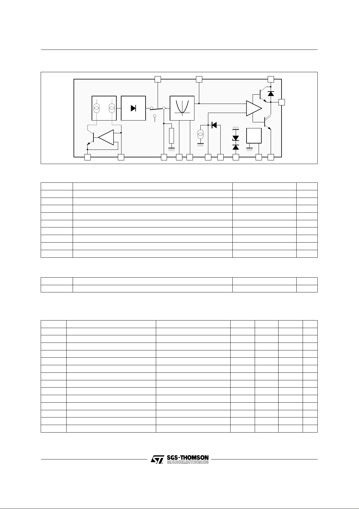
TDA8146
BLOCK DIAGRAM
4
∆
I
I
REF
REF
2.2V
60µA
2
13
14 13
11
10
9
5
812
7
8.2V
6
ABSOLUTE MAXIMUM RATINGS
Symbol Parameter Value Unit
I
7
I
7
V
S
V
4
V
10
V
9
V
in
T
stg
T
Output Sink Current 800 mA
Output Source Current 100 mA
Supply Voltage 33 V
Vertical Flyback Input Voltage – 0.3 to 60 V
Input Voltage at Pin 10 – 10 to V
Input Voltage at Pin 9 – 10 to 20 V
Input Voltage at all other Pins – 0.3 to V
Storage Temperature – 40 to 150 °C
Junction Temperature 0 to 150 °C
j
S
S
8146-02.EPS
V
V
8146-01.TBL
THERMAL DATA
Symbol Parameter Value Unit
R
th (j-a)
Junction-ambient Thermal Resistance Max. 80 °C/W
ELECTRICAL CHARACT E RIS TICS
(refer to test circuit V
Symbol Parameter Test Conditions Min. Typ. Max. Unit
Supply Voltage 15 24 29 V
S
I
Supply Current V
S
Reference Voltage 8.2 V
5
Saturation Voltage IO = 800mA Sink 1.2 2 V
7L
Diode Forward Voltage IO = – 800mA 1.1 1.7 V
SAT
Saturation Voltage IO = 100mA Source 0.8 1.25 V
7H
Current Sink Pin 11 40 60 80 µA
11
Zener Voltage I9 = 5mA 20 22 24 V
9
Vertical Blanking Threshold Voltage VS – 0.5 V
4T
Vertical Blanking Input Current V4 = 50V 25 50 100 µA
I
4
Reference Voltage at Pin 2 R1 = R2 = 10K 1.3 V
2
Reference Voltage at Pin 3 1.3 V
3
Parabola Voltage at Pin 12 ∆ VSE = 0 9.7 V
Parabola Voltage at Pin 12 ∆ VSE = + 0.8V 7.05 V
C
V
V
V
V
V
V
I
V
V
V
V
PARO
V
= 24V, Tj = 25oC ; unless otherwise specified)
S
= LOW 4 7 mA
out
S
VS + 0.5 V
8146-02.TBL
8146-03.TBL
2/5
 Loading...