HORIZONTAL DEFLECTION POWER DRIVER
.
CONTROLLED DRIVING OF THE POWER
TRANSISTOR DURING TURN ON AND OFF
PHASE FOR MINIMUM POWER DISSIPATION AND HIGH RELIAB I LITY
.
HIGH SOURCE AND SINK CURRENT CAPABILITY
.
DISCHARGE CURRENT DERIVED FROM
PEAK CHARGE CURRENT
.
CONTROLLED DIS CHARGE TIMING
.
DISABLE FUNCTION FOR SUPPLY UNDER
VOLTAGE AND NONSYNCHRONOUS OPERATION
.
PROTECTION FUNCTION WITH HYSTERESIS FOR OVERTEMPERATURE
.
OUTPUT DIODE CLAMPING
.
LIMITING OF THE COLLEC TOR PEAK CURRENT OF THE DEFLECTION POWER TRANSISTOR DURI NG TURN ON PERI O D
.
SPECIAL REMOTE FUNCTION WITH DELAY
TIME TO SWITCH THE OUTPUT ON
TDA8143
SIP9
(Plastic Package)
ORDER CODE : TDA8143
DESCRIPTION
The TDA8143 is a monolithic integrated circuit
designed to drive the horizontal deflection power
tran-sistor.
The current source characteristic of this device is
adapted to the non-linear current gain behaviour of
the power transistor providing a minimum power
dissipation. The TDA8143 is internally protected
against short circuits and thermal overload.
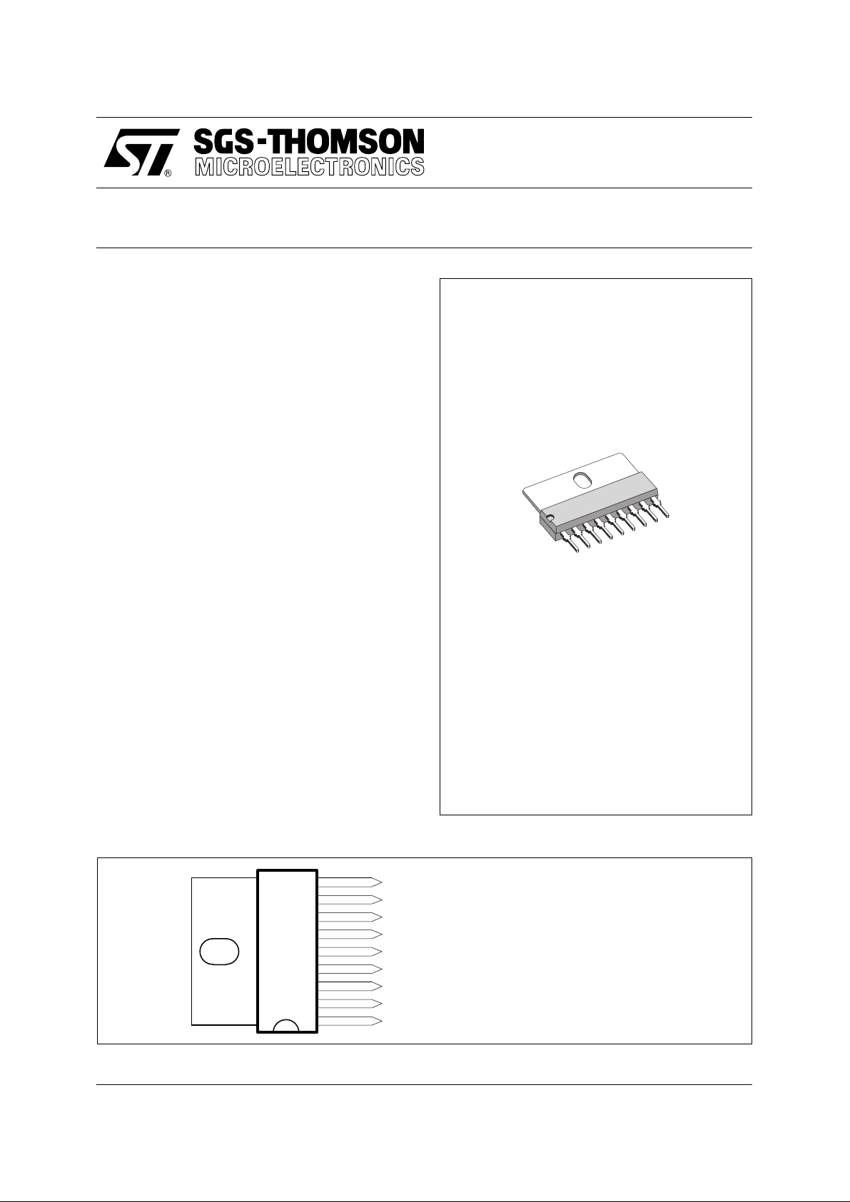
PIN CONNECTIONS
9
8
7
6
5
4
3
2
1
September 1993
PROTECTION AND REMOTE STANDBY INPUT
CONTROL INPUT
SPECIAL REMOTE STANDBY
C
GROUND
SENSE-IN
V+
OUTPUT
GROUND
T
CC
8143-01.EPS
1/9

TDA8143
PIN FUN CTI O NS
Pin Name Function
1 Power Ground Common Ground
2 Ouptut Device Output
3V
CC
4 Sense Input Input voltage that determines output current.
5 Sense GND Reference Ground for Input Voltage at SENSE INPUT.
6C
EXT
7 Special Remote/Standby Low level at this input sets the device after a delay time t
8 Control Input High level at this input switches the BU508 off, low level switches the BU508 on.
9 Protection and Remote
Standby Input
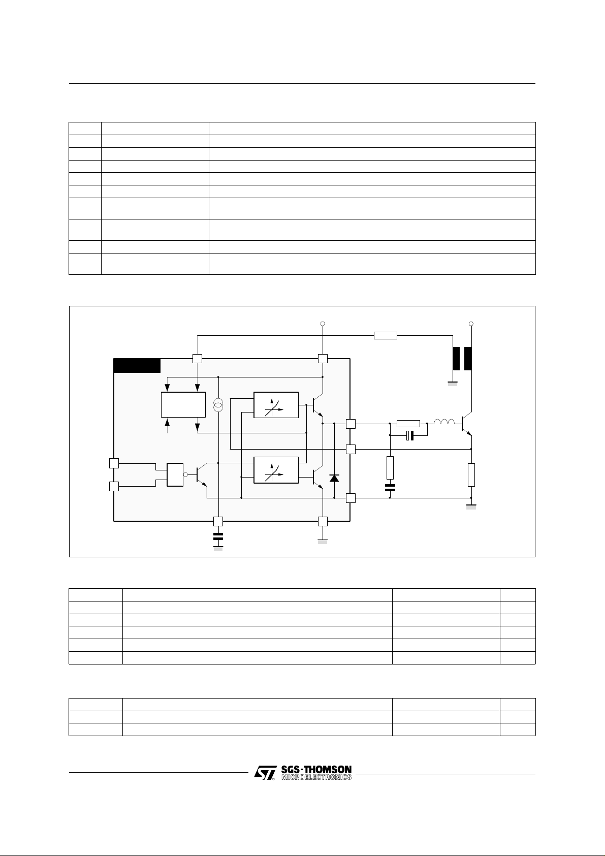
BLOCK DIAG RAM
Supply Voltage
Capacitor between this terminal and SENSE GROUND determines the current
slope dIO/dt during OFF phase.
in the standby mode
independent from CONTROL INPUT (2nd priority).
dr
A high level at this input switches the BU508 off independent from all other inputs
(1st priority).
8143-01.TBL
V
H
BU508
R
0.15
S
Ω
TDA8143
SPECIAL
REMOTE
STANDBY
7
8
CONTROL
IN
SYNC. DET.
THERMAL
PROTECTION
&
PROT ECTION AND
REMOTE ST AN BY INPUT
9
6
C
1nF
VCC+
100k
Ω
3
I
B1
V
S
2
OUT
4
SENSE
I
B2
V
C
1
IN
5
GND
27
220µF
4.7
22nF
Ω
10µH
Ω
ABSOLUTE MAXIMUM RATINGS
Symbol Parameter Value Unit
V
CC
I
d
P
tot
, T
T
stg
T
oper
DC Supply Voltage 18 V
Output Current Internally Limited
Power Dissipation Internally Limited
Storage and Junction Temperature – 40, + 150 °C
j
Operating Temperature 0, + 70 °C
8143-02.EPS
8143-02.TBL
THERMAL DATA
Symbol Parameter Value Unit
Thermal Resistance Junction-ambient Max. 70 °C/W
Thermal Resistance Junction–case Max. 10 °C/W
2/9
R
R
th (j–a)
th (j–c)
8143-03.TBL

TDA8143
ELECTRICAL CHARACTERISTICS (VCC = 12 V, T
= 25oC unless otherwise specified)
amb
Symbol Parameter Test Conditions Min. Typ. Max. Unit
V
CC
I
Q
I
p0
I
n0
I
o0
Supply Voltage 7 18 V
Quiescent Current All Inputs Open 10 15 25 mA
Positive Output Current (source) 1.5 A
Negative Output Current (sink) 2 A
Positive quiescent output current forcing
the output to 6 V and the sense input to
Remote Input1
Remote Input0
120
50
150
80
200
100
ground output externally forced to 6 V.
G
ON
G
OFF
G
REMOTE
I
5
R
INS
I
INS
R
SYN
V
THS
V
SYN
V
THA
I
INA
V
THB
I
INB
t
dr
t
don
V
CC–VOUT
V
CC ON
V
CC OFF
V
S limit
Notes : 1. GON is measured with V4 varying from 150mV to 350mV (Pin 6 is grounded)
Transconductance ON Phase (1) See Figure 1 1.8 2.0 2.2 A/V
Transconductance OFF Phase (2) See Figure 1 1.8 2.0 2.2 A/V
Transconductance Standby Mode Remote Input0 0.675 0.75 0.825 A/V
Current Source Pin 6 V7 = 500 mV 135 165 200 µA
Sense Input Resistance VS > 0
< 0
V
S
0.7
0.35
1
0.5
1.3
0.7
Sense Input Bias Current VS = 0
Remote Input = 1 – 200 – 300 – 400 µA
Synchronous Detection Input Resistance V
Threshold Voltage of the Synchronous
V
SYN
SYN
< 7 V
> 7 V
30
7
60
10
150
15
1 1.8 2.8 V
Detection Input
SYNC DETECT Input Voltage 30 V
Threshold Voltage of Control Input 1.5 2 2.5 V
Pull up Current of Control Input 0 < VIN < V
VIN > V
THA
THA
+ 0.5 V
– 50
– 1
– 1000– 160
+ 1
Threshold Voltage Remote Input 1.5 2 2.5 V
Pull-up Current of the Remote Input 0 < VIN < V
VIN > V
THB
THB
+ 0.5 V
– 50
– 1
– 1000– 160
+ 1
Remote Delay Time (3) 190 250 300 µs
On Delay Time 3 4.5 µs
Output Voltage Drop for Ip0 = 1 A 2 2.8 3 V
Supply Voltage for Device "ON" I0 ≥ 0 5.8 6.4 7.0 V
Supply Voltage for Device "OFF"
(output internally switched to ground)
5.6 V
CC ON
– 0.2 V
6.8 V
Sense Limit Voltage (4) 0.8 0.9 1 V
2. G
is measured with V6 varying from 150mV to 350mV (Pin 4 is grounded)
OFF
3. When the remote input goes from HIGH to LOW the BU508 is switched off and it remains in this condition for the time tdr.
4. The sense input voltage V
the storage time tS of the BU508 limiting of VS leads to a reduced base current of the BU508 and the output current I0 is going to
the positive quiescent current Io0.
is internally limited and results in a limited positive output current Ip0 = g. VS limit. Note that due to
S
mA
mA
kΩ
kΩ
kΩ
kΩ
µA
µA
µA
µA
8143-04.TBL
TRUTH TABLE
Logics Inputs
Control Input Remote/Standby
0
Floating or 1
Floating or 1
Floating or 1
X0 I
X0 I
Note : 5. IO < 0 means that the sink current flows into the output to ground.
> 0
I
0
I0 < 0 (5)
< 0 (5)
0
0 < t < t
> 0
0
t > t
dr
dr
Output I
BU508 ON
BU508 OFF
BU508 OFF
BU508 ON
0
Mode
Normal Function
Remote/Standby
Function
8143-05.TBL
3/9
 Loading...