

TDA8140
HORIZONTAL DEFLECTION POWER DRIVER
.
CONTROLLED DRIVING OF THE POWER
TRANSISTOR DURING TURN ON AND OFF
PHASE FOR MINIMUM POWER DISSIPATION AND HIGH RELIAB I LITY
.
HIGH SOURCE AND SINK CURRENT CAPABILITY
.
DISCHARGE CURRENT DERIVED FROM
PEAK CHARGE CURRENT
.
CONTROLLED DIS CHARGE TIMING
.
DISABLE FUNCTION FOR SUPPLY UNDER
VOLTAGE AND NONSYNCHRONOUS OPERATION
.
PROTECTION FUNCTION WITH HYSTERESIS FOR OVERTEMPERATURE
.
OUTPUT DIODE CLAMPING
.
LIMITING OF THE COLLEC TOR PEAK CURRENT OF THE DEFLECTION POWER TRANSISTOR DURI NG TURN ON PERI O D
.
SPECIAL REMOTE FUNCTION WITH DELAY
TIME TO SWITCH THE OUTPUT ON
The current source characteristic of this device is
adapted to the on-linear current gain behaviour of
the power transistor providing a minimum power
dissipation. The TDA8140 is internally protected
against short circuit and thermal overload.
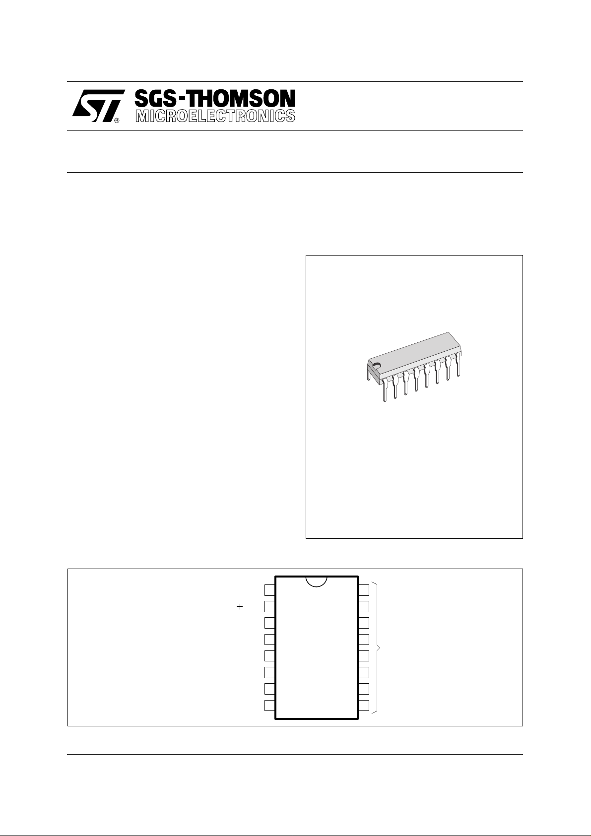
POWERDIP (8 + 8)
(Plastic Package)
ORDER CODE : TDA8140
DESCRIPTION
The TDA 8140 is a mo nolithic integrated cir cuit designed to drive the horizontal deflection power transistor .
PIN CONNECTIONS
OUTPUT
V
CC
SENSE IN
SENSE GND
C
EXT
SPECIAL REMOTE STANDBY
CONTROL INPUT
PROTECTION AND REMOTE
September 1993
STANDBY INPUT
1
2
3
4
5
6
7
8
16
15
14
13
COMMON GND
12
11
10
9
8140-01.EPS
1/10
TDA8140
PIN FUN CTI O N
Pin Name Function
1 Output Device Output
2V
CC
3 Sense Input Input voltage that determines output current.
4 Sense GND Reference Ground for Input Voltage at Sense Input
5C
EXT
6 Special Remote/Standby Low level at this input sets the device after a delay time t
7 Control Input High level at this input switches the BU508 off, low level switches
8 Protection and Remote Standby
Input
9-16 Power Ground Common Ground
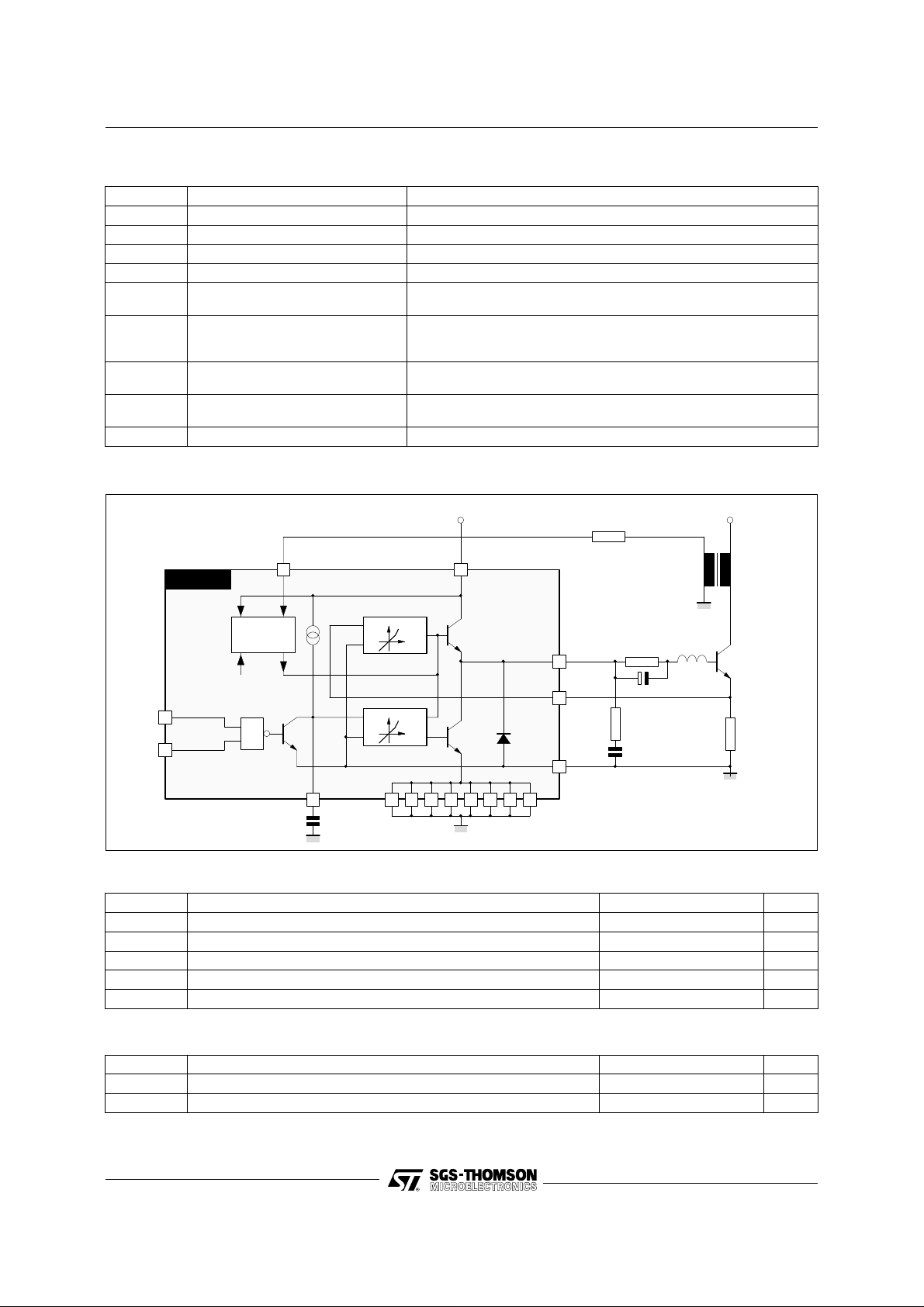
BLOCK DIAG RAM
PROT ECTION AND
REMOTE ST ANBY IN P UT
TDA8140
82
Supply Voltage
Capacitor between this terminal and Sense Ground determines the
current slope dIo/dt during off phase.
standby mode independent from control input (2nd priority) (in
standard applications pin 6 must be left unconnected).
the BU508 on.
A high level at this input switches the BU508 off independent from
all other inputs (1st priority).
VCC+
100k
Ω
in the
dr
8140-01.TBL
V
H
SPECIAL
REMOTE
STANDBY
6
7
CONTROL
SYNC. DET.
THERMAL
PROTECTION
&
IN
5
C
1nF
I
B1
V
S
I
B2
V
C
9 10111213141516
27
Ω
1
OUT
3
SENSE
IN
4
GND
220µF
4.7Ω
22nF
10µH
BU508
R
0.15Ω
S
ABSOLUTE MAXIMUM RATINGS
Symbol Parameter Value Unit
V
CC
I
d
P
tot
T
, T
stg
T
oper
DC Supply Voltage 18 V
Output Current Internally Limited
Power Dissipation Internally Limited
Storage and Junction Temperature – 40, + 150 °C
j
Operating Temperature 0, + 70 °C
THERMAL DATA
Symbol Parameter Value Unit
R
th j-amb
R
th j-case
Thermal Resistance Junction-ambient Max 70 °C/W
Thermal Resistance Junction-case Max 15 °C/W
8140-02.EPS
8140-02.TBL
8140-03.TBL
2/10

TDA8140
ELECTRICAL CHARACTERISTICS (VCC = 12V, T
= 25oC unless otherwise specified)
amb
Symbol Parameter Test Conditions Min. Typ. Max. Unit
V
I
I
I
I
Supply Voltage 7 18 V
CC
Quiescent Current All Inputs Open 10 15 25 mA
Q
Positive Output Current (source) 1.5 A
p0
Negative Output Current (sink) 2 A
n0
Positive quiescent output current forcing
o0
the output to 6 V and the sense input to
Remote Input 1
Remote Input 0
120
50
150
80
200
100mAmA
ground, output externally forced to 6V
G
G
OFF
G
REMOTE
I
R
I
INS
R
SYN
V
THS
V
SYN
V
THA
I
INA
V
THB
I
INB
t
t
don
V
CC–VOUT
V
CC ON
V
CC OFF
V
S limit
Notes : 1. GON is measured with V3 varying from 150mV to 350mV (Pin 5 is grounded)
Transconductance ON Phase (1) See Figure 1 1.8 2.0 2.2 A/V
ON
Transconductance OFF Phase (2) See Figure 1 1.8 2.0 2.2 A/V
Transconductance Standby Mode Remote Input 0 0.675 0.75 0.825 A/V
Current Source Pin 5 V6 = 500mV 135 165 200 µA
5
Sense Input Resistance VS > 0
INS
VS < 0
0.7
0.35
1
0.5
1.3
0.7kΩkΩ
Sense Input Bias Current VS = 0, Remote Input 1 – 200 – 300 – 400 µA
Synchronous Detection Input Resistance V
Threshold Voltage of the Synchronous
V
SYN
SYN
< 7V
> 7V
30
7
60
10
15015kΩ
1 1.8 2.8 V
Detection Input
Sync Detect Input Voltage 30 V
Threshold Voltage of Control Input 1.5 2 2.5 V
Pull up Current of Control Input 0 < VIN < V
VIN > V
THA
THA
+ 0.5V
– 50
- 1
– 1000– 160
+ 1µAµA
Threshold Voltage Remote Input 1.5 2 2.5 V
Pull up Current of the Remote Input 0 < VIN < V
VIN > V
Remote Delay Time (3) 190 250 300 µs
dr
THB
THB
+ 0.5V
– 50
– 1
– 1000– 160
+ 1µAµA
On Delay Time 3 4.5 µs
Output Voltage Drop for Ip0 = 1 A 2 2.8 3 V
Supply Voltage for Device "ON" I0 ≥ 0 5.8 6.4 7.0 V
Supply Voltage for Device "OFF"
(output internally switched to ground)
5.6 V
CC ON
– 0.2 V
6.8 V
Sense Limit Voltage (4) 0.8 0.9 1 V
2. G
is measured with V5 varying from 150mV to 350mV (Pin 3 is grounded)
OFF
3. Whe n the remote input goes from HIGH to LOW the BU508 is switched off and it remains in this condition for the time t
4. The sense in put volt age VS is internally limited and results in a limited positive out put current Ip0 = g VS limit. Note that due to
the storage time tS of the BU508 limiting of VS leads to a reduced base current of the BU508 and the output current I0 is going to
the positive quiescent current IO0.
kΩ
8140-04.TBL
.
dr
TRUTH TABLE
Logic Inputs
Control Input Remote/Standby
Floating or 1
0
Floating or 1
Floating or 1
X0I
X0I
Note : 5. IO < 0 means that the sink current flows into the output to ground.
> 0
I
o
Io < 0 (5)
< 0 (5)
o
0 < t < t
dr
> 0
o
t > td
r
Output I
BU508 ON
BU508 OFF
BU508 OFF
BU508 ON
o
Mode
Normal Function
Remote/Standby
Function
8140-05.TBL
3/10

TDA8140
Figure 1 :
GGor
ON OFF
G
ON
V
Pin3
(A/V) (A/V)
and
|
G
|
OFF
V
Pin5
2.2
2.1
2.0
1.9
1.8
VV(mV) or
Pin3 Pin5
(mV)
1.7
0 50 100 150 200 250 300 350 400 450 500 550 600 650 700 750
Figure 2 : Large Screen Application
+12V
STANDBY
D1
C
a
2
7
8
TDA8140
R
f
R
O
1
C
O
3
R
b
L
O
OUT
BU508
R
S
8140-03.EPS
4/10
C
b
4
59 10111213141516
C
S
8140-04.EPS

Figure 3 : P .C . Board and Components Layout of the Figure 2 (1 : 1 scale)
STANDBY
R
f
C
D1
s
R
s
OUT
TDA8140
TDA8140
C
R
b
C
b
C
+12V
a
L
o
o
R
o
BU
COMPONE N TS LIS T FOR T YPICAL APPLICATION
CRT 22"/26" 100° 14"/20" 90° CRT 22"/26" 100°
C
a
R
o
C
o
L
o
47 µF 47 µFR
27 Ω 2W 27 Ω 1 W C
220 µF 220 µFR
10 µH 10 µHC
b
b
s
s
4.7 Ω 4.7 Ω
47 nF 47 nF
0.15 Ω 0.1 Ω
1 nF 1 nF
14"/20" 90°
APPLICATION INFORMATION
The conventional deflection system is shown in Figure 4. The driving circuit consists of a bipolar power
transistor driven by a transformer and a medium power element plus some passiv e components.
Figure 4 : Conventional Horizontal Deflection System for TV s
8140-05.EPS
8140-06.TBL
VCC+
V
DRIVING CIRCUIT
ICI
D
I
B
HORIZONTAL
TRANSFORMER
YOKE
DEFLECTION CIRCUIT
IN
8140-06.EPS
5/10

TDA8140
During the active deflection phase the collector
current of the power transistor is linearly rising and
the driving circuitr y must be adapted to the required
base current in order to ens ure the power transistor
saturation.
According to the limited components number the
typical approach of the present TVs provides only
a rough approximation of this objective ; in Figure 5
we give a comparison between the typical real base
current and the ideal base current waveform and
the collector waveform.
The marked area represents a useless base current which gives an additional power dis sipation on
the power transistor.
Furthermore during the tur n-ON and turn-OFF transient phase of the chassis the power transistor is
extremely stress ed when the conventional network
cannot guarantee the saturation ; for this reason,
generally, the driving circuit must be carefully designed and is different for each deflection system.
The new approach, using the TDA 8140, overcomes these restrictions by means of a feedback
principle.
As shown in Figure 5, at each instant of time the
ideal base current of the power transistor results
from its collector current divided by such current
gain which ensure the saturat ion ; thus the required
base current I
back transconductance amplifier g
the deflection current across the resistor R
can be easily generated by a feed-
b
which senses
m
at the
s
emitter of the power transistor and delivers :
I
= RS . gm . I
b
e
The transconductance must only fulfill the condition :
Where β
⋅
1
< gm <
R
S
1
1 + βmin
is the minimum current gain of the
min
1
R
S
transistor . This method alway s ensures the cor rect
Figure 6
base current and acts time independent on principle.
For the turn-OFF, the base of the power transistor
must be discharged by a quasi linear time dec reasing current as given in Figure 6.
Conventional driver systems inherently result into
a stable condition with a constant peak current
magnitude.
This is due to the constant base charge in the
turn-ON phase independent from the collector current ; hence a high peak current results into a low
storage time of the transistor because the excess
base charge is a minimum and vice versa. In the
active deflection the required function, high peak
current-fast switch- OFF and low peak current-slow
switch-OFF, is obtained by a controlled base discharge current for the power transistor ; the negative slope of this ramp is proportional to the actual
sensed current.
As a result, the active driving system even improves the s harpness of vertical lines on the scr een
compared with the traditional solution due to the
increased stability factor of the loop represented as
the variation of the st orage time versus the collector
peak current.
Figure 5 : Waveforms of Collector and
Base Current
I
C
Off Phase On Phase Off Phase
Real Base Current
Ideal Base Current
t
I
BIAS
Base Bias Current
I
C
t
S
I
D
t
8140-07.EPS
6/10
CONTROL
INPUT
I
0
I
dI
S0
0
=
t
dt
t
don
I
0
ON PHASE
I
p0
I
n0
S
I
S0
OFF PHASE
t
S
t
t
8140-08.EPS

TDA8140
CIRCUIT DESCRIPTION
Figure 7 shows the block diagram of the TDA8140,
the circuit consists of an input transconductance
amplifier composed by Q1, Q2, Q3 and Q4.
The symmetr ical out put c urrent is f ed into the load
resistor R1 and R2 ; the two amplifiers V1 and V2
realize a floating voltage to current converter which
can drive 1.2A sink current and 2A source current
for a wide common output range.
So, the overall transconductance results into :
g
=
m
R1 + R2
R3
1
⋅
R5
A current source I1 generates a drop of 70mV
across the resistor R4 which provides an output
bias current of 140mA ; the control input determines
the turn ON/OFF function.
In the ON phase, Q5 shorts the external capacitor
C
. Within the input volt age range 0 < Vin < 750mV
t
the element realizes the transconductance function ; lower voltages are clamped by the D1/Q6
configuration.
For input voltages higher than 750mV, Q 7 limits th e
maximum output current at 1.5A peak.
In the turn-OFF mode, C
controlled source I
input voltage, by this way, the output current decreases quasi linearly and the system stability is
reached.
During the flyback phase, the IC is disabled via the
sync. detector input ; this function with the limited
sink and source curre nt together with the undervoltage turn-OFF and a chip temperature sensor ensure a complete protection of the IC.
In Figure 8 is shown the application diagram of the
TDA 8140, the few external component and the
automatic handling possibility ensures a lower application cost versus the conventional approach
shown in Figure 4.
In Figure 9 is shown the currents and voltages
waveforms of the driver circ uit of Figure 8, as to be
seen, the driving charge Ib ⋅ t
at minimum.
Figure 7 : Block Diagram of the Integrated Horizontal Driver
will be charged by the
t
which is proportional to the
2
has been reduce d
on
PROTECTION
AND REMOTE
STANDBY INPUT
CONTROL
INPUT
SPECIAL
REMOTE
STANDBY
8
VOLTAGE
CONTROL
V < 7 V
OVERTEMP.
PROTECTION
T < 150˚C
7
6
+
2
V
CC
C
j
&
&
I
2
Q2
Q5
5 4
C
EXT
C
T
Q9 V1
R2R1
Q4Q3
R3
TRANSCONDUCTANCE
AMPLIFIER
I
1
Q1
R6
Q8
INPUT
Q10
Q11
R5
I
B
1
OUTPUT
SENSE
3
INPUT
V
IN
SENSE
GROUND
8140-09.EPS
V2
Q7Q6
D1
R4
D2
V = 750mV
REF
9 101112 13141516
POWER GROUND
7/10

TDA8140
Figure 8 : Integrated Horizontal Driver
+V
CC
2
TDA8140
V
7
i
9 to 16
100µF
5
4
HORIZONTAL
R
I
CID
220µF
8
1
3
4.7Ω
2W
27
I
B
Ω
TRANSFORMER
YOKE
DEFLECTION CIRCUIT
1nF
DRIVING CIRCUIT
Figure 9 : Signal Diagrams of the Driver Circuits
47nF
8140-11.TIF
0.15Ω
8140-10.EPS
8140-12.TIF
8/10

TDA8140
The power dissipation on this applic ation condition
is about 1.3W and Figures 10 and 11 show two
ways of heatsinking.
In the first case, a PCB copper area is used as a
heatsink L= 65mm while in the second case, the
device is soldered to an external heatsink ; in both
examples, the thermal resist ance junction ambient
is 35°C/W.
Figure 10 : Example of Heatsink using
P.C. Board Copper (L = 65mm)
Copper Area 35µ Thickness
The presence of thermal shut-down circuit does
mean that the heatsink can have a smaller factor
of safety compared with that of a conventional
circuit.
If for any reason, the junction temperature increases up to 150°C, the thermal shut-down simply
switches off the device.
Figure 11 : Example of an External Heatsink
30mm
L
8140-13.EPS
8140-14.EPS
9/10

TDA8140
PACKAGE MECHANICAL DATA
16 PINS - PLASTIC POWERDIP
a1
Z
b
B
e
e3
I
L
b1
E
D
16
9
F
18
Dimensions
Min. Typ. Max. Min. Typ. Max.
a1 0.51 0.020
B 0.85 1.4 0.033 0.055
b 0.5 0.020
b1 0.38 0.5 0.015 0.020
D 20 0.787
E 8.8 0.346
e 2.54 0.100
e3 17.78 0.700
F 7.1 0.280
i 5.1 0.201
L 3.3 0.130
Z 1.27 0.050
Millimeters Inches
PMDIP16W.EPS
DIP16PW.TBL
Information furnished i s believed to be accurate and rel iabl e. However, S GS-THOMSON Microel ectroni cs assumes no responsibil ity
for the consequences of use of such information nor for any infringement of patents or other rights of third parties which may result
from its use. No licence is granted by implication or otherwise under any patent or patent rights of SGS-THOMSON Microelectronics.
Specifications mentioned in this publication are subject to change without notice. This publication supersedes and replaces all
information previously supplied. SGS-THOMSON Microelectronics products are not authorized for use as critical components in life
support devices or systems without express written approval of SGS-THOMSON Microelectronics.
© 1994 SGS-THOMSON Microelec tronics - All Rights Reserved
2
Purchase of I
2
C Patent. Rights to use these components in a I2C system, is granted provided that the system conforms to
I
Australia - Brazil - China - France - Germany - Hong Kong - Italy - Japan - Korea - Malaysia - Malta - Morocco
The Netherlands - Singapore - Spain - Sweden - Switzerland - Taiwan - Thailand - United Kingdom - U.S.A.
C Components of SGS-THOMSON Microelectronics, conveys a license under the Philips
2
C Standard Specifications as defined by Philips.
the I
SGS-THOMSON Microelectronics GROUP OF COMPANIES
10/10
 Loading...