

5.1V AN D ADJUSTABLE VOLTAGE REGULATOR
.
OUTPUT CURRENTS UP TO 750mA
.
FIXED PRECISION OUTPUT 1 VOLTAGE
5.1V ± 2%
.
OUTPUT 2 VOLTAGE PROGRAMMABLE
FROM 2.8 TO 16V
.
OUTPUT 1 WITH RESET FACILITY
.
OUTPUT 2 WITH DISABLE BY TTL INPUT
.
SHORT CIRCUIT PROTECTION AT BOTH
OUTPUTS
.
THERMAL PROTECTIO N
.
LOW DROP OUTPUT VOLTAGE
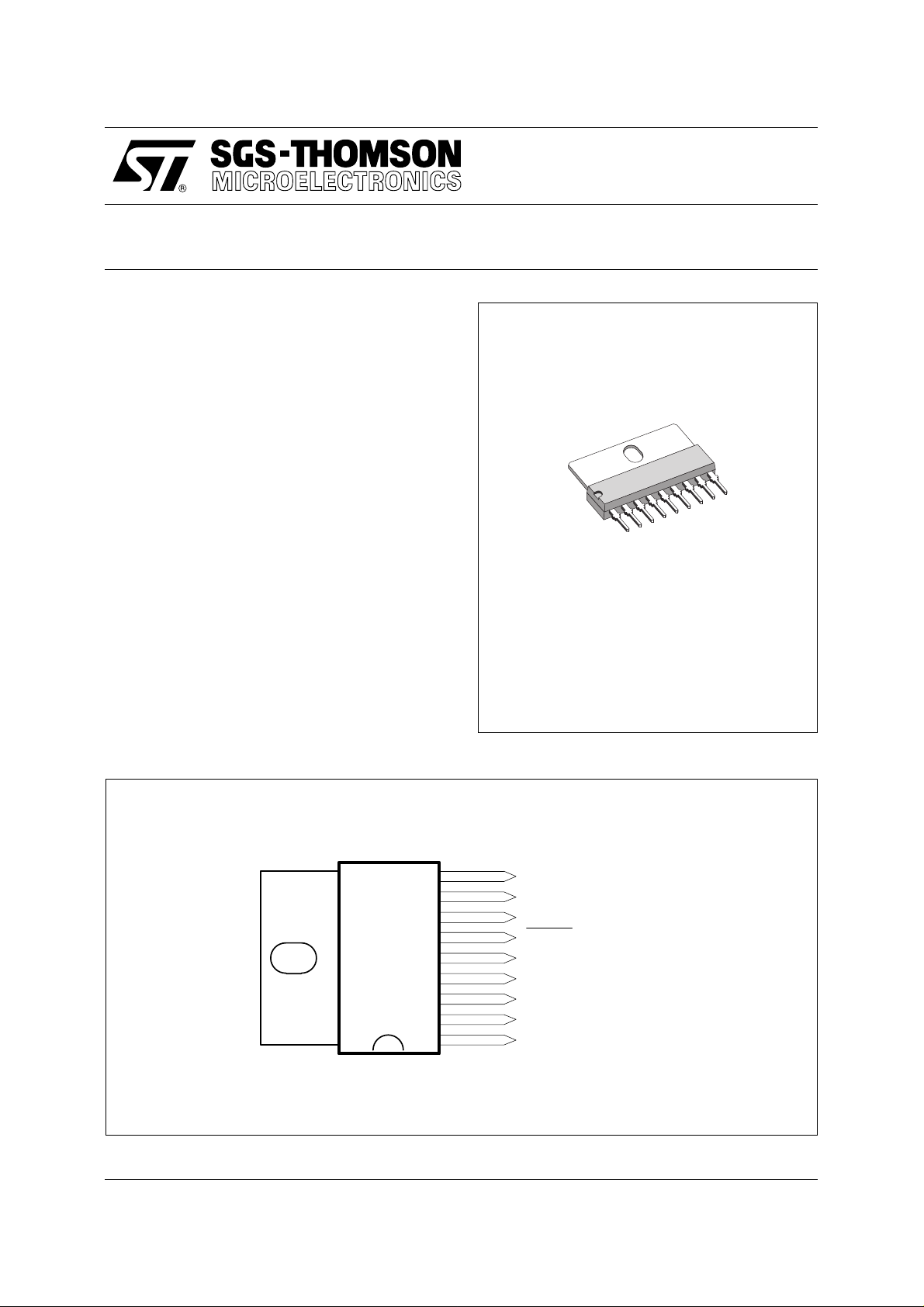
TDA8139
WITH DISABLE AND RESET
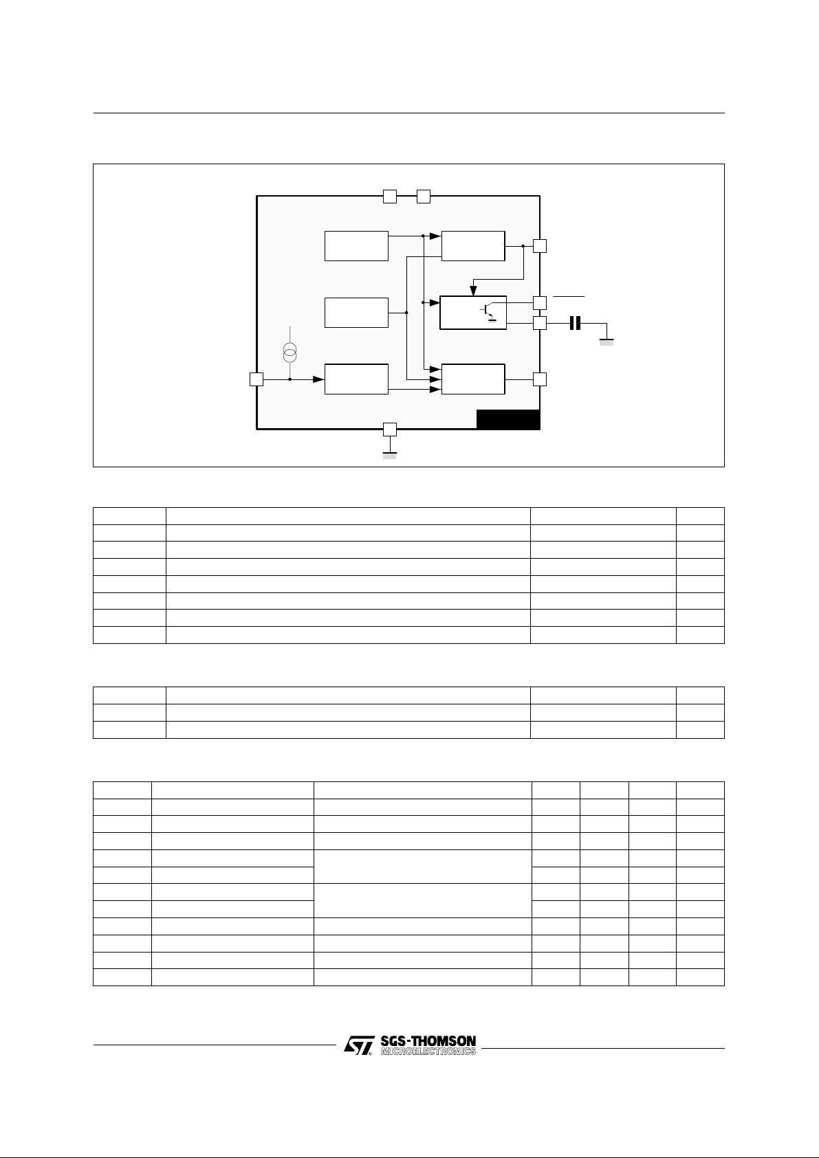
DESCRIPTION
The TDA8139 is a monolithic dual positiv e volt age
regulator designed to provide precision out put voltages of 5.1V and adjustable at currents up to
750mA.
An internal reset circuit generates a reset pulse
when the output 1 decrease below the regulated
voltage value.
Output 2 can be disabled by TTL input.
Short circuit and thermal protect ions are inclu ded.
PIN CONNECTIONS
9
8
7
6
5
4
3
2
1
SIP9
(Plastic Package)
ORDER CODE : TDA8139
OUTPUT 1
OUTPUT 2
PROGRAM
RESET
GROUND
DISABLE
DELAY CAPACITOR
INPUT 2
INPUT 1
September 1993
8139-01.EPS
1/5
TDA8139
BLOCK DIAGRAM
IN 2IN 1
12
REFERENCE
PROTECTION
4
DISABLE
5
OUT 1
RESET
OUT 2
TDA8139
OUT 1
9
6
RESET
3
DELAY
CAPACITOR
8
OUT 2DISABLE
ABSOLUTE MAXIMUM RATINGS
Symbol Parameter Value Unit
V
V
V
I
O1, 2
T
T
IN
DIS
RST
P
STG
DC Input Voltage Pin 1, 2 20 V
Disable Input Voltage Pin 4 20 V
Output Voltage at Pin 6 20 V
Output Currents Internally Limited
Power Dissipation Internally Limited
t
Storage Temperature – 65 to + 150 °C
unction Temperature 0 to + 150 °C
J
8139-02.EPS
8139-01.TBL
THERMAL DATA
Symbol Parameter Value Unit
R
TH(j-c)
T
Thermal Resistance Junction-case Max. 8 °C/W
Recommended Junction Temperature Max. 130 °C
J
ELECTRICAL CHARACT E RIS TICS ( VIN = 7V ; Tj = 25oC unless otherwise specified)
Symbol Parameter Test Conditions Min. Typ. Max. Unit
Output Voltage IO1 = 10mA 5 5.1 5.2 V
O1
Output Voltage IO2 = 10mA 2.8 16 V
O2
Dropout Voltage I
Line Regulation 1 7V < V
O1
Line Regulation 2 100 mV
O2
Load Regulation 1 5mA < I
O1
Load Regulation 2 200 mV
O2
Quiescent Current IO1 = 10mA, Output 2 Disabled 2 mA
I
Q
= 750mA 1.4 V
O1, 2
IN1
VO2 : 10V, I
O1, 2
< 14V, 12V < V
= 200mA
O1, 2
< 0.6A, @ VO2 = 10 V 100 mV
< 18V, @
IN2
Reset Threshold Voltage (K = VO1) K – 0.4 K – .25 K – 0.1 V
Reset Threshold Hysteresis (see circuit description) 20 50 75 mV
RTH
Reset Pulse Delay at Pin 6 Ce = 100nF (see circuit description) 25 ms
RD
50 mV
2/5
V
V
V
V
V
V
V
V
O1RST
V
IO1, 2
t
8139-02.TBL
8139-03.TBL
 Loading...