

5.1V +12V REGULATOR WITH DISABLE AND RESET
.
OUTPUT CURRENTS UP TO 1A
.
FIXED PRECISION OUTPUT 1 VOLTAGE
5.1V +/- 2%
.
FIXED PRECISION OUTPUT 2 VOLTAGE
12V +/- 2%
.
OUTPUT 1 WI T H RE S ET FAC ILITY
.
OUTPUT 2 WITH DISABLE BY TTL INPUT
.
SHORT CIRCUIT PROTECTION AT BOTH
OUTPUTS
.
THERMAL PROTE CTION
.
LOW DROP OUTPUT VOLTAGE
.
AVAILABLE ALSO IN HEPTAWATT PACKAGE
IN TWO VERSIONS : TDA8138A (DISABLE
ONLY), TDA8138B (RESET ONLY)
DESCRIPTION
The TDA8138 is a monolithic dual positive v oltage
regulator designed to provide fixed precision output
voltages of 5.1V and 12V at currents up to 1A.
An internal reset circuit generates a reset pulse
when the output 1 decrease below the regulated
voltage value (for TDA8138 and TDA8138B).
Output 2 can be disabled by TTL input (for
TDA8138 and TDA8138A).
Short circuit and thermal protections are included
in all the versions.
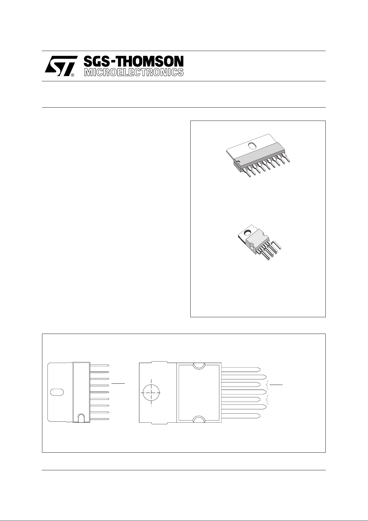
TDA8138
SIP9
(Plastic Package)
ORDER CODE : TDA8138
HEPTAWAT
(Plastic Package)
ORDER CODE : TDA8138A / TDA8138B
PIN CONNECTIONS
SIP9
9
8
7
6
5
4
3
2
1
Tab. connected to Pin 5
May 1993
OUTPUT 1
OUTPUT 2
N.C.
RESET
GROUND
DISABLE
DEL. CAP.
INPUT 2
INPUT 1
HEPTAWATT
7
6
5
4
3
2
1
Tab. connected to Pin 4
OUTPUT1
OUTPUT2
N.C. FOR TDA8138A
RESET FOR TDA8138B
GROUND
DISABLEFOR TDA8138A
DEL. CAPA FOR TDA8138B
INPUT 2
INPUT 1
8138-01A.EPS - 8138-01B.EPS
1/6
TDA8138
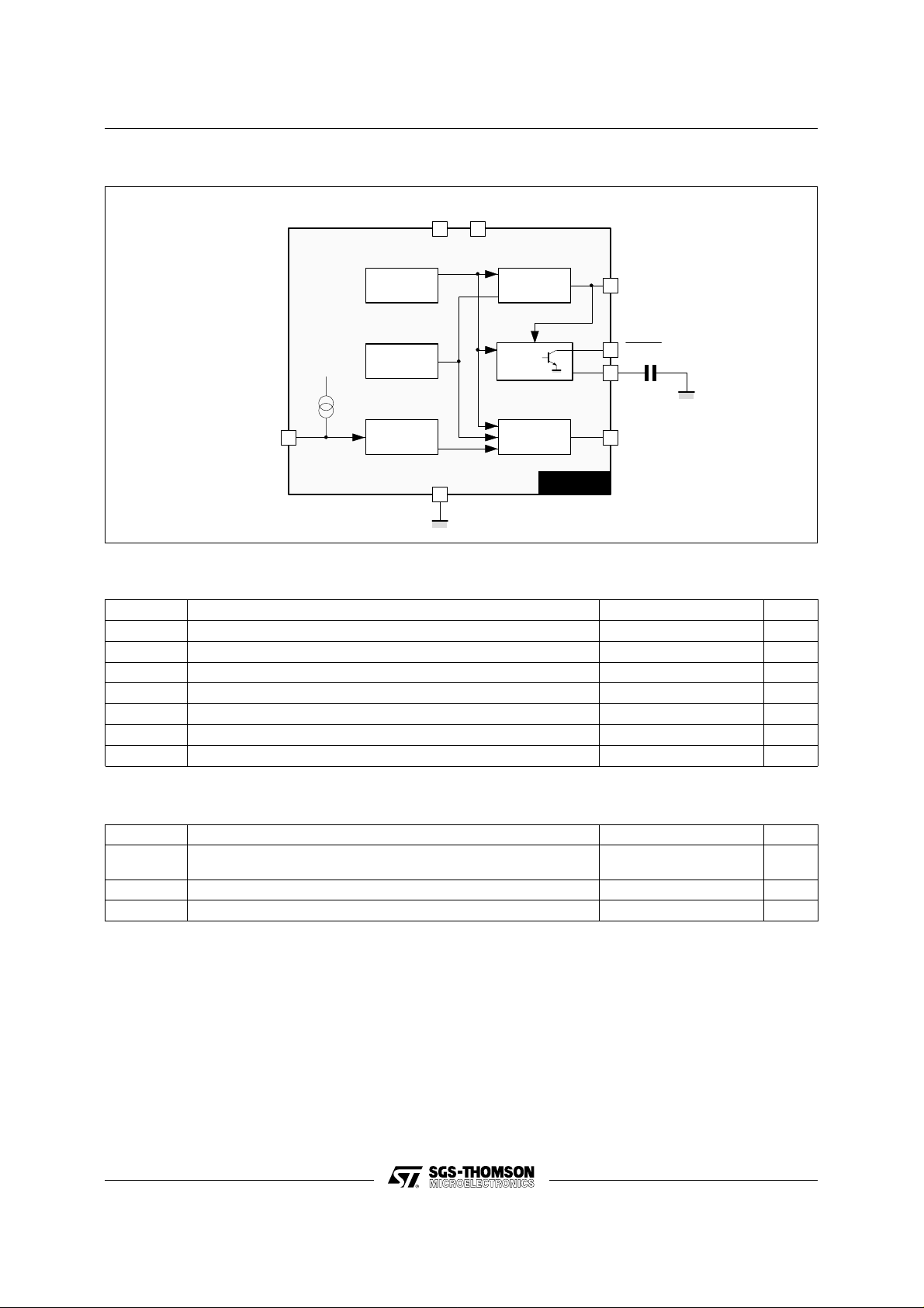
BLOCK DIAGRAM (SIP9 package)
IN 2IN 1
12
DISABLE
REFERENCE
PROTECTION
4
DISABL E
5
OUT 1
RESET
OUT 2
TDA8138
OUT 1
9
6
RESET
3
DELAY
CAPACITOR
8
OUT 2
ABSOLUTE MAXIMUM RATING S
Symbol Parameter Value Unit
V
V
V
I
O1, 2
T
IN
DIS
RST
P
stg
T
DC Input Voltage Pin 1 20 V
Disable Input Voltage Pin 3 (Heptawatt) or Pin 4 (SIP9) 20 V
Output Voltage at Pin 6 (SIP9) or Pin 5 (Heptawatt) 20 V
Output Currents Internally Limited
Power Dissipation Internally Limited
t
Storage Temperature -65 to +150
Junction Temperature 0 to +150
j
8138-02.EPS
o
C
o
C
8138-01.TBL
THERMAL D ATA
Symbol Parameter Value Unit
2/6
R
R
th (j-c)
th (j-a)
T
j
Maximum Thermal Resistance Junction-case for SIP9
Maximum Thermal Resistance Junction-case for Heptawatt
Maximum Thermal Resistance Junction-ambient for SIP9 60
Maximum Recommended Junction Temperature 130
8
3
o
C/W
o
C/W
o
C/W
o
C
8138-02.TBL

TDA8138
ELECTRICAL CHRACTERISTICS (V
= 7V, V
IN1
= 14V, Tj = 25oC, unless otherwise specified)
IN2
Symbol Parameter Test Conditions Min. Typ. Max. Unit
V
V
V
V
V
IO1,2
V
O1,2LI
V
O1,2LO
V
O1RST
V
t
V
I
K
I
O1,2SC
V
DISH
V
I
T
Note : Safe permanent short-circuit is only guaranteed for input volta g es up to 16V.
Output Voltage IO1 = 10mA 5 5.1 5.2 V
O1
Output Voltage IO2 = 10mA 11.76 12 12.24 V
O2
Output Voltage 7V < V
O1
Output Voltage 11.5 12.5 V
O2
Dropout Voltage I
14 < V
5mA < I
O1,2
I
O1,2
Line Regulation 7V < V
14 < V
I
O1,2
< 14V
IN1
< 18V
IN2
< 750mA
O1,2
= 750mA
= 1A
< 14V
IN1
< 18V
IN2
= 200mA
4.9 5.3 V
Load Regulation 5mA < IO1 < 0.6A
5mA < I
Quiescent Current IO1 = 10mA
I
Q
Output 2 Disabled
Reset Thrseshold Voltage K = V
Reset Thrseshold Hysteresis See circuit description 20 50 75 mV
RTH
Reset Pulse Delay Ce = 100nF
RD
Saturation Voltage in Reset Condition I5 = 5mA 0.4 V
RL
Leakage Current in Normal Condition
RH
(at Pin 6 for SIP9 or Pin 5 for Heptawatt)
Output Voltage Thermal Drift Tj = 0 to 125oC
O1,2
Short Circuit Output Current V
See circuit description
V5 = 10V 10 µA
K
O
IN1
V
IN1,2
< 0.6A
O2
O1
⋅ 10
O
∆T ⋅ V
O
IN2
6
= 14V
∆V
=
= 7V, V
= 16V (see Note)
K - 0.4 K -
0.25
25 ms
100 ppm/oC
Disable Voltage High (out 2 active) 2 V
Disable Voltage Low (out 2 disabled) 0.8 V
DISL
Disable Bias Current 0V < V
DIS
Junction Temperature for Thermal Shut
jsd
Down
< 7V -100 2 µA
DIS
145
1.4
2
50
120
100
250
2mA
K - 0.1 V
1.6
1
V
V
mV
mV
mV
mV
A
A
o
C
8138-03.TBL
CIRCUIT DESCRIPTION
The TDA8138 is a dual voltage regulator with Reset
and Disable (TD8138A : Disable only, TDA8138B :
Reset only).
The two regulation parts are supplied from one
voltage reference circuit trimmed by zener zap
during EWS test.
Since the supply voltage of this last is connected at
Pin 1 (V
), the regulator 2 will not work if Pin 1 is
IN1
not supplied.
The outputs stage have been realized in darlington
configuration with a drop typical 1.2V.
The disable circuit, switch-off the output 2 if a
voltage lower than 0.8V is applied at Pin 3
(Heptawatt) or Pin 4 (SIP9)
The Reset circuit checks the voltage at the out-
put 1. If this one goes below V
- 0.25V (4.85V
OUT
typ.), the com parator "a" (see Figure 1) dis charges
rapidly the capacitor C
and the reset output goes
e
at once Low. When the voltage at the out1 rises
above V
- 0.2V (4.9V typ.), the voltage V
OUT
Ce
increases linearly to 2.5V corresponding to a delay
td following the law : t
=
1
10
(see Figure 2),
µA
C
⋅ 2.5V
e
then the reset output goes high again. To avoid
gliches in the reset output, the sec ond c omparat or
"b" has a large hysteresis (1.9V).
3/6
TDA8138
Figure 1
OUT 1
10µA
RESET
REF
2.5V
9
a
+
50
-
b
+
6
3
Figure 2
5.1V
4.9V
4.85V
RESET
REG
C
e
T
D
2.5V 0.6V
T
D
Vout LOW
∆
8138-03.EPS
8138-04.EPS
TYPICAL APPLICATION (SIP9 package)
V
IN1
V
IN2
C1 C2 C3 C4
4/6
1
2
RESET
6
TDA8138
5
C1 to C4 = 10 µF
Ce
3
4
DISABLE
0.1
F
µ
9
8
V
O1
V
O2
8138-05.EPS

PACKAGE MECHANICAL DATA
9 PINS - PLASTIC HEPTAW ATT
TDA8138
Dimensions
L
L1
A
C
D1
L5
H3
Dia.
L7
L6
D
L2
L3
F1
Millimeters Inches
Min. Typ. Max. Min. Typ. Max.
H2
E
MM1
G
F
G1
G2
A 4.8 0.189
C 1.37 0.054
D 2.4 2.8 0.094 0.110
D1 1.2 1.35 0.047 0.053
E 0.35 0.55 0.014 0.022
F 0.6 08 0.024 0.031
F1 0.9 0.035
G 2.41 2.54 2.67 0.095 0.100 0.105
G1 4.91 5.08 5.21 0.193 0.200 0.205
G2 7.49 7.62 7.8 0.295 0.300 0.307
H2 10.4 0.409
H3 10.05 10.4 0.396 0.409
L 16.97 0.668
L1 14.92 0.587
L2 21.54 0.848
L3 22.62 0.891
L5 2.6 3 0.102 0.118
L6 15.1 15.8 0.594 0.622
L7 6 6.6 0.236 0.260
M 2.8 0.110
M1 5.08 0.200
Dia. 3.65 3.85 0.144 0.152
PM-HEPTV.EPS
HEPTV.TBL
5/6

TDA8138
PACKAGE MECHANICAL DATA
9 PINS - PLASTIC SIP
C
c2
A
c1
Dimensions
L2
D
L1
19
a1
L
e3
N
M
b1
b3
e
B
L3
d1
Millimeters Inches
Min. Typ. Max. Min. Typ. Max.
A 7.1 0.280
a1 2.7 3 0.106 0.118
B 24.8 0.976
b1 0.5 0.020
b3 0.85 1.6 0.033 0.063
C 3.3 0.130
c1 0.43 0.017
c2 1.32 0.052
D 21.2 0.835
d1 14.5 0.571
e 2.54 0.100
e3 20.32 0.800
L 3.1 0.122
L1 3 0.118
L2 17.6 0.693
L3 0.25 0.010
M 3.2 0.126
Information furnished i s believed to be accurate and rel iabl e. However, S GS-THOMSON Microel ectroni cs assumes no responsibil ity
for the consequences of use of such information nor for any infringement of patents or other rights of third parties which may result
from its use. No licence is granted by implication or otherwise under any patent or patent rights of SGS-THOMSON Microelectronics.
Specifications mentioned in this publication are subject to change without notice. This publication supersedes and replaces all
information previously supplied. SGS-THOMSON Microelectronics products are not authorized for use as critical components in life
support devices or systems without express written approval of SGS-THOMSON Microelectronics.
PM-SIP9.EPS
SIP9.TBL
6/6
© 1994 SGS-THOMSON Microelec tronics - All Rights Reserved
2
Purchase of I
2
C Patent. Rights to use these components in a I2C system, is granted provided that the system conforms to
I
Australia - Brazil - China - France - Germany - Hong Kong - Italy - Japan - Korea - Malaysia - Malta - Morocco
The Netherlands - Singapore - Spain - Sweden - Switzerland - Taiwan - Thailand - United Kingdom - U.S.A.
C Components of SGS-THOMSON Microelectronics, conveys a license under the Philips
2
C Standard Specifications as defined by Philips.
the I
SGS-THOMSON Microelectronics GROUP OF COMPANIES
 Loading...