

FM/AM DIGITAL IF SAMPLING PROCESSOR
■
FM/AM IF SAMPLING DSP
■
ON-CHIP ANALOGUE TO DIGITAL
CONVERTER FOR 10.7MHz IF SIGNAL
CONVERSION
■
SOFTWARE BASED CHANNEL EQUALIZATION
■
FM ADJACENT CHANNEL SUPPRESSION
■
RECEPTION ENHANCEMENT IN MULTIPATH
CONDITION
■
STEREO DECODER AND WEAK SIGNAL
PROCESSING
■
2 CHANNELS SERIAL AUDIO INTERFACE
(SAI) WITH SAMPLE RATE CONVERTER
■
I2C AND BUFFER-SPI CONTROL INTERFACES
■
RDS FILTER, DEMODULATOR & DECODER
■
INTER PROCESSOR TRA NS PO RT
INTERFACE FOR ANTENNA AND TUNER
DIVERSITY
■
FRONT-END AGC FEEDBACK
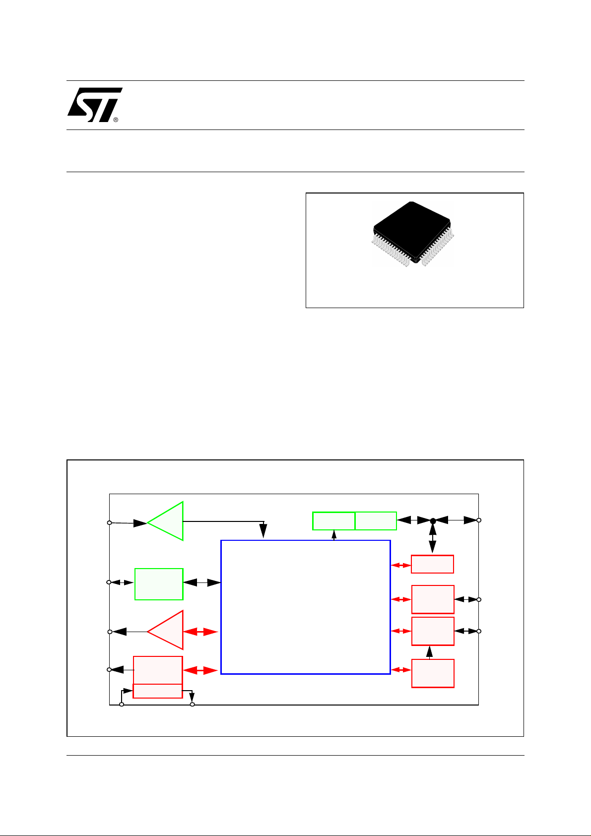
TDA7580
PRODUCT PREVIEW
TQFP64
ORDERING NUMBER: TDA7580
DESCRIPTION
The TDA7580 is an integrated circuit implementing
an advanced mixed analogue and digital solution to
perform the signal processing of a AM/FM channel.
The HW&SW architecture has been devised so to
have a digital equalization of the FM/AM channel;
hence a real rejection of adjacent channels and any
other signals interfering with the listening of the desired station. In severe Multipl e Paths conditi ons, the
reception is improved to get the audi o with hi gh quality.
BLOCK DIAGRAM
Oscillator
HS3I
CGU
A/D
DAC
RDS
I2C/SPI
IF Digital
Signal Processor
I2C/SPI
SAI1
SAI0
SRC
July 2002
This is preliminary information on a new product now in development. Details are subject to change without notice.
1/31

TDA7580
DESCRIPTION
(continued)
The algorithm is self-adaptive, thus it requires no “on-the-field” adjustments after the parameters optimization.
The chip embeds a
Band Pass Sigma Delta Analogue to Digital Converter
for 10.7MHz IF conversion from a
“tuner device” (it is highly recommended the TDA7515).
The internal 24bit-DSP allows some flexibility in the algorithm implementation, thus giving some freedom for
customer required features. The total processing power offers a significant headroom for customer’s software
requirement, even when the channel equalization and the decoding software is running. The Program and Data
Memory space can be loaded from an external non volatile memory via I
2
C or SPI.
The oscillator module works with an external 74.1MHz quartz crystal. It has very low Electro Magnetic Interference, as it introduces very low distortion, and in any case any harmonics fall outside the Radio bandwidth.
The companion tuner device receives the reference clock through a differential ended interface, which works
off the Oscillator module by properly dividing down the master clock frequency. That allows the overall system
saving an additional crystal for the tuner.
After the IF convers ion, the digitiz ed baseband signal pass es through th e B ase Band pr oces sing section, either
FM or AM, depending on the listener selection. The FM Base Band processing comprises of Stereo Decoder,
Spike Detection and Noise Blanking. The AM Noise Blanking is fully software implemented.
The internal RDS filter, de modulator and dec oder featur es com plete functi ons to hav e the output data avail able
through either I
2
C or SPI interface. No DSP support is needed but at start-up, so that RDS can work in background and in parallel with other DSP pr ocess ing. Thi s mode (RDS-onl y) all ows cur rent c onsumption savi ng for
low power application modes.
2
An I
C/SPI interface is available for any control and communication with the main micro, as well as RDS data
interface. The DSP SPI block embeds a 10 words FIFO for both transmit and receive channels, to lighten the
DSP task and frequently respond to the interrupt from the control interface.
Serial Audio Interface (SAI) is the ideal solution for the audio data transfer, both transmit and receive: either
master or slave. The flexibility of this module gives a wide choice of different protocols, including I
2
S. Two fully
independent bidirectional data channels, with separate clocks allows the use of TDA7580 as general purpose
digital audio processor.
A fully Asynchronous Sample Rate Converter (ASR C) is available as a peripheral prior to sending audio data
out via the SAI, so that internal audio sampling rate (~36kHz and FM/AM mode) can be adapted by upconversion to any external rate.
An Inter Processor Transport Interface (HS
modular system which implements
Dual Tuner Diversity
3
I, High Speed Synchronous Serial Interface) is also available for a
, thus enhancing the overall system performance. It is
about a Synchronous Serial Interfac e which exchan ges data up to the MPX rate. It has been designed to reduce
the Electro Magnetic Interference toward the sensitive analogue signal from the Tuner.
General Purpose I/O registers are connected to and controlled by the DSP, by means of memory map.
A Debug and Test Interface is available for on-chip software debug as well as for internal registers read/write
operation.
2/31
TDA7580
ABSOLUTE MAXIMUM RATINGS
Symbol Parameter Value Unit
VDD
VDD3
Power supplies
Analog Input or Output Voltage belonging to 3.3V IO ring (V
V
DDOSC
Digital Input or Output Voltage, 5V tolerant
All remaining Digital Input or Output Voltage Nom. 1.8V
T
T
stg
Warning: Operat ion at or be yo nd thes e limi ts ma y resu lt in p erma ne nt dam age t o the d evic e. No rma l oper ation is not guara nt eed at these
Note: 1. V
2. During N orm al Mode operation VDD3 is al ways available as specified
3. During Fail-safe Mode operation VDD3 may be not available.
Operating Junction Temperature Range -40 to 125 °C
j
Storage Temperature -55 to 150 °C
extremes.
refers to all of the nom i nal 3.3V power supplies (V
DD3
, V
MTR
).
(V
DD
(1)
Nom. 1.8V
Nom. 3.3V
DDSD
-0.5 to 2.5
-0.5 to 4.0
,
-0.5 to 4.0 V
V
V
)
DDH
, V
OSC
Normal
Fail-safe
Nom. 3.3V
, V
DDSD
(2)
(3)
). V
refers to all of the nominal 1.8V power supplies
DD
-0.5 to 6.50
-0.5 to 3.80
-0.5 to (VDD+0.5)
-0.5 to (VDD3+0.5)
V
V
V
THERMAL DATA
Symbol Parameter Value Unit
R
th j-amb
Thermal resistance junction to ambient 68 °C/W
3/31
TDA7580
PIN CONNECTION
VHI
VCM
VLO
INP
INN
VCMOP
GNDSD
GNDOSC
XTI
XTO
VDDOSC
VDDMTR
CKREFP
CKREFN
AGCKEY
GNDMTR
(Top view)
VDDSD63VDDH62GNDH61VDDISO60GND59VDD58DBOUT157DBRQ156DBIN155DBCK154VDDH53GNDH52DBOUT051DBRQ050DBIN049DBCK0
64
1
2
DEBUG1
DEBUG0
3
4
5
IFADC
6
7
8
9
10
OSC.Tuner
11
12
13
14
15
16
17
C/SPI
2
DSP/RDS
I
19
18
20
21
22
HS3I
23
24
25
26
27
28
RDS
29
30
SAI
31
48
47
46
45
44
43
42
41
40
39
38
37
36
35
34
33
32
GND
VDD
TST3_LRCKR
TST2_SCKR
LRCK_LRCKT
SCLK_SCKT
SDO0
VDDH
GNDH
TST1_SDI1
TST4_SDI0
GPIO_SDO1
TESTN
GND
VDD
RESETN
4/31
VDD
SCL_SCK
GND
IQSYNC
IQCH1
IQCH2
IQCH3
VDDH
GNDH
RDS_INT
RDS_CS
MISO
SDA_MOSI
PROTSEL_SS
IFADC Modulator Power Supply pins pair
Oscillator Power Supply pins pair
Tuner Clock Out and AGC Keying DAC Power Supply pins pair
Core Logic 1.8V Power Supply pins pair
I/O Ring 3.3V Power Supply pins pair
INT
ADDR_SD
PIN DESCRIPTION
N° Name Type Description Notes
TDA7580
After
Reset
1 VHI A Internally generated IFADC Opamps
2.65V (@VDD=3.3V) Reference Voltage
Pin for external filtering
2 VCM A Internally generated Common Mode
1.65V (@VDD=3.3V) Reference Voltage
Pin for external filtering
3 VLO A Internally generated IFADC Opamps
0.65V (@VDD=3.3V) Reference Voltage
Pin for external filtering
4 INP A Positive IF signal input from Tuner 2.0Vpp @VDD=3.3V
5 INN A Negative IF signal input from Tuner 2.0Vpp @VDD=3.3V
6 VCMOP A Internally generated Modulator Opamps
Common Mode 2.65V (@VDD=3.3V)
Reference Voltage Pin for external
filtering
7 GNDSD G IFADC Modulator Analogue Ground Clean Ground, to be
8 GNDOSC G Oscillator Ground Clean Ground, to be
9 XTI I High impedance oscillator input (quartz
connection) or clock input when in
Antenna Diversity slave mode
It needs external 22µF
and 220nF ceramic
capacitors
It needs external 22µF
and 220nF ceramic
capacitors
It needs external 22µF
and 220nF ceramic
capacitors
It needs external 22µF
and 220nF ceramic
capacitors
star-connected to
voltage regulator ground
star-connected to
voltage regulator ground
Maximum voltage swing
is VDD
10 XTO O Low impedance oscillator output (quartz
11 VDDOSC P Oscillator Power Supply 3.3V
12 VDDMTR P Tuner reference clock and AGCKeying
13 CKREFP B Tuner reference clock positive output. FM 100kHz
14 CKREFN B Tuner reference clock negative output. FM 100kHz
15 AGCKEY A DAC output for Tuner AGCKeying 1.5kohm ±30% output
16 GNDMTR G Tuner reference clock and AGC keying
connection)
DAC Power Supply
DAC Ground
1.8V
18kHz
AM
EU
With internal pull_up, on
at reset
AM
18kHz
EU
With internal pull_up, on
at reset
impedance. 1Vpp ±1%
output dynamic range
Output
Output
5/31
TDA7580
PIN DESCRIPTION
(continued)
N° Name Type Description Notes
17 PROTSEL_SS B DSP0 GPIO for Control Serial Interface
2
(Low: SPI or High: I
C) selection at
device Bootstrap.
In SPI protocol mode, after Boot
DSP0 GPIO0
5V tolerant
With internal pull_up, on
at reset
procedure, SPI Slave Select, otherwise
DSP0 GPIO0
18 SDA_MOSI B Control Serial Interface and RDS IO:
- SPI mode: slave data in or master data
out for main SPI and RDS SPI data in
2
C mode: data for main I2C or RDS I2C
- I
19 MISO B SPI slave data out or master data in for
main SPI and RDS SPI data out
5V tolerant
With internal pull_up, on
at reset
DSP0 GPIO1
5V tolerant
With internal pull_up, on
at reset
20 SCL_SCK B Bit clock for Control Serial Interface and
RDS
5V tolerant
With internal pull_up, on
at reset
21 GND G Digital Core Power Ground
22 VDD P Digital Core Power Supply 1.8V
After
Reset
Input
Input
Input
Input
23 IQSYNC B High Speed Synchronous Serial
3
Interface (HS
I) clock if HS3I master
mode, else DSP1 GPIO or DSP1 Debug
Port Clock (DBOUT1)
24 IQCH1 B High Speed Synchronous Serial
3
Interface (HS
I) Channel 1 Data if HS3I
master mode, else DSP1 GPIO or DSP1
Debug Port Request (DBRQ1)
25 IQCH2 B High Speed Synchronous Serial
3
Interface (HS
I) Channel 2 Data if HS3I
master mode, else DSP1 GPIO or DSP1
Debug Port Data In (DBIN1)
26 IQCH3 B High Speed Synchronous Serial
3
Interface (HS
I) Channel 3 Data if HS3I
master mode, else DSP1 GPIO or DSP1
Debug Port Data Out (DBCK1)
27 VDDH P
3.3V IO Ring Power Supply (HS
SPI, RDS, INT)
28 GNDH G
3.3V IO Ring Power Ground (HS
SPI, RDS, INT)
29 RDS_INT B RDS interrupt to external main
microprocessor in case of traffic
information
3
I, I2C/
3
I, I2C/
DSP1 GPIO0
5V tolerant
With internal pull_up, on
at reset
DSP1 GPIO1
5V tolerant
With internal pull_up, on
at reset
DSP1 GPIO2
5V tolerant
With internal pull_down,
on at reset
DSP1 GPIO3
5V tolerant
With internal pull_down,
on at reset
DSP1 GPIO4
5V tolerant
With internal pull_up, on
at reset
Input
Input
Input
Input
Input
6/31
TDA7580
PIN DESCRIPTION
N° Name Type Description Notes
30 RDS_CS B RDS chip select. When RESETN rising,
31 INT I DSP0 External Interrupt 5V tolerantWith internal
32 ADDR_SD B IFS chip master (Low) or slave (High)
33 RESETN I Chip Hardware reset, active Low 5V tolerant
34 VDD P Digital Power Supply 1.8V
35 GND G Digital Power Ground
36 TESTN I Test Enable pin, active Low With internal pull_up
37 GPIO_SDO1 B DSP0 GPIO for Boot selection or Audio
(continued)
If RDS_CS 0, the RDS’s SPI is selected;
else RDS’s I
mode selection, latched in upon
RESETN release. It selects the LSB of
2
the I
Station Detector output
SAI0 output.
2
C
C addresses.
DSP1 GPIO5
5V tolerant
With internal pull_up, on
at reset
pull_up, on at reset
DSP0 GPIO2
5V tolerantWith internal
pull_down, on at reset
With internal pull_up
5V tolerant
DSP0 GPIO3
With internal pull_up, on
at reset
After
Reset
Input
Input
Input
38 TST4_SDI0 B Audio SAI0 Data input or test selection
pin in Test Mode
39 TST1_SDI1 B DSP0 GPIO for Boot selection or Audio
SAI1 input. Test selection pin in Test
Mode.
40 GNDH G 3.3V IO Ring Power Ground (Audio SAI,
ResetN, Test Pins)
41 VDDH P 3.3V IO Ring Power Supply (Audio SAI,
ResetN, Test Pins)
42 SDO0 B Radio or Audio SAI0 data output 5V tolerant
43 SCLK_SCKT B SAI0 Receive and Transmit bit clock
(master or slave with ASRC); SAI1
Transmit bit clock
44 LRCK_LRCKT B SAI0 Receive and Transmit LeftRight
clock (master or slave with ASRC); SAI1
Transmit LeftRight clock
5V tolerant
DSP0 GPIO5With
internal pull_up, on at
reset
5V tolerant
DSP0 GPIO4With
internal pull_up, on at
reset
With internal pull_up, on
at reset
5V tolerant
With internal pull_up, on
at reset
5V tolerant
With internal pull_up, on
at reset
Input
Input
Output
Input
Input
7/31
TDA7580
PIN DESCRIPTION
(continued)
N° Name Type Description Notes
45 TST2_SCKR B SAI0 Transmit bit clock; SAI1 Receive
and Transmit bit clock. Or Test selection
pin in Test Mode
5V tolerant
DSP0 GPIO6
With internal pull_up, on
at reset
46 TST3_LRCKR B SAI0 Transmit LeftRight clock; SAI1
Receive and Transmit bit clock. Or Test
selection pin in Test Mode
DSP0 GPIO7
5V tolerant
With internal pull_up, on
at reset
47 VDD P Digital Core Power Supply 1.8V
48 GND G Digital Core Power Ground
49 DBCK0 B Debug Port Clock of DSP0 (DBCK0) DSP0 GPIO9
5V tolerant
With internal pull_down,
on at reset
50 DBIN0 B Debug Port Data Input of DSP0 (DBIN0) DSP0 GPIO11
5V tolerant
With internal pull_down,
on at reset
51 DBRQ0 B Debug Port Request of DSP0 (DBRQ0) DSP0 GPIO
5V tolerant
With internal pull_up, on
at reset
After
Reset
Input
Input
Input
Input
Input
52 DBOUT0 B Debug Port Data Output of DSP0
(DBOUT0)
53 GNDH G 3.3V IO Ring Power Ground (Debug
Interface, GPIO)
54 VDDH P 3.3V IO Ring Power Supply (Debug
Interface, GPIO)
55 DBCK1 B
DSP1 Debug Port Clock (DBCK1) if HS
master mode, else High Speed
3
Synchronous Serial Interface (HS
I)
Channel3 Data
56 DBIN1 B DSP1 GPIO or DSP1 Debug Port Data
3
In (DBIN1) if HS
I master mode, else
High Speed Synchronous Serial
Interface (HS
3
I) Channel2 Data i
57 DBRQ1 B DSP1 GPIO or DSP1 Debug Port
3
Request (DBRQ1) if HS
I master mode,
else High Speed Synchronous Serial
Interface (HS
3
I) Channel1 Data
DSP0 GPIO10
5V tolerant
With internal pull_up, on
at reset
3
DSP1 GPIO9
I
5V tolerant
With internal pull_down,
on at reset
DSP1 GPIO11
5V tolerant
With internal pull_down,
on at reset
5V tolerant
With internal pull_up, on
at reset
Input
Input
Input
Input
8/31
TDA7580
PIN DESCRIPTION
N° Name Type Description Notes
58 DBOUT1 B DSP1 GPIO or DSP1 Debug Port Data
VDD
59
GND
60
61 VDDISO P 3.3V N-isolation biasing supply Clean 3.3V supply to be
GNDH
62
VDDH
63
VDDSD
64
(continued)
3
Out (DBOUT1) if HS
else High Speed Synchronous Serial
Interface (HS
P Digital Core Power Supply 1.8V
G Digital Core Power Ground
G 3.3V IO Ring Power Ground (Modulator
digital section)
P 3.3V IO Ring Power Supply (Modulator
digital section)
P 3.3V IFADC Modulator Analogue Power
Supply
3
I master mode,
I) clock
DSP1 GPIO10
5V tolerant
With internal pull_up, on
at reset
star-connected to
voltage regulator
Clean Power Supply, to
be star-connected to
3.3V voltage regulator
After
Reset
Input
I/O TYPE
P: Power Supply from Voltage regulator
G: Power Ground from Voltage regulator
A: Analogue I/O
I: Digital Input
O: Digital Output
B: Bidirectional I/O
I/O DEFINITION AND STATUS
Z: high impedance (input)
O: logic low output
X: undefined output
1: logic high output
Output
PP
: Push-Pull/ OD: Open-Drain
9/31
TDA7580
RECOMMENDED DC OPERATING CONDITIONS
Symbol Parameter Comment Min. Typ. Max. Unit
V
V
V
V
DDSD
V
Note: 1. V
1.8V Power Supply Voltage Core Power Supply 1.7 1.80 1.9 V
DD
3.3V Power Supply Voltage (1) IO Rings Power Supply (with G
DDH
3.3V Power Supply Voltage (1) Oscillator Power Supply (GND
OSC
3.3V Power Supply Voltage (1) IF ADC Power Supply (with G
1.8V Power Supply Voltage DAC-Keying and Tuner clock
MTR
Power Supply (with GND
, V
, V
DDH
OSC
are also indi cated in this document as V
DDSD
. All othe rs as VDD.
DD3
) 3.15 3.30 3.45 V
NDH
) 3.15 3.30 3.45 V
OSC
) 3.15 3.30 3.45 V
NDSD
1.7 1.80 1.9 V
)
MTR
GENERAL INTERFACE ELECTRICAL CHARACTERISTICS
Symbol Parameter Test Condition Min. Typ. Max. Unit
l
I
ipdh
l
Low Level Input Current
ilh
I/Os@V
High Level Input Current
ihh
I/Os@V
Low Level Input Current
l
il
I/Os@V
High Level Input Current
l
ih
I/Os@V
DD3
DD3
DD
DD
Pull-down current I/Os @ V
(absolute value)
(absolute value)
(absolute value)
(absolute value)
DD3
V
= 0V (notes 1, 2)
i
without pull-up-down device
V
= V
i
(notes 1, 2)
DD3
without pull-up-down device
V
= 0V (notes 1, 3, 4)
i
without pull-up-down device
V
= VDD (notes 1, 3, 4)
i
without pull-up device
Vi = V
DD3
(note 5)
with pull-down device
1 µA
1 µA
1 µA
1 µA
3.2 6.6 10.0 µA
I
opuh
I
opul
I
aihop
I
acm
I
I
ain
I
aik
I
Pull-up current I/Os @ V
Pull-up current I/Os @ V
DD3
DD
Analogue pin sunk/drawn current
on pin1 and pin 6
Analogue pin sunk/drawn current
on pin 2
Analogue pin sunk/drawn current
ail
on pin 3
Analogue pin sunk/drawn current
on pin 4 and pin 5
Analogue pin sunk/drawn current
on pin 15
Tri-state Output leakage Vo = 0V or V
oz
Vi = 0V(note 6)
-10.0 -6.6 -3.2 µA
with pull-up device
Vi = 0V (note 3)
-5.4 -3.6 -1.8 µA
with pull-up device
Vi = V
DD3
0.95 1.25 1.55 mA
Vi = 0V -6.25 -5.0 -3.75 mA
Vi = V
DD3
1.5 2.0 2.5 mA
Vi = 0V -2.5 -2.0 -1.5 mA
Vi = V
DD3
3.75 5.0 6.25 mA
Vi = 0V -1.55 -1.25 -0.95 mA
Vi = V
DD3
24 32 40 µA
Vi = 0V -40 -32 -24 µA
Vi = V
DD
0.8 1.2 1.6 mA
Vi = 0V (spec absolute value) 1 µA
DD3
(note 1)
1 µA
without pull up/down device
10/31

TDA7580
GENERAL INTERFACE ELECTRICAL CHARACTERISTICS
(continued)
Symbol Parameter Test Condition Min. Typ. Max. Unit
I
ozFT
5V Tolerant Tri-state Output
Vo = 0V or V
(note 1) 1 µA
dd
leakage (without pull up/down
device)
I
latchup
V
Note: 1. The leakage currents are generally very smal l , <1nA. The value given here, 1µA, is the maximum that can occur after an Electro-
I/O latch-up current V < 0V, V > V
Electrostatic Protection Leakage, 1µA 2000 V
esd
static Stress on the pin.
2. On pins:17 to 20,23 to 26,29 to 33,36 to 39,42 to 46,49 to 52,55 to 58.
3. On pins: 13 and 14.
4. Same check on the analogue pin 15 (phisically without pul l -up-down)
5. On pins:25, 26,32,49,50,55,56
6. On pins:17 to 20,23 to 24,29 to 31,33,36 to 39,42 to 46,51 , 52 ,57, 58
Vo = 5.5V 1 3 µA
dd
200 mA
LOW VOLTAGE CMOS INTERFACE DC ELECTRICAL CHARACTERISTICS
Symbol Parameter Test Condition Min. Typ. Max. Unit
V
Low Level Input Voltage 1.70V<=VDD<=1.90V
il
V
V
V
Note: 1. It is the source/sink cur rent under wo rst case condit i ons and refle ct s t he name of the I/O cell accord ing to the drive capability.
High Level Input Voltage 1.70V<=VDD<=1.90V
ih
Low level output Voltage Iol = 4mA (notes 1) 0.15 V
ol
High level output Voltage Iol = -4mA (notes 1)
oh
0.8*V
VDD-0,15
DD3
0.3*V
DD3
V
V
V
HIGH VOLTAGE CMOS INTERFAC E DC ELECTRICAL CHARACTERISTICS
Symbol Parameter Test Condition Min. Typ. Max. Unit
V
Low Level Input Voltage 3.15V<=VDD3<=3.45V
il
V
V
V
Note: 1. It is the source/sink cur rent under wo rst case condit i ons and refle ct s t he name of the I/O cell accord ing to the drive capability
High Level Input Voltage 3.15V<=VDD3<=3.45V
ih
Low level output Voltage Iol = XmA (notes 1 and 2) 0.15 V
ol
High level output Voltage Iol = -XmA (notes 1 and 2)
oh
2. X=4mA for pi ns 17 to 20,29,3 0, 32,36 to 39,42 to 46; X=8mA for pins 23 to 26,49 to 52,55 to 58.
V
2.0
DD3
-0.15
0.8
CURRENT CONSUMPTION
Symbol Parameter Test Condition Min. Typ. Max. Unit
I
I
DDH
I
I
OSCdc
Current through VDD Power
DD
Supply
Current through V
Supply
Current through VSD Power
SD
Supply
Current through V
Supply
DDH
OSC
Power
Power
VDD=1.8V,VDD3=3.3V
120 200 mA
All digital blocks working
VDD=1.8V,VDD3=3.3V
35mA
All I/Os working with 5pF load
VDD=1.8V,VDD3=3.3V 36 45 54 mA
VDD=1.8V,VDD3=3.3V
5.5 8 10.5 mA
without quartz
V
V
V
11/31

TDA7580
CURRENT CONSUMPTION
(continued)
Symbol Parameter Test Condition Min. Typ. Max. Unit
I
OSCac
I
MTR
Current through V
Supply
Current through V
OSC
MTR
Power
Power
VDD=1.8V,VDD3=3.3V
11 14 17 mA
with quartz in FM mode
VDD=1.8V,VDD3=3.3V 5 mA
Supply
Note : 7 4.1MHz internal DSP clock , at T
= 25°C. Current due to external loads not inc l uded.
amb
OSCILLATOR CHARAC TERISTICS
Symbol Parameter Test Condition Min. Typ. Max. Unit
F
OSCFM
F
OSCAM
Notes: 1. The accuracy of this figure only depends on the quartz frequency precision: high stability oscillator
Oscillator Frequency (XTI/XTO) V
Oscillator Frequency (XTI/XTO) V
@ 3.3V 74.1 MHz
OSC
@ 3.3V 74.106 MHz
OSC
QUARTZ CHARACTERISTICS
Parameter Name Parameter Value
Temperature range -55°C ÷ +125°C
Adjustment tolerance (@ 25°C ± 3°C) +/-20ppm
Frequency stability (-20°C ÷ +70°C) +/-50ppm
Aging @ 25°C 5ppm/year
Shunt (static) capacitance (Co) <6pF
Packages (holders) UM-1; HC-52U; HC-35; HC-48U; HC-49U; HC-50U; HC-51U
Mode of oscillation
Resonance resistance (ESR) <35ohm
Oscillation Frequency (without external load) ≥74108000 Hz
Oscillation Frequency (12pF parallel load) target 74.1MHz
AT-3
rd
DSP CORE
Symbol Parameter Test Condition Min. Typ. Max. Unit
F
dspMax
Maximum DSP clock frequency At 1.7V Core Power Supply and
81.5 MHz
125°C junction temperature
FM STEREO DECODER CHARACTERISTICS
Symbol Parameter Test Condition Min. Typ. Max. Unit
a_ch Channel Separation 50 dB
THD Total Harmonic Distortion 0.02 %
(S+N)/N Signal plus Noise to Noise ratio 80 dB
12/31

TDA7580
SAMPLE RATE CONVERTER
MCK = 18.525MHz, F
sin/Fsout
Symbol Parameter Test Condition Min. Typ. Max. Unit
THD+N Total Har m onic Distortion +
Noise
DR Dynamic Range
IPD Interchannel Phase Deviation 0
f
Cutoff Frequency @ -3 dB Hz
c
R
F
Pass Band Ripple from 0 to 20kHz -0.01 0.01 dB
p
R
Stopband Attenuation @24.1kHz -120 dB
s
Group Delay Fsout = 44.1 kHz 540 µs
T
g
Sampling Frequency In/Out Ratio Fsout = 44.1 kHz 0.7 1.05
ratio
= 0.820445366
20Hz to 20kHz, Full Scale, 16 bit inp.
20Hz to 20kHz, Full Scale, 20 bit inp.
1 kHz Full Scale, 16 bit inp. -95 dB
10 kHz Full Scale, 16 bit inp. -95 dB
1 kHz Full Scale, 20 bit inp. -105 dB
10 kHz Full Scale, 20 bit inp -98 dB
1 kHz -60 dB - 16 bit inp.,A-Weighted
1 kHz -60 dB - 20 bit inp.,A-Weighted
-95 dB
-98 dB
98 dB
120 dB
Degree
13/31

TDA7580
POWE R ON TIMING
Figure 1. Power on and boot sequence using I2C
VDD3
VDD
INT
RESETN
ADDR_SD
IFS SLAVE=1
IFS MA STER=0
PROTSEL_SS
RDS_CS
GPIO_SDO1
I2C/SPI SLAVE=1
TST1_SDI1
I
2
C/SP
I MASTER=0
SDA_MOSI
t
int
t
reson
t
rhd
t
rsu
Figure 2. Power on and boot sequence using SPI
VDD3
VDD
INT
RESETN
Boot
RDS init
t
seq
SW download
t
sw
Tuner data
t
tun
Data
t
dat
ADDR_SD
PROTSEL_SS
RDS_CS
GPIO_SDO1
TST1_SDI1
SDA_MOSI
14/31
IFS SLAVE=1
IFS MA STER=0
I2C/SPI SLAVE=1
I2C/SP
I MASTER=0
Boot
t
int
t
reson
t
rhd
t
rsu
RDS init
t
seq
SW download Tuner data
t
sw
t
tun
Data
t
dat

TDA7580
Timing Description Value Unit
t
t
reson
t
rsu
t
rhd
t
seq
t
t
tun
t
dat
int
sw
Maximux delay for INT signal 1 ms
Minimum RESETN hold time at 0 after the start-up 22 ms
Minimum data set-up time 1 µs
Minimum data hold time 1 µs
Minimum wait time after boot 4 ms
Minimum wait time before downloading the Program Software 1 µs
Minimum wait time before downloading the software to the FE 1 µs
Minimum wait time before using interface protocols 1 µs
15/31

TDA7580
SAI INTERFACE
Figure 3. SAI Timings
SDI0-1
LRCKR
Valid
Valid
SCKR
(RCKP=0)
t
lrs
t
dt
t
sckpl
t
sdis
Timing Description Value Unit
Note T
T
DSP
t
sckr
t
t
t
t
sdid
t
sdih
t
sckph
t
sckpl
DSP
dt
lrs
lrh
Internal DSP Clock Period (Typical 1/74.1MHz) 13.495 ns
Minimum Clock Cycle 32*T
SCKR active edge to data out valid 40 ns
LRCK setup time 16 ns
LRCK hold time 9 ns
SDI setup time 16 ns
SDI hold time 9 ns
Minimum SCK high time 0.5*t
Minimum SCK low time 0.5*t
= DSP master clock cycle time = 1/ F
DSP
t
t
lrh
sdih
t
sckr
t
sckph
DSP
sckr
sckr
ns
ns
ns
Figure 4. SAI protocol when RLRS=0; RREL=0; RCKP=1; RDIR=0
LRCKR
LEFT
RIGHT
SCKR
SDI0-1
16/31
LSB(n-1) MSB(n) MSB-1(n)
MSB-2(n)

Figure 5. SAI protocol when RLRS=1; RREL=0; RCKP=1; RDIR=1.
TDA7580
LRCKR
LEFT
RIGHT
SCKR
SDI0-1
Figure 6. SAI protocol when RLRS=0; RREL=0; RCKP=0; RDIR=0.
LRCKR
SCKR
SDI0-1
MSB(n-1) LSB(n) LSB+1(n)
LEFT
LSB(n-1) MSB(n) MSB-1(n)
RIGHT
LSB+2(n)
MSB-2(n)
Figure 7. SAI protocol when RLRS=0; RREL=1; RCKP=1; RDIR=0.
LRCKR
LEFT
RIGHT
SCKR
SDI0-1
LSB(n-1) MSB(n) MSB-1(n)
MSB-2(n)
17/31

TDA7580
SPI INTERFACE
Figure 8. SPI Ti m in gs
SS
MISO
Valid
Valid
MOSI
SCL
(CPOL=0,CPHA=0)
t
setup
t
dtr
t
sclkl
t
sssetup
Symbol Descript ion Value Unit
T
DSP
Internal DSP Clock Period (Typical 1/74.1MHz) 13.495 ns
MASTER
t
sclk
t
dtr
Minimum Clock Cycle 12*T
Minimum Sclk edge to MOSI valid 40 ns
t
hold
t
sshold
t
sclk
t
sclkh
DSP
ns
t
18/31
t
setup
t
hold
t
sclkh
t
sclkl
sssetup
t
sshold
t
sclk
t
dtr
t
setup
t
hold
t
sclkh
Minimum MISO setup time 16 ns
Minimum MISO hold time 9 ns
Minimum SCK high time 0.5*t
Minimum SCK low time 0.5*t
sclk
sclk
ns
ns
Minimum SS setup time 40 ns
Minimum SS hold time 25 ns
SLAVE
Minimum Clock Cycle 12*T
DSP
ns
Minimum Sclk edge to MOSI valid 40 ns
Minimum MOSI setup time 16 ns
Minimum MOSI hold time 9 ns
Minimum SCK high time 0.5*t
sclk
ns

TDA7580
Symbol Description Value Unit
t
sclkl
t
sssetup
t
sshold
Minimum SCK high low 0.5*t
Minimum SS setup time 40 ns
Minimum SS hold time 20 ns
Figure 9. SPI Clo c kin g S c heme
SS(#17)
SCK(#20)
SCK(#20)
SCK(#20)
SCK(#20)
(CPOL=0,CPHA=0)
(CPOL=0,CPHA=1)
(CPOL=1,CPHA=0)
(CPOL=1,CPHA=1)
sclk
ns
MISO(#19)
MOSI(#18)
MSB6543210
19/31

TDA7580
INTER PROCESSOR TRANSPORT INTERFACE FOR ANTENNA DIVERSITY
Figure 10. High Speed Synchronous Serial Interface - HS3I
Master Bit Clock
Master Data Out
Master Synch
Slave Data Out
Master Bit Clock
Master Data Out
Master Synch
M2 M3
256 cycles of 74.1MHz
S0 S1 S2 S3
t
mbco
t
mbcs
t
mbcc
t
sdos
Slave Data Out
Timing Description Value Unit
Note T
20/31
T
DSP
t
mbcc
t
mbco
t
mbcs
t
sdos
DSP
Internal DSP Clock Period (Typical 1/74.1MHz)
MBC minimum Clock Cycle 32*T
MBC active edge to master data out valid 4 ns
MBC active edge to master synch valid 4 ns
Slave Data Out setup time 6 ns
= DSP master clock cycle time = 1/ F
DSP
DSP
ns

I2C TIMING
Figure 11. DSP and RDS I2C BUS Timings.
TDA7580
Symbol Parameter Test Condition
F
t
BUF
SCLl clock frequency 0 100 0 400 kHz
SCL
Bus free between a STOP and
Start Condition
t
HD:STA
Hold time (repeated) START
condition. After this period, the
first clock pulse is generated
t
LOW
t
HIGH
t
SU:STA
LOW period of the SCL clock 4.7 – 1.3 – µs
HIGH period of the SCL clock 4.0 – 0.6 – µs
Set-up time for a repeated start
condition
t
HD:DAT
DATA hold time 0 – 0 0.9 µs
t
Rise time of both SDA and SCL
R
Cb in pF – 1000 20+
signals
t
Fall time of both SDA and SCL
F
Cb in pF – 300 20+
signals
t
SU;STO
t
SU:DAT
C
Set-up time for STOP condition 4 – 0.6 – µs
Data set-up time 250 -- -- 100 ns
Capacitive load for each bus line – 400 – 400 pF
b
Standard Mode
2
I
C BUS
Fast Mode
I2C BUS
Min. Max. Min. Max.
4.7 – 1.3 – µs
4.0 – 0.6 – µs
4.7 – 0.6 – µs
300 ns
0.1C
b
300 ns
0.1C
b
Unit
21/31

TDA7580
FUNCTIONAL DESCRIPTION
The TDA7580 IC is a complete solution for high performance FM/AM Car Radio receivers, and has high processing power to allow Audio processing of both internal and external Audio source.
The processing engine is made of programmable DSP, with separate banks of Program and Data RAMs. In addition a number o f hardware modules (peripher als) which hel p in the al gorithm i mplementation of channel equalization, and FM/AM Baseband post-processing.
The HW architecture allow s to perform D ual Tuner Diver sity. In this case two TDA7580 are ne eded: one device
must be configurated as Master, generates the clock and controls the main data interfaces. The second devi ce
becomes Slave and converts the second IF path, as well as helps the first chip as co-processor.
24-BIT DSP CORE
Some capabilities of the DSP are listed below:
■
Single cycle multiply and accumulate with convergent rounding and condition code generation
■
24 x 24 to 56-bit MAC Unit
■
Double precision multiply
■
Scaling and saturation arithmetic
■
48-bit or 2 x 24-bit parallel moves
■
64 interrupt vector locations
■
Fast or long interrupts possible
■
Programmable interrupt priorities and masking
■
Repeat instruction and zero overhead DO loops
■
Hardware stack capable of nesting combinations of 7 DO loops or 15 interrupts/subroutines
■
Bit manipulation instructions possible on all registers and memory locations, also Jump on bit test
■
4 pin serial debug interface
■
Debug access to all internal registers, buses and memory locations
■
5 word deep program address history FIFO
■
Hardware and software breakpoints for both program and data memory accesses
■
Debug Single stepping, Instruction injection and Disassembly of program memory
DSP PERIPHERALS
■
Clock Generation Unit (CGU)
■
Stereo Decoder (HWSTER)
■
Serial Audio Interface (SAI)
■
Tuner AGC Keying DAC (KEYDAC)
■
Programmable I/O Interface (I2C/BSPI)
■
Asynchronous Sample Rate Converter (ASRC)
■
IF Band Pass Sigma Delta Modulator (IFADC)
■
Digital Down Converter (DDC)
■
Discriminator (CORDIC)
■
RDS
■
Tuner Diversity HS3I
22/31

TDA7580
DSP PERIPHERALS
The peripherals are mapped in the X-memory space.
Most of them can be handled by interrupt, with software programmable priority.
Peripherals running at very high rate have direct acc ess to X and Y Data Bus for very fast movemen t from or to
the core, by mean of single cycle instruction.
CLOCK GENERATION UNIT (CGU) and OSC ILLATOR
This unit is responsible for supplying all necessary clocks and synchronization signals to the whole chip.
The control status register of this unit contains information about the current working mode (FM,AM,oscillator
[master mode] or clock buffer [slave mode]), the tuner clock frequency setti ng, the general setup of the oscillator.
This last function is performed inside the CGU, that establishes -using a self-trimming algorithm- which is the
current that can bias the oscillator: this feature let the oscillator be independent from process parameters variation. The values of bias current ar e stored in the contr ol status register of the C GU: 4 bit for the coarse current
steps and 6 bit for the fine current steps. The bits relative to the fine current steps can be anyway corrected
(written) by the DSP to perform the SW frequency trimming (+/-80Hz per step in FM; +/-250Hz in AM).
It sets up the oscillator which works off a quartz crystal of nominally 74.1MHz, generating very low distortion,
thus improving the Electro Magnetic Interference. In FM mode the oscillator generates 74.1MHz, meanwhile in
AM mode this frequency is shifted to 74.106MHz. The qu artz characteristics are defined earlier in thi s document.
In Slave mode the osci llator behav es as a buffer: the ch ip can be then drive n using an exter nal clock . The cloc k
divider, placed in this unit, gives the tuner the reference clock (100KHz in FM and AM
, 18KHz in AMEU).
US
STEREO DECODER (HWST ER)
The fully digital hardware stereo decoder does all the signal processing necessary to demodulate an FM MPX
signal which is prepared by the channel equalization algorithm in the digital IF sampling device.
It makes up of pilot tone dependent Mono/Stereo switching as well as stereoblend and highcut.
Selectable deemphasis time constant allow the use of this module for different FM radio receiver standards.
There are built-in filters for field str ength processing. In order to obtain the maximum flex ibility the field str ength
processing and noise canc ellation, ho wever, ar e impl emented as so ftware insi de the progr amming DSP, whi ch
has to provide control signals for the stages softmute, stereoblend, and highcut.
SERIAL AUDIO INTERFACE (SAI)
The two SAI modules have been embedded in such a way great flexibility is available in their use.
The two modules are fully separate and they each hav e a Receive and a Transmit channel, as well as they can
be selected as either master or slave.
The bit clocks and Left&Right clocks are routed through the pins, so the audio interface can be chosen to be
adapted to a large variety of application.
One SAI transmit channel can have the Asynchronous Sample Rate Converter in front, thus separate different
audio rate domains.
Additional feature are:
■
support of 16/24/32 bit word length
■
programmable left/right clock polarity
■
programmable rising/falling edge of the bit clock for data valid
■
programmable data shift direction, MSB or LSB received/transmitted first
23/31

TDA7580
I2C INTERFACES
The inter Integrated Circuit bus is a single bidirectional two-wire bus used for efficient inter IC control. All I2C
bus compatible devic es incorporate an on-ch ip interface which al lows them communi cate directly with each other via the I
Every component hooked up to the I
other complex function chip. Each of these chips can act as a receiver and /or transmitter on its functionality.
Two pins are used to interface both I
reducing the on-board pin interconnections.
SERIAL PERIPHERAL INTERFACES
The DSP and RDS can have this serial interface, alternative to the I2C one. DSP and RDS SPI modules have
separate pin for chip select.
The DSP SPI has a ten 24bit-words deep FIFO for both receive and transmit sections, whic h reduces D SP processing overhead even at high data rate.
The serial interface is needed to exchange commands and data over the LAN. During an SPI transfer, data is
transmitted and received simultaneously. A serial clock line synchronizes shifting and sampling of the information on the two serial data lines. A slave select line allows individual selection of a slave SPI device.
When an SPI transfer occurs an 8-bit word is shifted out one data pin while another 8-bit character is simultaneously shifted in a sec ond data pin.The centra l element in the SP I system is the shif t register and the read data
buffer. The system is single buffered in the transfer direction and double buffered in the receive direction.
2
C bus.
2
C bus has its own unique address whether it is a CPU, memory or some
2
C of the DSP and RDS, which have different internal I2C address, thus
HIGH SPEED SERIAL SYNCHRONOUS INTERFACE (HS3I)
The High Speed Serial Synchronous Interface is a module to sen d and receive data at high rate (up to 9.25Mbit/
s per channel) in order to exchange data between 2 separate TDA7580 chip.
The exchanged data are related to signals that are used to increase reception quality in Car Radio systems,
which make use of Antenna Diversity based upon two separate antenna and tuner sections.
The channel synchronization clock has a programmable duty cycle, so to reduce in-band harmonics noise.
TUNER AGC KEYING DAC (KEYDAC)
This DAC provides the front-end tuner with an analogue signal to be used to control the Automatic Gain Controlled stage, thus giving all time the best voltage dynamic range at the IFADC input.
ASYN CHRONOUS SAMPLE RATE CONVERTER (ASRC)
This hardware module provides a very flexible way to adapt the internal audio rate, to the one of an external
source. It does not require further work off the DSP.
There is no need to explicitly con figure the input and the output sample rates, as the ASRC solves this problem
with an automatic Digital Ratio Locked Loop.
Main features are:
■
Automatic Tracking of Sample Frequency
■
Fully Digital Ratio Locked Loop
■
Sampling Clock Jitter Rejection
■
Up-conversion up to 1:2 Ratio
■
Linear Phase
24/31

TDA7580
IF BAND PASS SIGMA DELTA ANALOGUE TO DIGITAL CONVERTER (IFADC)
The IFADC is a Band Pass Sigma Delta A to D converter with sampling rate of 37.05MHz (nominal) and notch
frequency of 10.7MHz. The structure is a second order switched capacitor multi bit modulator with self calibration algorithm to adjust the notch frequency.
The differential ended input allows 4.0Vpp voltage dynamic range, and reduces the inferred noise back to the
previous stage (tuner), and in turn gives high rejection to common mode noises.
The high linearity (very high IMD) is needed to fulfill good response of the channel equalization algorithm.
Low thermal and 1/f noise assures high dynamic range.
DIGITAL DOWN CONVERTER (DDC)
The DDC module allows to evaluate the in-phase and quadrature components of the incoming digital IF signal.
The I and Q computation is performed by the DDC block, which at the same time shifts down to 0-IF frequency
the incoming digital signal.
After the down conversion the rate is still very high (at the 37.05MHz rate); a SincK filter samples dat a down by
a factor of 32, decreasing it to 1.1578MHz. An additi onal dec imation is per formed by the subsequent FIR fi lters,
thus lowering the data rate at the final 289.45kHz, being the MPX data rate.
RDS
The RDS block is an hardware cell able to process RDS/RBDS signal, intended for recovering the inaudible
RDS/RBDS information which are transmitted by most of FM radio broadcasting stations.
It comprises of the following:
■
Demodulation of the European Radio Data System (RDS)
■
Demodulation of the US Radio Broadcast Data System (RDBS)
■
Automatic Group and Block synchronisation with flywheel mechanism
■
Error Detection and Correction
■
RAM buffer with a storage capacity of 24 RDS blocks and related status information
■
I2C and SPI interface, with pins shared with the DSP I2C/SPI
After filtering the oversampled MPX signal, the RDS/RDBS demodulator extracts the RDS Data Clock, RDS
Data signal and the Quality information.
The following RDS/RBDS decoder synchronizes the bitwise RDS stream to a group and block wise information.
This processing also includes error detection and error correction algorithms.
In addition, an automatic flywheel control avoids exhausti ng data exchange between RDS/ RDBS processor and
the host.
25/31

TDA7580
APPLICATION DIAGRAM
Hereafter are some examples of Applications in which the TDA7580 can be used. They are just basic references
as the device can operate.
Figure 12. Radio Mode with external Slave Audio DAC
646362616059585756555453525150
1
2
3
4
5
6
7
8
9
10
11
12
13
14
15
16
18
17
TDA7580
22
21
20
19
24
23
26
25
TST3_LRCKR
TST2_SCKR
LRCK_LRCKT
SCLK_SCKT
TST1_SDI1
TST4_SDI0
GPIO_SDO1
28
27
29
SDO0
30
49
48
47
46
45
44
43
42
41
Fs=36kHz
40
39
38
37
36
35
34
33
32
31
1
8
2
7
3
6
4
5
TDA7535
Dual DAC
In this mode an external Sla ve Stereo DAC, like the ST TDA7535, can be easily connected and t he
TDA7580 outputs the Audio from Radio station at 36kHz rate.
Figure 13. Radio Mode with e xt ernal Master Audi o D ev i ce
646362616059585756555453525150
1
2
3
4
5
6
7
8
9
10
11
12
13
14
15
16
18
17
TDA7580
22
21
20
19
24
23
26
25
TST3_LRCKR
TST2_SCKR
LRCK_LRCKT
SCLK_SCKT
TST1_SDI1
TST4_SDI0
GPIO_SDO1
28
27
29
SDO0
30
49
48
47
46
45
44
43
42
41
40
39
38
37
36
35
34
33
32
31
Fs
1
2
3
4
External Audio Receiver
with its owned audio rate Fs
An external digital Audio device is connected externally as a digital audio master, and the internal
TDA7580 Sample Rate Converter is responsibl e for the conversion from internal 36kHz to the external
Audio Rate.
26/31

Figure 14. Audio Mode with external Slave Audio Device
TDA7580
646362616059585756555453525150
1
2
3
4
5
6
7
8
9
10
11
12
13
14
15
16
18
17
TDA7580
22
21
20
19
24
23
26
25
TST3_LRCKR
TST2_SCKR
LRCK_LRCKT
SCLK_SCKT
TST1_SDI1
TST4_SDI0
GPIO_SDO1
28
27
29
SDO0
30
49
48
47
46
45
44
43
42
41
40
39
38
37
36
35
34
33
32
31
Fs=44.1kHz
CD Player
Fs=44.1kHz
1
8
2
7
3
6
4
5
1
8
2
7
3
6
4
5
TDA7535
Analog In
ADC
The 2 stereo channel Serial Audio Interface of the TDA7580 chip allows a very flexible application in which
external Audio Source/Sinks can be connected.
The example shows an external CD player digital output giving the main Fs audio rate of the whole system.
This rate is also the one of the external DACs and an ADC, being configured as slave.
27/31

TDA7580
ELECTRICAL APPL ICATION SCHEME
The following application diagram must be considered an example. For the real application set-up refers the
application notes are necessary
.
28/31

PACKAGE MARKING
TDA7580
29/31
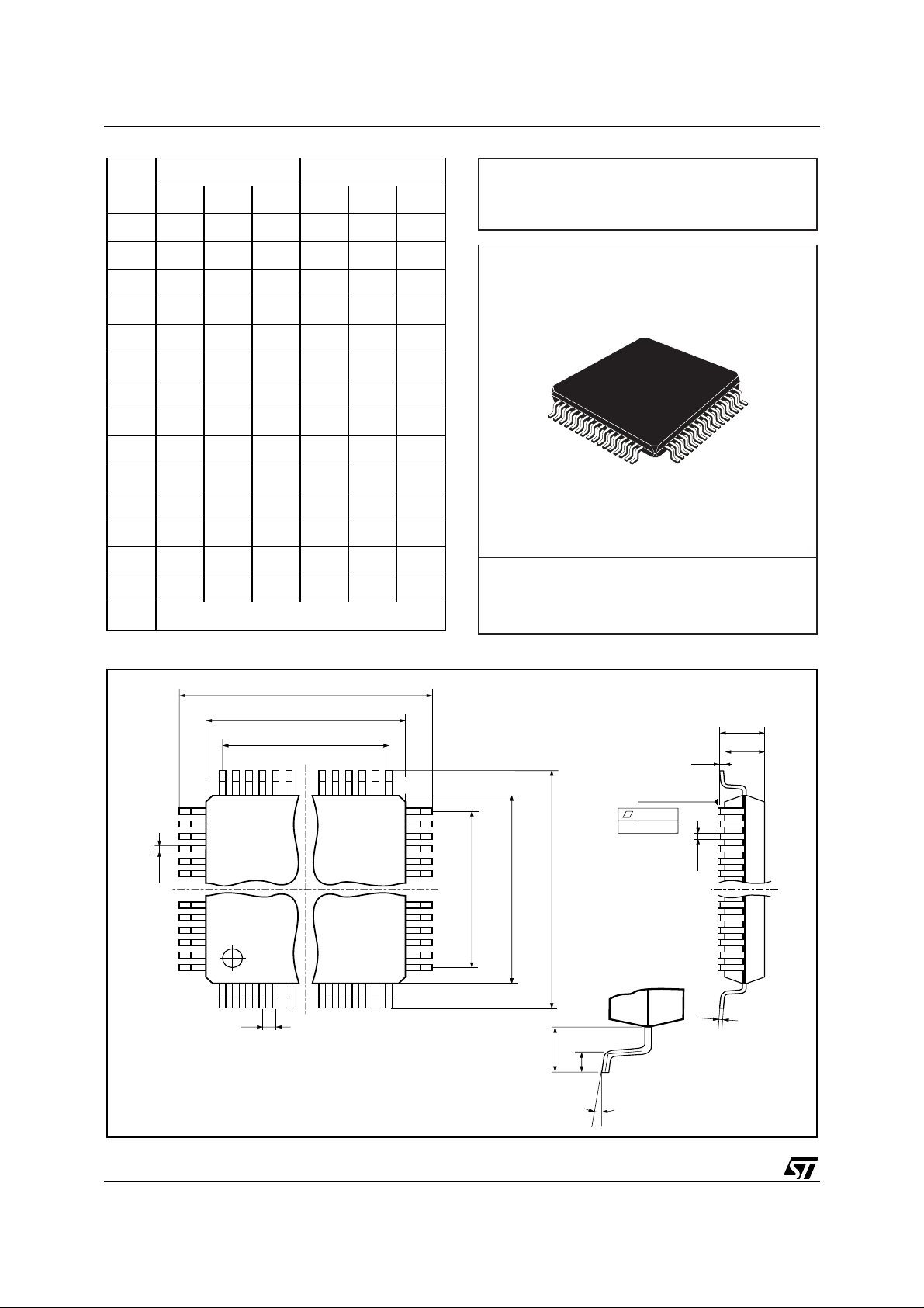
TDA7580
DIM.
mm inch
MIN. TYP. MAX. MIN. TYP. MAX.
A 1.60 0.063
A1 0.05 0.15 0.002 0.006
A2 1.35 1.40 1.45 0.053 0.055 0.057
B 0.18 0.23 0.28 0.007 0.009 0.011
C 0.12 0.16 0.20 0.0047 0.0063 0 .0079
D 12.00 0.472
D1 10.00 0.394
D3 7.50 0.295
e 0.50 0.0197
E 12.00 0.472
E1 10.00 0.394
E3 7.50 0.295
L 0.40 0.60 0.75 0.0157 0.023 6 0.0295
L1 1.00 0.0393
K 0°(min.), 7°(max.)
OUTLINE AND
MECHANICAL DATA
TQFP64
D
D1
A1
TQFP64
3348
32
E3D3E1
17
16
E
L1
L
0.10mm
Seating Plane
B
K
49
B
64
1
e
A
A2
C
30/31

TDA7580
Information furnished is believed to be accurate and reliable. However, STMicroelectronics assumes no responsibility for the consequences
of use of such information nor for any infringement of patents or other rights of third parties which may result from its use. No license is granted
by implic ation or otherwise unde r any patent or patent rights of STMicroelectroni cs. Specifications me ntioned in th i s publication are subject
to change without notice. This publication supersedes and replaces all information previously supplied. STMicroelectronics produ ct s are not
authorized for use as crit i cal component s in l i fe support dev i ces or systems without express written approval of STMic roelectronics.
The ST logo is a registered trademark of STMicroelectronics
2002 STMi croelectroni cs - All Rights Reserved
Australia - Brazil - Canada - China - F i nl and - France - Germany - Hong K ong - India - Israel - Italy - Japan -M alaysia - Mal ta - Morocco -
Singap ore - Spain - Sweden - Switzerl and - United Ki ngdom - United S tates.
STMicroelectronics GROUP OF COMPANIES
http://www.s t. com
31/31
 Loading...