

TDA7563
MULTIFUNCTION QUAD POWER AMPLIFIER
WITH BUILT-IN DIAGNOSTICS FEATURES
■ DMOS POWER OUTPUT
■ NON-SWITCHING HI-EFFICIENCY
■ HIGH OUTPUT POWER CAPABILITY 4x28W/
4Ω @ 14.4V, 1KHZ, 10% THD, 4x40W EIAJ
■ MAX. OUTPUT POWER 4x72W/2Ω
■ FULL I
2
C BUS DRIVING:
–ST-BY
– INDEPENDENT FRONT/REAR SOFT PLAY/
MUTE
– SELECTABLE GAIN 30dB
– 16dB (FOR LOW NOISE LINE OUTPUT
FUNCTION)
– HIGH EFFICIENCY ENABLE/DISABLE
2
–I
C BUS DIGITAL DIAGNOSTICS
■ FULL FAULT PROTECTION
■ DC OFFSET DETECTION
■ FOUR INDEPENDENT SHORT CIRCUIT
PROTECTION
■ CLIPPING DETECTOR PIN WITH
SELECTABLE THRESHOLD (2%/10%)
■ ST-BY/MUTE PIN
■ LINEAR THERMAL SHUTDOWN
■ ESD PROTECTION
MULTIPOWER BCD TECHNOLOGY
MOSFET OUTPUT POWER STAGE
FLEXIWATT27
ORDERING NUMBER: TDA7563
DESCRIPTION
The TDA7563 is a new BCD technology Quad
Bridge type of car radio amplifier in Flexiwatt27
package specially intended for car radio applications. Thanks to the DMOS output stage the
TDA7563 has a very low distortion allowing a clear
powerful sound. Among the features, its superior
efficienc y perform ance com ing from the i nternal ex clusive structure, makes it the m os t s ui t abl e device
to simplify the thermal management in high power
sets.The dissipated output power under average
listening condition is in fact reduced up to 50%
when compared to the level provided by conventional class AB solutions.This device is equipped
with a full diagnostics array that communicates the
status of each speaker through the I
2
C bus.
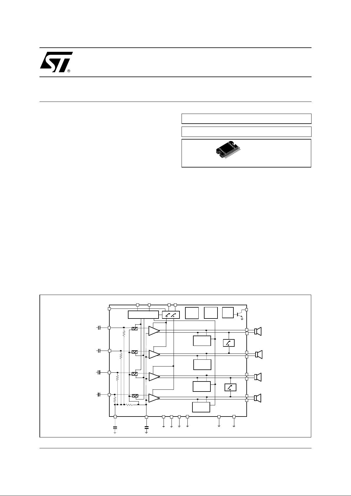
BLOCK DIAGRAM
ST-BY/MUTE
May 2003
IN RF
IN RR
IN LF
IN LR
SVR
CLK
DATA
VCC1 VCC2
Thermal
I2CBUS
Mute1 Mute2
F
R
F
R
AC_GND
16/30dB
16/30dB
16/30dB
16/30dB
RF
RR
PW_GND
Protection
& Dump
LF LR
Reference
Short Circuit
Protection &
Diagnostic
Short Circuit
Protection &
Diagnostic
Short Circ uit
Protection &
Diagnostic
Short Circuit
Protection &
Diagnostic
TAB
Clip
Detector
CD_OUT
OUT RF+
OUT RFOUT RR+
OUT RR-
OUT LF+
OUT LFOUT LR+
OUT LR-
S_GND
1/20
TDA7563
0
ABSOLUTE MAXIMUM RATINGS
Symbol Parameter Value Unit
V
op
V
V
peak
V
CK
V
DATA
I
O
I
O
P
tot
T
stg
THERMAL DATA
Symbol Parameter Value Unit
R
th j-case
Operating Supply Voltage 18 V
DC Supply Voltage 28 V
S
Peak Supply Voltage (for t = 50ms) 50 V
CK pin Voltage 6 V
Data Pin Voltage 6 V
Output Peak Current (not repetitive t = 100ms) 8 A
Output Peak Current (repetitive f > 10Hz) 6 A
Power Dissipation T
= 70°C 85 W
case
, TjStorage and Junction Temperature -55 to 150 °C
Thermal Resistance Junction to case
Max.
1 °C/W
PIN CONNECTION
(Top view)
27
26
25
24
23
22
21
20
19
18
17
16
15
14
13
12
11
10
9
8
7
6
5
4
3
2
1
TAB
DATA
PW_GND RR
OUT RRCK
OUT RR+
V
CC2
OUT RFPW_GND RF
OUT RF+
AC GND
IN RF
IN RR
S_GND
IN LR
IN LF
SVR
OUT LF+
PW_GND LF
OUT LFV
CC1
OUT LR+
CD-OUT
OUT LRPW_GND LR
STBY
TAB
D00AU123
2/20
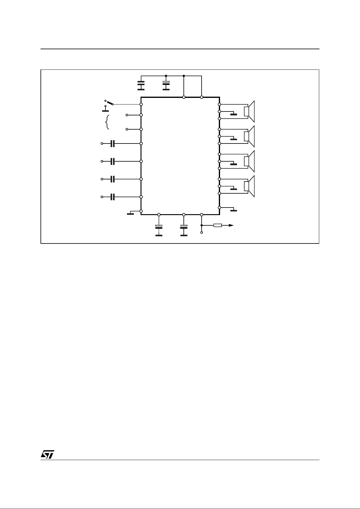
Figure 1. Application Circuit
TDA7563
V(4V .. V
I2C BUS
IN RF
IN RR
IN LF
IN LR
)
CC
DATA
CLK
C1 0.22µF
C2 0.22µF
C3 0.22µF
C4 0.22µF
C8
0.1µF
S-GND
C7
3300µF
2
26
23
16
15
12
13
14
C5
1µF
Vcc1 Vcc2
17 11 5
C6
10µF
721
18
19
20
22
25
24
10
9
8
6
3
4
1, 27
47K
CD OUT
+
+
+
+
TAB
OUT RF
OUT RR
OUT LF
OUT LR
V
D00AU1231A
3/20

TDA7563
ELECTRICAL CHARACTERISTICS
(Refer to the test circuit, V
= 14.4V; RL = 4Ω; f = 1KHz; GV = 30dB; T
S
= 25°C; unless otherwise specified.)
amb
Symbol Parameter Test Condition Min. Typ. Max. Unit
POWER AMPLIFIER
V
P
THD Total Harmonic Distortion P
Supply Voltage Range 8 18 V
S
Total Quiescent Drain Current 170 300 mA
I
d
Output Power EIAJ (VS = 13.7V) 35 40 W
O
THD = 10%
THD = 1%
= 2Ω; EIAJ (VS = 13.7V)
R
L
RL = 2Ω; THD 10%
R
= 2Ω; THD 1%
L
RL = 2Ω; MAX POWER
= 1W to 10W; STD MODE
O
HE MODE; PO = 1.5W
HE MODE; PO = 8W
= 1-10W, f = 10kHz 0.2 0.5 %
P
O
= 16dB; STD Mode
G
V
25 28
22
55
40
62
46
35
72
0.03
0.02
0.15
0.02 0.05 %
0.1
0.1
0.5
VO = 0.1 to 5VRMS
C
R
G
∆G
G
∆G
E
E
Cross Talk f = 1KHz to 10KHz, Rg = 600Ω 50 60 dB
T
Input Impedance 60 100 130 KΩ
IN
Voltage Gain 1 29.5 30 30.5 dB
V1
Voltage Gain Match 1 -1 1 dB
V1
Voltage Gain 2 15.5 16 16.5 dB
V2
Voltage Gain Match 2 -1 1 dB
V2
Output Noise Voltage 1 Rg = 600Ω 20Hz to 22kHz 50 100 mV
IN1
Output Noise Voltage 2 Rg = 600Ω; GV = 16dB
IN2
15 30 mV
20Hz to 22kHz
SVR Supply Voltage Rejection f = 100Hz to 10kHz; V
R
= 600Ω
g
= 1Vpk;
r
50 60 dB
BW Power Bandwidth 100 KHz
A
I
A
V
V
T
T
V
V
V
I
CD
CD
CD
Stand-by Attenuation 90 110 dB
SB
Stand-by Current 2 20 µ A
SB
Mute Attenuation 80 100 dB
M
Offset Voltage Mute & Play -100 0 100 mV
OS
Min. Supply Mute Threshold 7 7.5 8 V
AM
Turn ON Delay D2/D1 (IB1) 0 to 1 5 20 ms
ON
Turn OFF Delay D2/D1 (IB1) 1 to 0 5 20 ms
OFF
St-By/Mute pin for St-By 0 1.5 V
SBY
St-By/Mute pin for Mute 3.5 5 V
MU
St-By/Mute pin for Operating 7 V
OP
St-By/Mute pin Curren t V
MU
Clip Det High Leakage Current CD off 0 15 µA
LK
Clip Det Sat. Voltage CD on; ICD = 1mA 300 mV
SAT
Clip Det THD level D0 (IB1) = 1 5 10 15 %
THD
STBY/MUTE
V
STBY/MUTE
= 8.5V 20 4 0 µA
< 1.5V 0 10 µ A
S
W
W
W
W
W
W
%
%
%
V
4/20
TDA7563
ELECTRICAL CHARACTERISTICS
(Refer to the test circuit, V
= 14.4V; RL = 4Ω; f = 1KHz; GV = 30dB; T
S
(continued)
= 25°C; unless otherwise specified.)
amb
Symbol Parameter Test Condition Min. Typ. Max. Unit
D0 (IB1) = 0 1 2 3 %
TURN ON DIAGNOSTICS 1 (Power Amplifier Mode)
Pgnd Short to GND det. (below this
Power Amplifier in st-by 1.2 V
limit, the Output is considered in
Short Circuit to GND)
Pvs Short to Vs det. (above this limit,
Vs -1.2 V
the Output isconsidered in Short
Circuit to VS)
Pnop Normal operation
1.8 Vs -1.8 V
thresholds.(Within these limits,
the Output is considered without
faults).
Lsc Shorted Load det. 0.5 Ω
Lop O pen Load det. 130 Ω
Lnop Normal Load det. 1.5 70 Ω
TURN ON DIAGNOSTICS 2 (Line Driver Mode)
Pgnd Short to GND det. (below this
Power Amplifier in st-by 1.2 V
limit, the Output is considered in
Short Circuit to GND)
Pvs Short to Vs det. (above this limit,
Vs -1.2 V
the Output isconsidered in Short
Circuit to VS)
Pnop Normal operation
1.8 Vs -1.8 V
thresholds.(Within these limits,
the Output is considered without
faults).
Lsc Shorted Load det. 1.5 Ω
Lop O pen Load det. 400 Ω
Lnop Normal Load det. 4.5 200 Ω
PERMANENT DIAGNOSTICS 2 (Power Amplifier Mode or Line Driver Mode)
Pgnd Short to GND det. (below this
limit, the Output is considered in
Short Circuit to GND)
Pvs Short to Vs det. (above this limit,
Power Amplifier in Mute or Play,
one or more short circuits
protection activated
1.2 V
Vs -1.2 V
the Output is considered in Short
Circuit to VS)
Pnop Normal operation thresholds.
1.8 Vs -1.8 V
(Within these limits, the Output is
considered witho ut faults).
L
Shorted Load Det. Pow. Amp. mode 0.5 Ω
SC
Line Driver mode 1.5 Ω
V
Offset Detection Power Amplifier in play,
O
±1.5 ±2 ±2.5 V
AC Input signals = 0
I2C BUS INTERFACE
S
V
V
Clock Frequency 400 KHz
CL
Input Low Voltage 1.5 V
IL
Input High Voltage 2.3 V
IH
5/20

TDA7563
)
(V)
(W)
(W)
(W)
Figure 2. Quiescent Current vs. Supply Voltage
Id (mA)
250
230
210
190
170
150
130
110
90
70
Vin = 0
NO LOADS
8 1012141618
Vs (V)
Figure 3. Output Power vs. Supply Voltage (4Ω)
Po (W)
70
65
60
55
50
45
40
35
30
25
20
15
10
5
RL = 4 Ohm
f = 1 KHz
8 9 10 11 12 13 14 15 16 17 18
Vs (V
Po-max
THD = 10 %
THD = 1 %
Figure 5.
10
1
0.1
0.01
0.1 1 10
Figure 6.
10
1
0.1
0.01
0.001
Distortion vs. Output Power (4Ω, STD)
THD (%)
STANDARD MODE
Vs = 14.4 V
RL = 4 Ohm
f = 10 KHz
f = 1 KHz
Po
Distortion vs. Output Power (4Ω, HI-EFF)
THD (%)
HI-EFF MODE
Vs = 14.4 V
RL = 4 Ohm
f = 10 KHz
f = 1 KHz
0.1 1 10
Po
Figure 4. Output Power vs. Supply Voltage (2Ω)
Po (W)
100
90
80
70
60
50
40
30
20
10
RL = 2 Ohm
f = 1 KHz
8 9 10 11 12 13 14 15 16
Vs
6/20
Po-max
THD = 10 %
THD = 1 %
Figure 7.
10
1
0.1
0.01
0.1 1 10
Distortion vs. Output Power (2Ω, STD)
THD (%)
HI-EFF MODE
Vs = 14.4 V
RL = 2 Ohm
f = 10 KHz
f = 1 KHz
Po
 Loading...