


TDA7560
4 x 45WQUAD BRIDGE CAR RADIO AMPLIFIER PLUS HSD
PRODUCT PREVIEW
SUPERIOROUTPUTPOWER CAPABILITY:
4 x50W/4Ω MAX.
4 x45W/4ΩEIAJ
4 x30W/4Ω@ 14.4V,1KHz, 10%
4 x80W/2Ω MAX.
4 x77W/2Ω EIAJ
4 x55W/2Ω @ 14.4V,1KHz, 10%
EXCELLENT2ΩDRIVINGCAPABILITY
HI-FICLASS DISTORTION
LOW OUTPUT NOISE
ST-BYFUNCTION
MUTEFUNCTION
AUTOMUTEAT MIN. SUPPLYVOLTAGE DE-
TECTION
LOW EXTERNAL COMPONENTCOUNT:
– INTERNALLYFIXED GAIN(26dB)
– NOEXTERNALCOMPENSATION
– NOBOOTSTRAPCAPACITORS
ON BOARD0.35A HIGHSIDE DRIVER
PROTECTIONS:
OUTPUT SHORT CIRCUIT TO GND, TO V
ACROSS THELOAD
VERYINDUCTIVE LOADS
OVERRATING CHIP TEMPERATURE WITH
SOFT THERMAL LIMITER
LOADDUMP VOLTAGE
MULTIPOWER BCD TECHNOLOGY
MOSFETOUTPUT POWER STAGE
FLEXIWATT25
ORDERING NUMBER: TDA7560
FORTUITOUSOPEN GND
REVERSEDBATTERY
ESD
DESCRIPTION
The TDA7560 is a breakthrough BCD (Bipolar /
CMOS / DMOS) technology class AB Audio
Power Amplifier in Flexiwatt 25 package designed
for high power car radio
,
S
The fullycomplementaryP-Channel/N-Channel
output structure allowsa rail to rail outputvoltage
swingwhich, combined with high output current
and minimised saturation losses sets new power
referencesin the car-radiofield, with unparalleleddistortion performances.
BLOCK AND APPLICATION DIAGRAM
Vcc1 Vcc2
ST-BY
MUTE
IN1
0.1µF
IN2
0.1µF
IN3
0.1µF
IN4
0.1µF
AC-GND
0.47µF47µF
SVR TAB S-GND
HSDHSD
OUT1+
OUT1PW-GND
OUT2+
OUT2PW-GND
OUT3+
OUT3PW-GND
OUT4+
OUT4PW-GND
D94AU158B
November 1999
This is preliminary information on a new productnow in development. Details are subject to change without notice.
100nF470µF
1/10
TDA7560
ABSOLUTE MAXIMUM RATINGS
Symbol Parameter Value Unit
V
CC
V
CC (DC)
V
CC (pk)
I
O
P
tot
T
j
T
stg
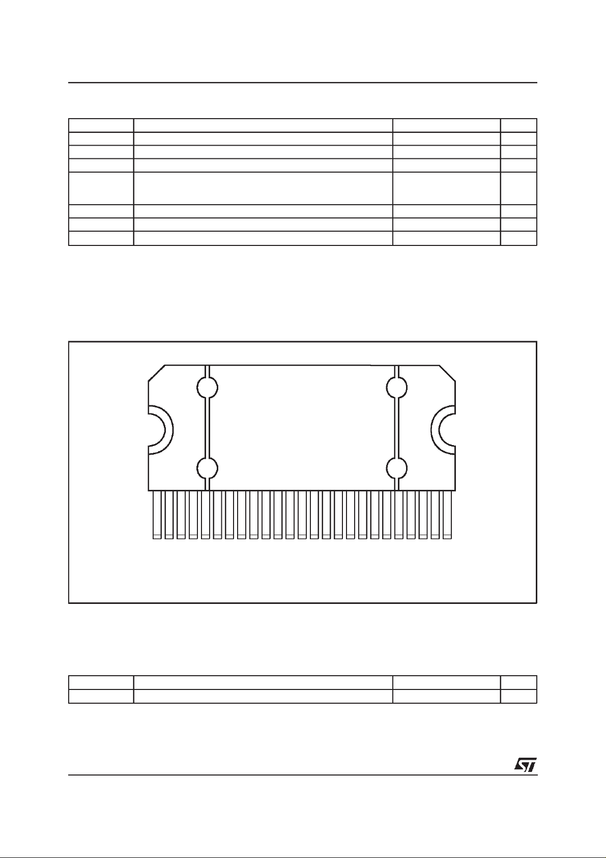
PIN CONNECTION(Topview)
Operating Supply Voltage 18 V
DC Supply Voltage 28 V
Peak Supply Voltage (t = 50ms) 50 V
Output Peak Current:
Repetitive (Duty Cycle 10% at f = 10Hz)
Non Repetitive (t = 100µs)
Power dissipation, (T
=70°C) 80 W
case
9
10
Junction Temperature 150
Storage Temperature – 55 to150 °C
A
A
C
°
1 25
TAB
OUT2-
P-GND2
ST-BY
CC
V
OUT2+
OUT1-
P-GND1
SVR
OUT1+
IN1
IN2
IN4
S-GND
IN3
OUT3+
AC-GND
OUT3-
P-GND3
CC
V
MUTE
OUT4+
D94AU159A
OUT4-
P-GND4
HSD
THERMAL DATA
Symbol Parameter Value Unit
Thermal Resistance Junction to Case Max. 1
2/10
R
th j-case
C/W
°
TDA7560
ELECTRICALCHARACTERISTICS(VS= 13.2V;f = 1KHz; Rg= 600Ω;RL=4Ω;T
amb
=25°C;
Refer to the test and application diagram,unless otherwisespecified.)
Symbol Parameter Test Condition Min. Typ. Max. Unit
V
dV
I
q1
OS
OS
Quiescent Current RL=
∞
Output Offset Voltage Play Mode
During mute ON/OFF output
120 200 320 mA
80 mV
±
80 mV
±
offset voltage
G
v
dG
P
o
P
o EIAJ
P
o max.
THD Distortion P
e
No
SVR Supply Voltage Rejection f = 100Hz; V
f
ch
R
C
T
I
SB
I
pin4
V
SB out
V
SB in
A
M
V
M out
V
Min
V
AM in
Voltage Gain 25 26 27 dB
Channel Gain Unbalance ±1dB
v
Output Power VS= 13.2V; THD = 10%
V
= 13.2V; THD = 1%
S
V
= 14.4V; THD = 10%
S
V
= 14.4V; THD = 1%
S
V
= 13.2V; THD = 10%, 2Ω
S
V
= 13.2V; THD = 1%, 2
S
V
= 14.4V; THD = 10%, 2Ω
S
V
= 14.4V; THD = 1%, 2Ω
S
EIAJ Output Power(*) VS= 13.7V; RL=4Ω
V
= 13.7V; RL=2
S
Max. Output Power (*) VS= 14.4V; RL=4
V
= 14.4V; RL=2Ω
S
=4W
o
P
= 10W; RL=2
o
Ω
Ω
Ω
Output Noise ”A” Weighted
Bw = 20Hz to 20KHz
= 1Vrms 50 70 dB
r
23
16
28
20
42
Ω
32
50
40
41
75
25
19
30
23
45
34
55
43
45
77
50
80
0.006
0.015
35
50
0.05
0.07
50
70
High Cut-Off Frequency PO= 0.5W 100 300 KHz
Input Impedance 80 100 120 KΩ
i
Cross Talk f = 1KHz PO=4W
St-By Current Consumption V
f = 10KHz P
= 1.5V 75
St-By
O
=4W
60 70
60
–
–
St-by pin Current VSt-By = 1.5V to 3.5V ±10 µA
St-By Out ThresholdVoltage (Amp: ON) 3.5 V
St-By in Threshold Voltage (Amp: OFF) 1.5 V
Mute Attenuation P
=4W 80 90 dB
Oref
Mute Out ThresholdVoltage (Amp: Play) 3.5 V
Mute In Threshold Voltage (Amp: Mute) 1.5 V
VSAutomute Threshold (Amp: Mute)
Att≥80dB; P
Oref
=4W
6.5 7
(Amp: Play)
I
pin22
Muting Pin Current V
Att < 0.1dB; P
= 1.5V
MUTE
= 0.5W
O
7.5 8
71218
(Sourced Current)
V
= 3.5V -5 18 µA
MUTE
HSD SECTION
V
dropout
I
prot
(*) Saturated square wave output.
Dropout Voltage IO= 0.35A; VS= 9 to16V 0.25 0.6 V
Current Limits 400 800 mA
W
W
W
W
W
W
W
W
W
W
W
W
%
%
V
µ
µV
dB
dB
A
µ
V
V
A
µ
3/10

TDA7560
Figure 1: Standard Test andApplication Circuit
ST-BY
MUTE
IN1
IN2
IN3
IN4
R1
10K
R2
47K
C1
0.1µF
C2 0.1µF
C3 0.1µF
C4 0.1µF
C9
1µF
C10
1µF
S-GND
0.1µF
4
22
11
12
15
14
13
C5
0.47µF
C8
16 10 25 1
C7
2200µF
Vcc1-2 Vcc3-4
620
SVR TAB
C6
47µF
HSD
9
8
7
5
2
3
17
18
19
21
24
23
OUT1
OUT2
OUT3
OUT4
D95AU335B
4/10

Figure 2: P.C.B. and componentlayout of thefigure 1 (1:1scale)
COMPONENTS &
TOP COPPER LAYER
TDA7560
BOTTOM COPPER LAYER
5/10

TDA7560
Figure 3. Quiescentcurrent vs. supply
voltage.
Id(mA)
240
220
Vi= 0
RL = 4 Ohm
200
180
160
140
8 1012141618
Vs (V)
Figure 5. Outputpower vs. supplyvoltage.
Po(W)
13 0
12 0
Po-m ax
11 0
10 0
90
80
RL= 2 Ohm
f=1KHz
THD =10%
70
60
50
40
THD =1%
30
20
10
8 9 10 11 12 13 14 15 16 17 18
Vs(V)
Figure4. Output powervs. supply voltage.
Po(W)
80
75
70
Po-max
65
60
RL=4Ohm
55
f=1KHz
50
THD=10%
45
40
35
30
25
20
THD=1%
15
10
5
8 9 10 11 12 13 14 15 16 17 18
Vs(V)
Figure6. Distortion vs.output Power
TH D(%)
10
Vs=14.4 V
1
RL=4 Ohm
f=10KHz
0.1
0.01
0.001
0.1 1 10
f=1 KHz
Po(W)
Figure 7. Distortion vs. output power
TH D(%)
10
Vs=14.4 V
RL=2 Ohm
1
f=10KHz
0.1
0.0 1
0.00 1
0.1 1 10
6/10
f=1 KHz
Po (W)
Figure8. Distortion vs.frequency.
THD(%)
10
Vs= 14.4V
1
RL=4 Ohm
Po = 4 W
0.1
0.01
0.001
10 100 1000 10000
f(Hz)

TDA7560
Figure 9. Distortion vs. frequency.
TH D(%)
10
Vs=14.4V
1
RL= 2Ohm
Po= 8 W
0.1
0.01
0.001
10 100 1000 10000
f(Hz)
Figure 11. Supply voltage rejection vs. fre-
quency.
SVR(dB)
100
90
80
70
60
Figure10. Crosstalk vs. frequency.
CROSSTALK(dB)
90
80
70
60
50
RL= 4Ohm
Po=4 W
40
Rg= 600Ohm
30
20
10 100 1000 10000
f(Hz)
Figure12. Output attenuation vs. supply
voltage.
OUTA T TN(dB)
0
-20
-40
RL= 4 Ohm
Po=4 Wref.
50
Rg= 600 Ohm
40
Vripple=1Vrms
30
20
10 100 100 0 1000 0
f(Hz)
Figure 13. Output noise vs. source resistance.
En(uV)
130
120
Vs=14.4V
110
RL=4Ohm
100
90
80
70
60
50
40
30
20
1 10 100 1000 10000 100000
22-22KHzlin.
”A”wgtd
Rg(Ohm)
-60
-80
-100
5678910
Vs(V)
Figure14. Power dissipation& efficiencyvs.
output power (sine-waveoperation)
Ptot(W)
90
80
Vs=13.2V
70
RL=4 x4 Ohm
60
f=1 KHzSINE
50
40
30
20
10
0
024681012141618202224262830
Po(W)
n
Ptot
n(%)
90
80
70
60
50
40
30
20
10
0
7/10

TDA7560
Figure 15. Power dissipationvs. ouput power
(Music/SpeechSimulation)
Ptot(W)
30
Vs=13.2V
25
RL=4 x 4Ohm
GAUSSIANNOISE
20
15
10
5
0123456
CLIP START
Po(W)
APPLICATIONHINTS (ref.to the circuit of fig. 1)
SVR
Besides its contributionto the ripple rejection, the
SVR capacitor governs the turn ON/OFF time sequence and, consequently,playsan essentialrole
in the pop optimization during ON/OFF transients.To conveniently serve both needs, ITS
MINIMUM RECOMMENDEDVALUE IS 10µF.
Figure16. Power dissipationvs. output power
(Music/SpeechSimulation)
Ptot(W)
60
Vs= 13.2V
55
RL=4 x 2 Ohm
GAUSSIANNOISE
50
45
40
35
30
25
20
15
10
5
0246810
CLIP START
Po(W)
be employed to drive muting and stand-bypins in
absence of trueCMOS ports or microprocessors.
R-C cells have always to be used in order to
smooth down the transitions for preventing any
audibletransient noises.
About the stand-by, the time constant to be assigned in order to obtain a virtually pop-free transitionhas to be slowerthan 2.5V/ms.
INPUT STAGE
The TDA7560’sinputs are ground-compatibleand
can stand very high input signals (± 8Vpk)without
any performancesdegradation.
If the standard value for the input capacitors
(0.1µF) is adopted, the low frequency cut-off will
amount to 16 Hz.
STAND-BYAND MUTING
STAND-BY and MUTING facilities are both
CMOS-COMPATIBLE. If unused, a straight connection to Vs of their respectivepins would be admissible. Conventionallow-power transistorscan
HEATSINKDEFINITION
Under normal usage (4 Ohm speakers) the
heatsink’s thermal requirements have to be deduced from fig. 15, which reports the simulated
power dissipation when real music/speech programmes are played out. Noise with gaussiandistributedamplitude was employed for this simulation. Based on that, frequent clipping occurence
(worst-case) will cause Pdiss = 26W. Assuming
Tamb = 70°C and T
= 150°C as boundary
CHIP
conditions, the heatsink’s thermal resistance
should be approximately2°C/W. This would avoid
any thermal shutdown occurence even after longterm andfull-volume operation.
8/10

TDA7560
DIM.
MIN. TYP. MAX. MIN. TYP. MAX.
mm inch
A 4.45 4.50 4.65 0.175 0.177 0.183
B 1.80 1.90 2.00 0.070 0.074 0.079
C 1.40 0.055
D 0.75 0.90 1.05 0.029 0.035 0.041
E 0.37 0.39 0.42 0.014 0.015 0.016
F (1) 0.57 0.022
G 0.80 1.00 1.20 0.031 0.040 0.047
G1 23.75 24.00 24.25 0.935 0.945 0.955
H (2) 28.90 29.23 29.30 1.138 1.150 1.153
H1 17.00 0.669
H2 12.80 0.503
H3 0.80 0.031
L (2) 22.07 22.47 22.87 0.869 0.884 0.904
L1 18.57 18.97 19.37 0.731 0.747 0.762
L2 (2) 15.50 15.70 15.90 0.610 0.618 0.626
L3 7.70 7.85 7.95 0.303 0.309 0.313
L4 5 0.197
L5 3.5 0.138
M 3.70 4.00 4.30 0.145 0.157 0.169
M1 3.60 4.00 4.40 0.142 0.157 0.173
N 2.20 0.086
O 2 0.079
R 1.70 0.067
R1 0.5 0.02
R2 0.3 0.12
R3 1.25 0.049
R4 0.50 0.019
V5°(Typ.)
V1 3°(Typ.)
V2 20°(Typ.)
V3 45°(Typ.)
(1): dam-bar protusion notincluded
(2): molding protusion included
OUTLINE AND
MECHANICALDATA
Flexiwatt25
L2
H
V3
OL3 L4
V
C
H3
G
H1
G1
R3
H2
F
A
R4
N
V2
R2
R
L
L1
V1
R2
B
V
FLEX25ME
R1
L5
V1
R1 R1
E
M1
M
D
9/10

TDA7560
Information furnished is believed to be accurate and reliable. However, STMicroelectronics assumes no responsibility for the consequences
of use of such information nor for any infringement of patents or other rights of third parties which may result from its use. No license is
granted by implication or otherwise under any patent or patent rights of STMicroelectronics. Specification mentioned in this publication are
subject to change without notice. This publication supersedes and replaces all information previously supplied. STMicroelectronics products
are not authorized for use as critical components in lifesupport devices or systems without express written approval of STMicroelectronics.
The ST logo is a registered trademark of STMicroelectronics
1999 STMicroelectronics – Printed in Italy – AllRights Reserved
STMicroelectronics GROUPOF COMPANIES
Australia - Brazil - China- Finland - France - Germany - Hong Kong - India - Italy - Japan - Malaysia - Malta- Morocco -
Singapore - Spain - Sweden - Switzerland -United Kingdom - U.S.A.
http://www.st.com
10/10
 Loading...