

TDA7550/R TDA7551
®
DIGITAL SIGN AL PROCESS IN G IC FOR SPEE CH AND
24-BIT, FIXED POINT, 50 MIPS DSP CORE
LARGE ON-BOARD PROGRAM ROM AND
DATA RAM (UP TO 16Kw ROM/RAM AND
16Kw RAM)
INTEGRAT ED ST EREO A/D AND D/A, 16 -BI T
SIGMA-DELTA
PROGRAMMABLE CODEC SAMPLE RATE
FROM 4 TO 48 kHz
ON-BOARD PLL FOR CORE CLOCK AND
CONVERTERS
MANAGEMENT OF EXTERNAL
FLASH/ SRAM/DR AM MEMORY BANK
I2C OR SPI SERIAL INTERFACE FOR EXTERNAL CONTROL
80-PIN TQFP, 0.65 mm PITCH
AUTOMOTIVE GRADE (FROM -40° C to
+85°C)
DESCRIPTION
The TDA755X family is a high performances, fully
programmable 24-bit, 50 MIPS Digital Signal
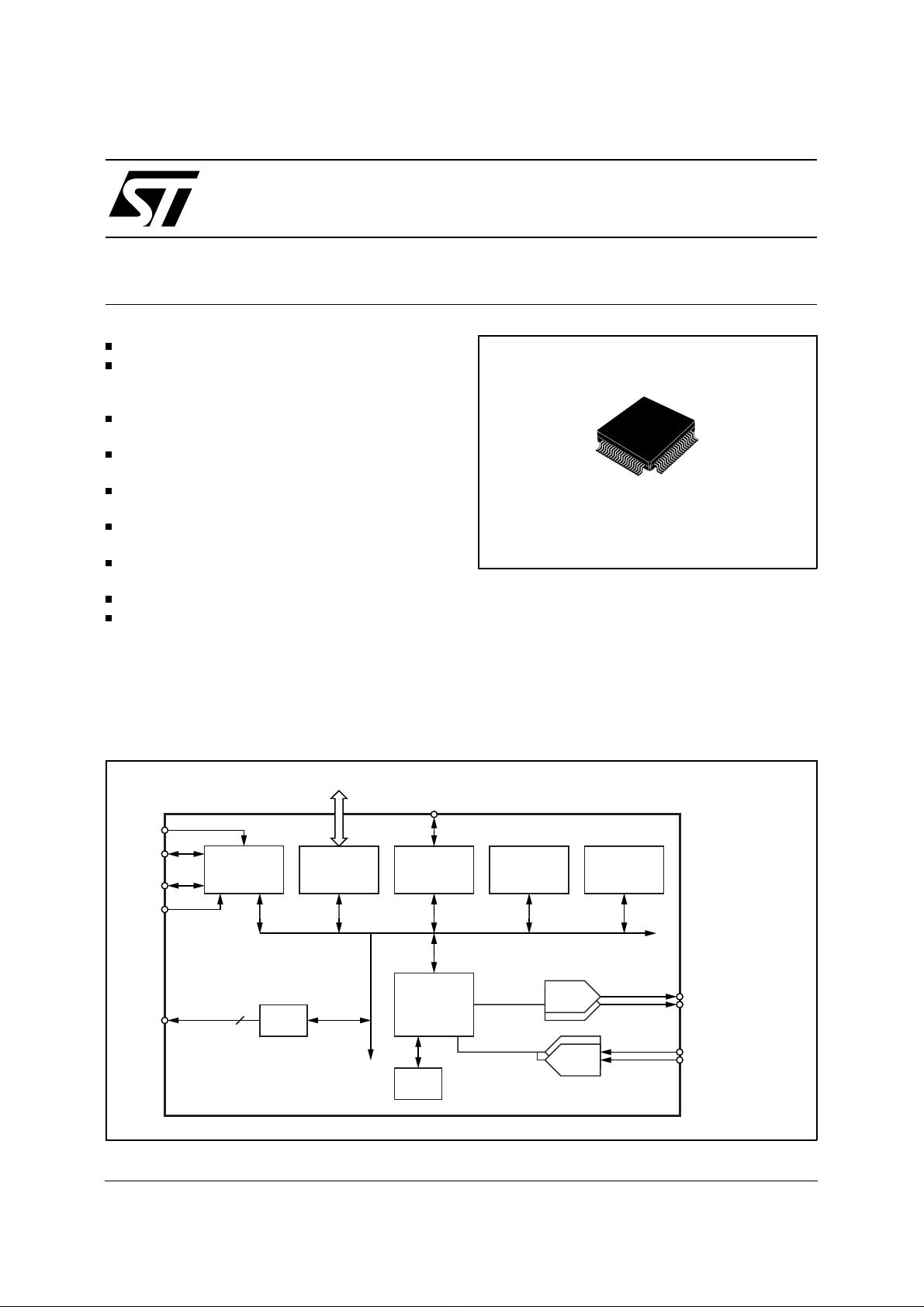
BLOCK DIAGRAM
TDA7552 TDA7553
AUDIO APPLICATIO NS
PRODUCT PREVIEW
TQFP80
Processor (DSP), designed to support several
speech and audio applications, as Automatic
Speech Recognition, Speech Synthesis, Speaker
Verification, Echo and Noise Cancellation. Software for these applications is licenced by Lernout
& Hauspie and NCTI.
It offers an effective solution for this kind of applications because of the A/D and D/A converters
and the big amount of memory integrated on chip.
MULTIPLEXED BUS
I2C/SPI
PORT
8
FLAGS
September 1999
This is preliminary information on a new product now in development. Details are subject to change without notice.
FLASH
INTERFACE
SAI ROM/RAM
DSP
CORE
PLL
DAC
ADC
RAM
L
R
L
R
ANALOG OUT
ANALOG IN
D99AU1020A
1/12

TDA7550R - TDA7550 - TDA7551 - TDA7552 - TDA7553
APPLICATIONS
Real time digital speech and audio processing:
compression, echo cancelling, noise cancelling,
speaker verification.
speech recognition, speech synthesis, speech
ABSOLUTE MAXIMUM RATINGS
Symbol Parameter Value Unit
V
DDP
VD, V
T
T
P
IN
op
stg
tot
Pads DC Supply Voltage –0.3 to VDD +0.3 V
Digital or Analog Input Voltage –0.3 to V
+0.3 V
DDP
Operating Temperature Range –40 to +85 °C
Storage Temperature Range –55 to +150 °C
Total Maximum Power Dissipation mW
PIN CONNECTION
DRDN
GND
ALE
XTO
PGND
PVCC
XTI
CLKOUT
VDD
GPIO4
GPIO7
REFCAP
VREF
CVDDA
TEST4
60
59
58
57
56
55
54
53
52
51
50
49
48
47
46
45
44
43
42
41
CGNDA
VINL
VINR
GND
VDD
VOUTL
VOUTR
CVDD
CGND
GPIO3
GPIO6
GPIO2
GND
VDD
SDA/SS
SCL/SCK
INTN
NRESET
DBRQN
DBOUT
EMI_AD5
EMI_AD6
VDD
GND
EMI_AD7
EMI_A8
EMI_A7
EMI_A10
EMI_A11
EMI_A12
EMI_A13
EMI_A14
EMI_A15
VDD
GND
EMI_A16
EMI_A17
EMI_A18
EMI_A19
EMI_A20
EMI_AD3
EMI_AD4
79
80
1
2
3
4
5
6
7
8
9
10
12
13
14
15
16
17
18
19
20
21 22 23 24 25
EMI_AD2
77
78
EMI_AD0
EMI_AD1
76
75 74 73 72 7071 69 68 67 66 65
26 27 28 29 30
311132 33 34 35 36
64 63 62 61
37 38 39 40
2/12
DWRN
EMI_A21
TEST1
TEST2
MISO
MOSI
VDD
GND
SDI
TEST3
SCK
LRCK
VDD
GND
SDO
GPIO1
GPIO0
DBCK
GPIO5
DBIN
TQFP80
TDA7550R - TDA7550 - TDA7551 - TDA7552 - TDA7553
PIN FUNCTIONS
N. Name Type Description
1 EMI_AD5 I/O EMI Multiplexed Address/Data Line 5. these pin acts as the EMI multiplexed
2 EMI_AD6 I/O EMI Multiplexed Address/Data Line 6. these pin acts as the EMI multiplexed
3 VDD I Digital power supply
4 GND I Ground
5 EMI_AD7 I/O EMI Multiplexed Address/Data Line 7. these pin acts as the EMI multiplexed
6 EMI_A8 O EMI Address Line 8. these pin acts as the EMI address line 8. The interface is
7 EMI_A9 O EMI Address Line 9. these pin acts as the EMI address line 9.
8 EMI_A10 O EMI Address Line 10. these pin acts as the EMI address line 10.
9 EMI_A11 O EMI Address Line 11. these pin acts as the EMI address line 11.
10 EMI_A12 O EMI Address Line 12. these pin acts as the EMI address line 12.
11 EMI_A13 O EMI Address Line 13. these pin acts as the EMI address line 13.
12 EMI_A14 O EMI Address Line 14. these pin acts as the EMI address line 14.
13 EMI_A15 O EMI Address Line 15. these pin acts as the EMI address line 15.
14 VDD I Digital power supply
15 GND I Ground
16 EMI_A16 O EMI Address Line 16. these pin acts as the EMI address line 16.
17 EMI_A17 O EMI Address Line 17. these pin acts as the EMI address line 17.
18 EMI_A18 O EMI Address Line 18. these pin acts as the EMI address line 18.
19 EMI_A19 O EMI Address Line 19. these pin acts as the EMI address line 19.
20 EMI_A20 O EMI Address Line 20. these pin acts as the EMI address line 20.
21 EMI_A21 O EMI Address Line 21. these pin acts as the EMI address line 21.
22 DWRN O EMI Write Enable. This pin serves as the write enable for the EMI
23 TEST1 I Test 1. Used for test: set to LOW for normal operation
24 TEST2 I Test 2. Used for test: set to HIGH for normal operation
25 MISO I/O SPI Master Output Slave Input Serial Data. Serial Data Output for SPI type serial
26 MOSI I/O SPI Master Input Slave Output Serial Data. Serial Data Input for SPI type serial
27 VDD I Digital Power Supply
28 GND I Ground
29 TEST3 I Test 3. Used for test: set to LOW for normal operation
30 SDI I SAI Data Input
31 SCK I/O SAI Bit Clock
32 LRCK I/O SAI Left/Right Clock
33 VDD I Digital power supply
34 GND I Ground
35 SDO O SAI Data Output
address and data line 5
address and data line 6
address and data line 7
designed to address up to 4 Mbytes of External Flash, EPROM or SRAM.
Port when in SPI master Mode and Serial Data Input when in SPI Slave Mode
Port when in SPI master Mode and Serial Data Output when in SPI Slave Mode
3/12

TDA7550R - TDA7550 - TDA7551 - TDA7552 - TDA7553
PIN FUNCTIONS
N. Name Type Description
36 GPIO1 I/O General Purpose I/O
37 GPIO0 I/O General Purpose I/O
38 GPIO5 I/O General Purpose I/O
39 DBCK I/O Debug port Bit Clock/Chip Status 1. The serial clock for the Debug Port is
40 DBIN I/O Debug port Serial Input/Chip Status 0. The serial data input for the Debug Port is
41 DBOUT I/O Debug Port Serial Output. This pin is the serial Data output for the Debug port.
42 DBRQN I Debug Port Request Input. This pin is used to request Debug Mode operation to
43 NRESET I System Reset. A low level applied to RESET input initializes the IC.
44 INTN I External interrupt line. When this line is asserted low the DSP may be interrupted.
45 SCL/SCK I/O I
46 SDA/SS I/O I2C Serial Data Line. Data line for I2C bus. Schmitt trigger input.
47 VDD I Digital Power Supply
48 GND I Ground
49 GPIO2 I/O General Purpose I/O
50 GPIO6 I/O General Purpose I/O
51 GPIO3 I/O General Purpose I/O
52 CGND I Ground for the internal CODEC cell
53 CVDD I Power Supply for the internal CODEC cell
54 VOUTR O Single-ended right channel analogue output from DAC
55 VOUTL O Single-ended left channel analogue output from DAC
56 VDD I Digital power supply
57 GND I Ground
58 VINR I Single-ended right channel analogue input to ADC
59 VINL I Single-ended left channel analogue input to ADC
60 CGNDA I Ground for the internal CODEC cell
61 TEST4 O Connect a 22K pull-down resistor
62 CVDDA I Power Supply for the internal CODEC cell
63 VREF O Voltage Reference from the CODEC cell
64 REFCAP O Voltage Reference Capacitor Bypass
65 GPIO7 I/O General Purpose I/O
66 GPIO4 I/O General Purpose I/O
67 VDD I Digital power supply
68 CLKOUT O Clock Output. Output Clock divided down from PLL
(continued)
provided. May also be used as GPIO9.
provided. May also be used as GPIO11.
May also be used as GPIO10.
Euterpe
2
C Serial Clock Line. Clock line for I2C bus. Schmitt trigger input.
I/O SPI Bit Clock. If SPI interface is enabled, it behaves as SPI bit clock.
I SPI Slave Select. If SPI interface is enabled, it behaves as Slave select line for
SPI bus.
4/12

TDA7550R - TDA7550 - TDA7551 - TDA7552 - TDA7553
PIN FUNCTIONS
N. Name Type Description
69 XTI I Crystal Oscillator Input. Crystal Oscillator Input drive
70 PGND O PLL Ground Input. Ground connection for Oscillator circuit
71 PVCC I PLL Power Supply Positive. Supply for PLL Clock Oscillator
72 XTO O Crystal Oscillator Output. Crystal Oscillator Output drive
73 ALE O EMI Address Latch Enable. This pin acts as the EMI Address Latch Enable for the
74 GND I Ground
75 DRDN O EMI Read Enable. This pin serves as the read enable for the EMI
76 EMI_AD0 I/O EMI Multiplexed Address/Data Line 0. these pin acts as the EMI multiplexed
77 EMI_AD1 I/O EMI Multiplexed Address/Data Line 1. these pin acts as the EMI multiplexed
78 EMI_AD2 I/O EMI Multiplexed Address/Data Line 2. these pin acts as the EMI multiplexed
79 EMI_AD3 I/O EMI Multiplexed Address/Data Line 3. these pin acts as the EMI multiplexed
80 EMI_AD4 I/O EMI Multiplexed Address/Data Line 4. these pin acts as the EMI multiplexed
(continued)
External Memory Interface
address and data line 0
address and data line 1
address and data line 2
address and data line 3
address and data line 4
RECOMMENDED DC OPERATING CONDITIONS
Symbol Parameter Test Condition Min. Typ. Max. Unit
V
DD
T
J
Power Supply Volrage Range 3 3.3 3.6 V
Operating Junction Temp. –40 125 °C
5/12

TDA7550R - TDA7550 - TDA7551 - TDA7552 - TDA7553
24 BIT DSP CORE
The DSP Core is a general purpose 24-bit DSP.
The main feature of the DSP Core are listed below:
50Mhz Operating Frequency (50 MIPS)
Single cycle multiply and accumulate
2x56-bit Accumulators
Double precision multiply
Convergent rounding
Scaling and saturation arithmetic
48-bit or 2x24-bit parallel moves
64 interrupt vector locations
Fast or long interrupts possible
Programmable interrupt priorities and masking
8 each Address Registers, Address Offset
Registers and Address Modulo Registers
Linear, Reverse Carry, Multiple Buffer Modulo,
Multiple Wrap-around Modulo address arithmetic
Post-increment or decrement by 1 or by offset,
Index by offset, predecrement address
Repeat instruction and zero overhead DO
loops
Hardware stackcapable of nesting 7 DO loops
or 15 interrupts/subroutines
Bit manipulation instructions possible on all
registers and memory locations. Also Jump on
bit test.
Data Arithmetic Logic Unit (DALU)
Address Generation Unit (AGU)
Program Control Unit (PCU)
Three Data Buses
Three Address Buses
Internal Data Bus Switch
bit Manipulation Unit
Debug Logic
Memories
16384x24-bit Program ROM used for storing the
program code.
16384x24-bit Data RAM used for storing Data.
DSP peripherals
Serial Audio Interface (SAI)
The SAI is used to deliver digital audio to t he
DSP from an external source and to deliver
digital audio from the DSP to an external DAC.
It allows using an external CODEC. The main
features of this block are listed below:
– One Data Transmission Line
– One Data Reception Line
– Master and Slave Operating Modes
– Reference clock for transmission supplied
– Transmit and Receive Interrupt Logic
modified to trigger on Left/Right data pairs
– Receive and Transmit Data Registers have
two locations to hold left and right data
I2C interface/SPI
The inter integrated-circuit bus is a simple bidirectional two-wire bus used for efficient inter
IC control. All I
2
C bus compatible devices incorporate an on-chip interface which allows
them communicate directly with each via the
2
I
C bus.
Every component hoocked up to the I
has it’s own unique address whether it is a
CPU, memory or some other complex function
chip. Each of these chips can act as a receiver
and/or transmitter depending on it’s functionality.
The Serial Peripheral Interface (SPI) can be
enabled instead of the I
2
C interface. During an
SPI transfer, data is trasmitted and received
simulaneously. A serial clock line synchronizes
shifting and sampling of the information on the
two serial data lines. A slave select line allows
individual selection of a slve SPI device. When
an SPI transfer occurs an 8-bit word is shifted
out one data pin while another 8-bit character
is simultaneously shifted in a second data pin.
The central element in the SPI system is the
shift register and the read data buffer. The system is single buffered in the trasmit direction
and double buffered in the receive direction.
EMI
The External Memory Interface is viewed as a
memory mapped peripheral. Data transfers are
performed by moving data into/from data registers and the control is exercised by polling
status flags in the control/status register or by
servicing interrupts. An external memory write
is executed by writing data into the Data Write
register. An external memory read operation is
executed by either writing to the Offset register
or reading the Data read register, depending
on the configuration.
The main features of the EMI are listed below:
– Data bus width fixed at 4 bits for DRAM and
8 bits for SRAM
– 22 bit address bus multiplexed with an 8 bit
data bus
– Three choices of data word lenghths, 8, 16 or
24 bits in SRAM mode
– Two choices of data word lenght, 16 or 24
bits in DRAM mode
– Thirteen address lines 2
26
= 256Mbits
2
C bus
6/12

TDA7550R - TDA7550 - TDA7551 - TDA7552 - TDA7553
addressable DRAM
– Refresh rate for DRAM can be chosen
among sixteen divide factors
– SRAM or DRAM relative addressing modes
22
– 2
=4MBytes addressable SRAM
– Four SRAM Timing choices
– Two Read Offset Register
PLL
The Euterpe clock system generates the following clocks:
– DCLK the DSP core clock
– MCLK CODEC master clock
– LRCLK left/right clock for the SAI and
the CODEC
– SCLK shift seria l clo ck fo r th e SAI and
the CODEC
The output of the PLL operates from 70 to 140
MHz. The DSP core can operate with a clock
up to 50 MHz.
DEVICE versions
Part No.
TDA7550R RAM One of the
TDA7550 ROM Speech
TDA7551 Speaker
TDA7552 Text-To-
TDA7553 SF/FDE Master
Internal
Program
Memory
Function Serial I/F
below
Recognition
Verification
Speech
From the VCO output the audio clock are derived.
CODEC
The main features of the CODEC are listed below:
– one 16-bit Delta Sigma Stereo ADC
– 80 dB Dynamic Range
– Oversampling Ratio: 128
– one 16-bit Delta Sigma Stereo DAC
– 80 dB Dynamic Range
– Interpolating Ratio: 128
– Sampling rates of 4kHz to 48kHz
– Signal Noise Ratio: 80 dB Typ.
The analog interface is in the form of differential signals for each channel. The interface on
the digital side has the form of an SAI interface
and can interface directly to an SAI channel
and then to the DSP core.
External
Memory
Master or
2
Slave I
Slave I2C FLASH YES, 1
2
Slave I
2
Slave I
2
I
C or SPI
FLASH
C
or RAM
C Optional
FLASH
C – NO YES
(RAM) YES, 1
Audio
Input
YES
(by appl.)
(voice in)
YES, 1
(voice in)
(voice in)
Audio
Output
YES
(by appl.)
YES
(prompts)
YES
(prompts)
(voice out)
YES
(filtered)
Software
Custom
Specs.
ASR-311
Engine by
Lernout &
Hauspie
SV208
Engine by
Lernout &
Hauspie
TTS3000
Engine by
Lernout &
Hauspie
Engine by
NCTI
Note: TDA7550 requires word databases on FLASH (cfr. Document words)
7/12
TDA7550R - TDA7550 - TDA7551 - TDA7552 - TDA7553
TDA7550
ASR311 Automatic Speech Recognition solution
The TDA-7550 is a single-chip solution for isolated word speech recognition, featuring the Lernout &
Hauspie ASR311 Automatic Speech Recognition engine.
Word base recognition
Isolated word recognition
Quasi-connected digit recognition Minimum pause between two numbers 150ms.
Noise-robust recognition The recognition is still very robust even in high noisy environment (as
Speaker-independent recognition Recognition is affected by selected language, no training is required
Speaker-dependent recognition User words can be stored and mixed with speaker-independent words
Training phase User words can be trained by repeating three times the selected word.
Prompts Voice prompts can be stored on FLASH for creating a voice-based
Control through I
Many languages available Vocabularies in the following languages are available:
The external FLASH is used to store:
Sample rate: 11.025 kHz
Recognition rate: > 95%
Maximum number of active words: 30
Maximum number of words: 450
Word memory requirements: 4 KB (speaker-independent)
Prompt memory requirements: 11 KB/s
2
C Management of the recognition engine, user words and voice prompts
The words database is created from an extensive set of recordings,
with an equal distribution of speakers; the recordings are partially
taken in automotive conditions at low, medium and high speed.
automotive or industrial environments)
Recognition is guaranteed when the same speaker is talking.
user interface
is accomplished through an I
2
slave I
C device.
US English, French, German, Italian, Spanish, Japanese.
All the vocabularies have a common subset of about 150 words. Other
words and languages are available on request.
Speaker Independent vocabulary (4 KB/word)
♦
User Words (4 KB/word)
♦
Voice prompts (11 KB/sec)
♦
4 KB (speaker-dependent)
2
C protocol: the TDA7550 appears as a
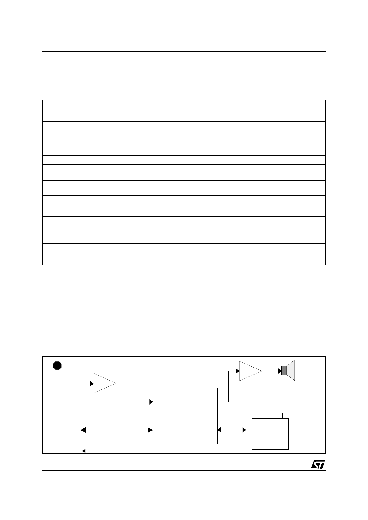
Figure 1.
8/12
audio amp
mic preamp
ADC DAC
TTDDAA7755550
µ
C
service request
slave I2C
0
EMI
FFLLAASSH
bbaannk
H
k
spkr
Up to
4 MB

TDA7550R - TDA7550 - TDA7551 - TDA7552 - TDA7553
TDA7551
SV208 Speaker Verification solution
The TDA7551 is a single-chip solution for speaker verification, featuring the Lernout & Hauspie SV208
verification engine. Pass-phrases can be stored by performing an enrollment (the pass-phrase must be
repeated three times), then the incoming prompt can be compared with the pre-stored pass-phrase to
verify the speaker identity.
Known password speaker recognition Noise-robust recognition of isolated words
Enrollment phase The speaker associates his identity to an utterance, which must last
Verification phase The claimed identity of the speaker is compared with the result of the
Control through I
Sample rate: 8 kHz
Equal error rate: > 94%
2
C Management of the verification engine is accomplished through an I2C
Figure 2.
from 1 to 2 seconds, and reapeat it three times; the algorithm performs
an analysis and accepts or rejects the enrollment phase.
verification phase, in which the input prompt is compared with the
selected pass-phrase.
protocol: the TDA7551 appears as a slave I
2
C device.
to extern al wo rld
Controller
mic preamp
ADC DAC
slave I2C
service request
TTDDAA7755551
audio amp
(optional )
spkr
1
EMI
FFLLAASSH
bbaannk
Pass- p hrases can reside here
Up to
H
4 MB
k
9/12

p
TDA7550R - TDA7550 - TDA7551 - TDA7552 - TDA7553
TDA7552
TTS3000 Text-To-Speech solution
The TDA7551 is part of a two-chip solution for Text-To-Speech, featuring the Lernout & Hauspie
TTS3000 engine. Two devices are needed:
A 16-bit microcontroller (ST10) for string analysis and conversion
•
The TDA7552 DSP for voice synthesis.
•
An external application sends ASCII strings to the microcontroller, which perform an analysis of the entire
sentence; language-dependent data is needed on the FLASH accessed by the ST10. As a result of the
analysis, a data stream is sent through I
DSP. The software running on the TDA7552 DSP is independent from languages.
2
C to the TDS7552 DSP. No external memory is required by the
Control through I2C Management of the DSP is accomplished through an I2C protocol: the
TDA7552 appears as a slave i
Many languages available The following languages are available:
US English, French, German, Italian, Spanish, Japanese. Other
languages available on request.
Sample rate: 11.025 kHz
Figure 3.
2
c device.
audio am
0
ASCII string
SSTT110
mmiiccrrooccoonnttrroolllleer
I2C
r
TTDDAA7755552
2
10/12
language-
dependent
code
bbaannk
H
k
FFLLAASSH
language-indep endent cod e

TDA7550R - TDA7550 - TDA7551 - TDA7552 - TDA7553
DIM.
mm inch
MIN. TYP. MAX. MIN. TYP. MAX.
A 1.60 0.063
A1 0.05 0.15 0.002 0.006
A2 1.35 1.40 1.45 0.053 0.055 0.057
B 0.22 0.32 0.38 0.009 0.013 0.015
C 0.09 0.20 0 .003 0.008
D 16.00 0.630
D1 14.00 0.551
D3 12.35 0.295
e 0.65 0.0256
E 16.00 0.630
E1 14.00 0.551
E3 12.35 0.486
L 0.45 0.60 0.75 0.018 0.024 0.030
L1 1.00 0.0393
K3.5°(min.), 7°(max.)
OUTLINE AND
MECHANICAL DATA
TQFP80
(14x14x1.40mm)
D
D1
D3
61
e
B
PIN 1
IDENTIFICATION
80
1
4160
40
E3
E1 E
Gage plane
0.25mm
21
20
K
TQFP80L
L
L1
0.10mm
Seating Plane
.004
A
A2
A1
C
11/12

TDA7550R - TDA7550 - TDA7551 - TDA7552 - TDA7553
Information furnished is believed to be accurate and reliable. However, STMicroelec tro nics assumes no responsibility for the consequences
of use of such informatio n nor for any infringement of patents or other ri ghts of third parties which may res ult from its use. No license is
granted by im plicat ion or ot herw ise under any patent or pat ent right s of ST Micro electronics . Speci fication ment ioned in this publication are
subject to c hange without notice. Thi s publication supersedes and replaces all informatio n previously supplied. STM i croelectronics products
are not authorized for use as critical components in life support devices or systems without express written approval of STMicroelectronics.
The ST logo is a registered trademark of STMicroelect roni cs
© 1999 STMicroelectronics – Printed in Italy – All Rights Reserved
STMicroelectronics GROUP OF COMPANIES
Australia - Brazil - China - Finland - France - Germany - Hong Kong - India - Italy - Japan - Malaysia - Malta - Morocco -
Singapore - Spain - Sweden - Switzerland - United Kingdom - U.S.A.
http://www.st.com
12/12
 Loading...