

DELTA/SIGMA CASCADE 20 BIT STEREO DAC
■ 20-bit resolution single ended output
■
Analog reconstruction third order Chebyshev filter
■ I2S input data format
■ On chip PLL
■ System clock: 64 Fs
■ 2 output channels
■ 0.9 VRMS single ended output dynamic
■ 3.3V power supply
■ Reset
■ Sampling rate 36KHz to 48KHz
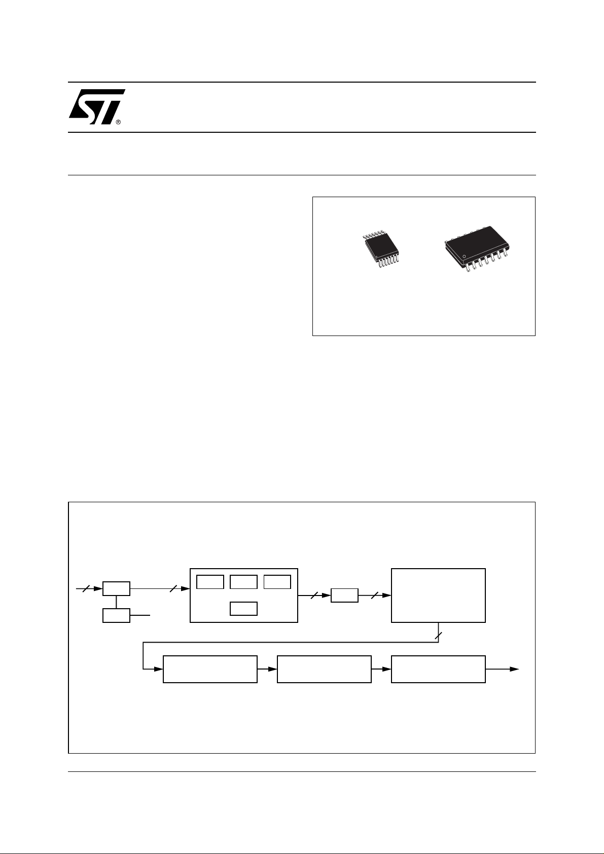
TDA7535
TSSOP-14 SO-14
ORDERING NUMBER: TDA7535
DESCRIPTION
The TDA7535 is a stereo, digital-to-analog converter
designed for audio application, including digital interpolation filter, a third order multi bit Delta-Sigma DAC,
a third order Chebyshev's reconstruction filter and a
differential to single ended output c onverter. This device is fabricated in highly advanced CMOS, where
high speed precision analog circuits are combined
with high density logic circuits. The TDA7535, according to standard audio converter s, can accept any
2
I
S data format.
BLOCK DIAGRAM
2
I
S
I2S
PLL
DIGITAL
INPUT
CLKOUT
20
F
FIR1 FIR2
S
ALU
FIR3
The TDA7535 is available in SO-14 and TSSOP-14
packages. The total power consumption is less than
75mW.
TDA7535 is suitabl e for a wi de variety of applicati ons
where high performance are required. Its low cost
and single 3.3V power supply make it ideal for several applications, such as CD players, MPEG audio,
MIDI applications, CD-ROM drives, CD-Interactive,
digital radio applications and so on. An evaluation
board is available to perform measurement and to
make listening tests.
20
8F
S
S&H
23
64F
Σ∆ MODULATOR
S
4
D02AU1417
July 2003
THERMO DECODER &
RANDOMIZER
3rd CHEBYSHEV
SC FILTER
DIFF TO SINGLE
CONVERTER
ANALOG
OUTPUT
1/9
TDA7535
ABSOLUTE MAXIMUM RATINGS
Symbol Parameter Value Unit
V
DD
V
CC
V
aio
V
dio
V
di5
T
T
stg
Warning: Oper ati on at o r be yo nd th ese li mit may r es ult i n pe rma nen t da mage to t he de vic e. N orm al opera tion is not g uaran te ed at th ese
THERMAL DATA
Symbol Parameter Value Unit
R
th j-amb
Note: 1. In still air
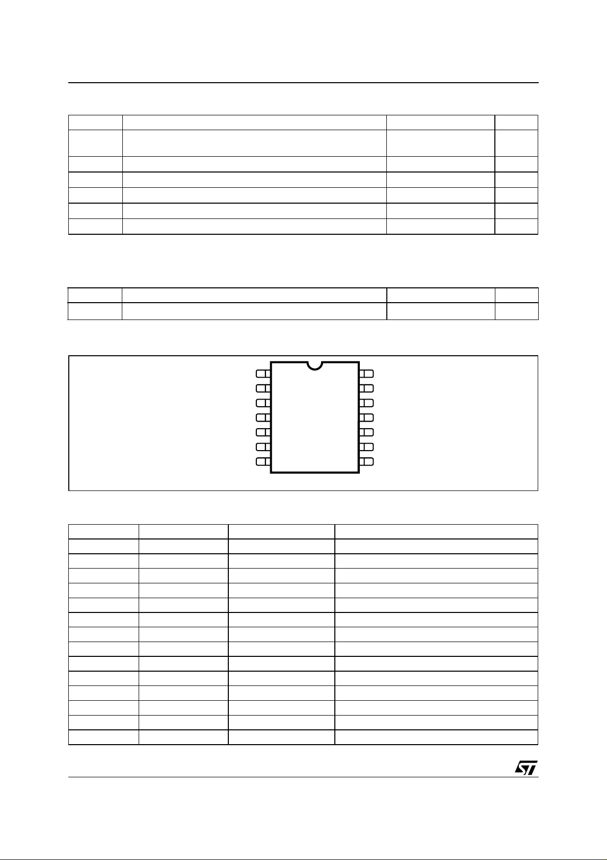
PIN CONNECTIONS (Top views)
Power supplies Digital
Analog
-0.5 to +4.6
-0.5 to +4.6
Analog Input and Output Voltage -0.5 to (VCC+0.5) V
Digital Input and Output Voltage -0.5 to (VDD+0.5) V
Digital Input Voltage (5V tolerant) -0.5 to 6.5 V
Operating Junction Temperature Range -40 to 125 °C
j
Storage Temperature -55 to 150 °C
extremes.
Thermal resistance junction to ambient
(1)
85 °C/W
V
V
N.C.
SDATA
SCK
N.C.
GND_DIG
GND_ANA
OUTSR
2
3
4
5
6
7
14
13
12
11
10
9
8
D01AU1276A
RESETN1
FSYNC
VDD_DIG
N.C.
VDD_ANA
VCM
OUTSL
PIN FUNCTION (SO14/TSSOP14)
Pin Number Pin Name Input/Output Power Description
1 N.C. - 2 SDATA I I2S Digital Data Input
3 SCK I I2S Clock Input
4 N.C. - 5 GND_DIG P Digital Ground
6 GND_ANA P Analog Ground
7 OUTSR O Right Channel single ended Output
8 OUTSL O Left Channel single ended Output
9 VCM P Reference 1.65V externally filtered
10 VDD_ANA P Analog 3.3V-Supply
11 N.C. - 12 VDD_DIG P Digital 3.3V-Supply
13 FSYNC I I2S Left-Right Channel selector
14 RESETN I Reset (active low)
2/9
TDA7535
RECOMMENDED DC OPERATING CONDITIONS
Symbol Parameter Test Condition Min. Typ. Max. Unit
V
3.3V Digital Power Supply
DD
Voltage
V
3.3V Analog Power Supply Voltage
CC
POWER CONSUMPTION
Symbol Parameter Test Condition Min. Typ. Max. Unit
I
Total Maximum Current
dd
power supply @ 3.3V and Tj = 125°C
GENERAL INTERFACE ELECTRICAL CHARACTERISTICS
Symbol Parameter Test Condition Min. Typ. Max. Unit
l
Low Level Input Current without
il
pullup device
High Level Input Current without
l
ih
pullup device
I
latchup
V
Note: 1. The leakage currents are generally very small, <1nA. The value given here, 1mA, is the maximum that can occur after an Electro-
I/O latch-up current V < 0V, V > V
Electrostatic Protection Leakage , 1µA (note 2) 2000 V
esd
static Stress on the pi n.
2. Human Body Model.
Vi = 0V (note 1) 1 µA
Vi = Vdd (note 1) 1 µA
dd
3.15 3.3 3.45 V
3.15 3.3 3.45 V
21.5 25 mA
200 mA
LOW VOLTAGE CMOS INTERFACE DC ELECTRICAL CHARACTERISTICS
Symbol Parameter Test Condition Min. Typ. Max. Unit
V
Low Level Input Voltage
il
V
V
High Level Input Volta ge
ih
Schmitt trigger hysteresis 0.8 V
hyst
0.8*V
dd
0.2*V
V
dd
V
DAC ELECTRICAL CHARACTERISTICS
Vdd = 3.3V; Tamb = 25°C; Input signal frequency = sinus wave generated by Audio Precision Sys.2; Input
Signal Amplitude = see notes; Noise Integration Bandwidth = 20Hz to 22KHz (A- weighted)
Parameter Test Condition Min. Typ. Max. Unit
Noise + Distortion
(see note 1)
Total Harmonic Distortion see note 2 94 dB
Dynamic range see note 3 96 dB
Crosstalk see note 4 -95 dB
Full Scale Output Voltage V
Input Sampling Rate 36 48 kHz
@0dB
@-6dBb
@-40dB
@-60dB
= 3.15 to 3.45V
dd
Full scale input
89
94
96
96
dB
dB
dB
dB
0.8 0.9 1.0 Vrms
3/9

TDA7535
DAC ELECTRICAL CHARACTERISTICS
(continued)
Vdd = 3.3V; Tamb = 25°C; Input signal frequency = sinus wave generated by Audio Precision Sys.2; Input
Signal Amplitude = see notes; Noise Integration Bandwidth = 20Hz to 22KHz (A- weighted)
Parameter Test Condition Min. Typ. Max. Unit
Passband Ripple 0.12 dB
Stopband @ 3dB
@ 90dB
44.1kHz Sampling Rate
Interchannel Gain Mismatch 0.05 0.1 dB
Note1: It is the ratio between the maximum input signal and the integration of the in-band noise after deducing the power of signal funda-
mental. It depends on the input signa l amplitude . In this case 0dB m eans full scale digital, 1kHz frequency used.
Note 2: It is the ratio of the rms value of the signal fundamental component at 0dB (full scale digital) to the rms value of all of th e harmonic
components in the band.
Note 3: measured using the SN R at -60dB input signal, with 60dB added to compensate for small inpu t s i gnal.
Note 4: Left channel on with 0d B/ 1kHz input signal, Ri ght channel on wi th DC input signal.
21.53
24.80
kHz
Figure 1. I2S interface Diagram
Left
Right
FSYNC
SCK
SDATA
MSB
32 * SCK
20 Bits
LSB
32 * SCK
20 Bits
MSB LSB
4/9

Figure 2. I2S Timings
TDA7535
t
sckr
Valid
Valid
t
sckf
SDATA
FSYNC
SCK
t
Timing D escri ption Minimum Maximum Unit
t
sck
t
sckpl
t
sckph
t
lrw-
t
lrw+
t
sds
t
sdh
t
sckr
t
sckf
(1)
SCK clock defines the Fs , being the Sa m pl e Rate. Thi s input clock n eeds a jitter below ~212ps
(2)
FSYNC switches inside the time window as specified w.r.t. to falling edge of SCK
Clock Cycle
SCK Phase Low
SCK Phase High
FSYNC switching time window before SCK falling edge
FSYNC switching time window after SCK falling edge
SDATA setup time 60 ns
SDATA hold time 30 ns
SCK rise time 1.5 ns
SCK fall time 1.5 ns
(1)
lrw-
t
lrw+
t
sckpl
t
sds
(2)
(2)
t
sdh
t
sck
t
sckph
1/(64*Fs) -
150ps
RMS
0.5*t
sck
0.5*t
sck
0 0.125*t
0 0.125*t
RMS
1/(64*Fs) +
150ps
- 1% 0.5*t
- 1% 0.5*t
RMS
+1% ns
sck
+1% ns
sck
-10 ns
sck
-10 ns
sck
ns
Figure 3. Power Up & Reset Sequence
V
DD
RESET
T
RES
T
RES Min 50ms
I2S bit clock (SCK) must be present 20ms before re set release to al l ow PLL locking.
D02AU1418
5/9

TDA7535
Figure 4. Frequency response
Figure 5.
2
S
I
C16
100nF
(*)
TP1
TP2
TP3
GND_DIG
GND_ANA
SDATA
SCK
FSYNC
VCM
C15
47µF 10V
(*)
+3.3 VDIG
R2 10K
U4
2
3
13
5
6
9
(*) AS CLOSE AS POSSIBLE TO THE PIN
C7
10µF
10V
14
SW1
RESETN
VDD_ANA
10
bead inductor
VDD_DIG
12
OUTSL
8
OUTSR
7
D02AU1419B
10µH
µP
+3.3VANA
100nF(*)
100nF(*)
TP5
TP6
TP7 J4
TP8
10µF
10µF
J3
BNC
OUTSL
BNC
OUTSR
6/9

TDA7535
DIM.
D (1) 8.55 8.75 0.336 0.344
F (1) 3.8 4 0.150 0.157
(1) D and F do not include mold flash or protrusions. Mold flash or
potrusions shall not exceed 0.15mm (.006inch).
MIN.. TYP. MAX.. MIN.. TYP.. MAX..
A 1.75 0.069
a1 0.1 0.25 0.004 0.009
a2 1.6 0.063
b 0.35 0.46 0.014 0.018
b1 0.19 0.25 0.007 0.010
C 0.5 0.020
c1 45˚ (typ.)
E 5.8 6.2 0.228 0.244
e 1.27 0.050
e3 7.62 0.300
G 4.6 5.3 0.181 0.209
L 0.4 1.27 0.016 0.050
M 0.68 0.027
S8˚
mm inch
(max.)
OUTLINE AND
MECHANICAL DATA
SO14
7/9

TDA7535
DIM.
mm inch
MIN. TYP. MAX. MIN. TYP. MAX.
A 1.200 0.047
A1 0.050 0.15 0 0.002 0.0 06
A2 0.800 1.000 1.050 0.031 0.039 0.041
b 0.190 0.300 0.007 0.012
c 0.090 0.200 0.005 0.009
D (1) 4.900 5.000 5.100 0.114 0.118 0.122
E 6.200 6.400 6.600 0.244 0.252 0.260
E1 (1) 4.300 4.400 4.500 0.170 0.173 0.177
e 0.650 0.026
L 0.450 0.600 0.750 0.018 0.024 0.030
L1 1.000 0.039
k 0˚ (min.) 8˚ (max.)
aaa 0.100 0.004
Note: 1. D and E1 does not include mold flash or protrusions.
Mold flash or potrusions shall not exceed 0.15mm
(.006inch) per side.
OUTLINE AND
MECH AN ICAL DAT A
TSSOP-14
(Body 4.4mm)
8/9
0080337 (Jedec MO-153-AA)

TDA7535
Information furnished is believed to be accurate and reliable. However, STMicroelectronics assumes no responsibility for the consequences
of use of such information nor for any infringement of patents or other rights of third parties which may result from its use. No license is granted
by implic ation or otherwise under any patent or patent r i ght s of STMi croelectr oni cs. Spec i fications mentioned i n this publication are subject
to change without notice. This publication supersedes and replaces all information previously supplied. STMicroelectronics product s are not
authorized for use as cri tical comp onents in lif e support devi ces or systems without express written approva l of STMicroel ectronics.
The ST logo is a registered trademark of STMicroelectronics
2003 STMicroelectronics - All Ri ghts Rese rved
Austra lia - Brazil - Canada - Chi na - F i nl and - Franc e - Germany - Hong Kong - In di a - Israel - Ita l y - J apan -Malaysia - Malta - Morocco -
Singap ore - Spain - Sw eden - Switze rl and - Unit ed K i ngdom - United States .
STMicroelectronics GROUP OF COMPANIES
http://www.s t. com
9/9
 Loading...