

Digital Servo & Decoder
■
BUILT IN 8Bit MICROCONTROLLER
(STANDARD ST7) with:
– 24 KByte ROM available for ST7 & Servo-Audio
DSP
– 1024Byte RAM, including 128byte stack
– 4KByte RAM for CD-Text memory (for 1block)
– Built in R-W subcode buffer (Max. 144Byte
8packs) for CD-Text
– 24 bit general I/O port (PoartA[7-0], PortB[7-0],
PortC[7-0])
– One External Interrupt (16 IRQ encoder inside)
– 16bit free running counter timer
– 8bit 1ch general purpose A/D
–I
2
C bus I/F
(14 x 14 x 1.40mm body)
– Watch dog
– Kenwood I/F
■
STAND-BY MODE (Stop all clocks and Shut down power of Peripheral (PON pin))
■
BUILT IN SERVO & AUDIO DIGITAL SIGNAL PROCESSOr (SAC-DSP) inclusive of:
– 1024x19bit Program RAM
– 512x16bit Coefficient RAM
– 1024x20bit Data RAM
– 128x6bit Decimation RAM
– MAC: 16 bit (Coefficients) x 20 bit (data) multiplier with 38 bit adder
– Instruction execution rate as high as 56MIPS
■
BUILT IN PROGRAMMABLE CLOCK GENERATOR PLL
■
PERIPHERALS for CD PLAYER APPLICATION
– Data Acquisition, Erasure correction, CLV&CAV controller
– Subcode decoder (CD-Text, CD-Graphic I/F)
– Shock proof memory controller, Disturbance detector
– Decimation filter
■
ACTUATORS DRIVING MODE SELECTABLE between PWM or PDM MODE
■
256Fs / 384Fs (16.9344MHz) CLOCK INPUT.
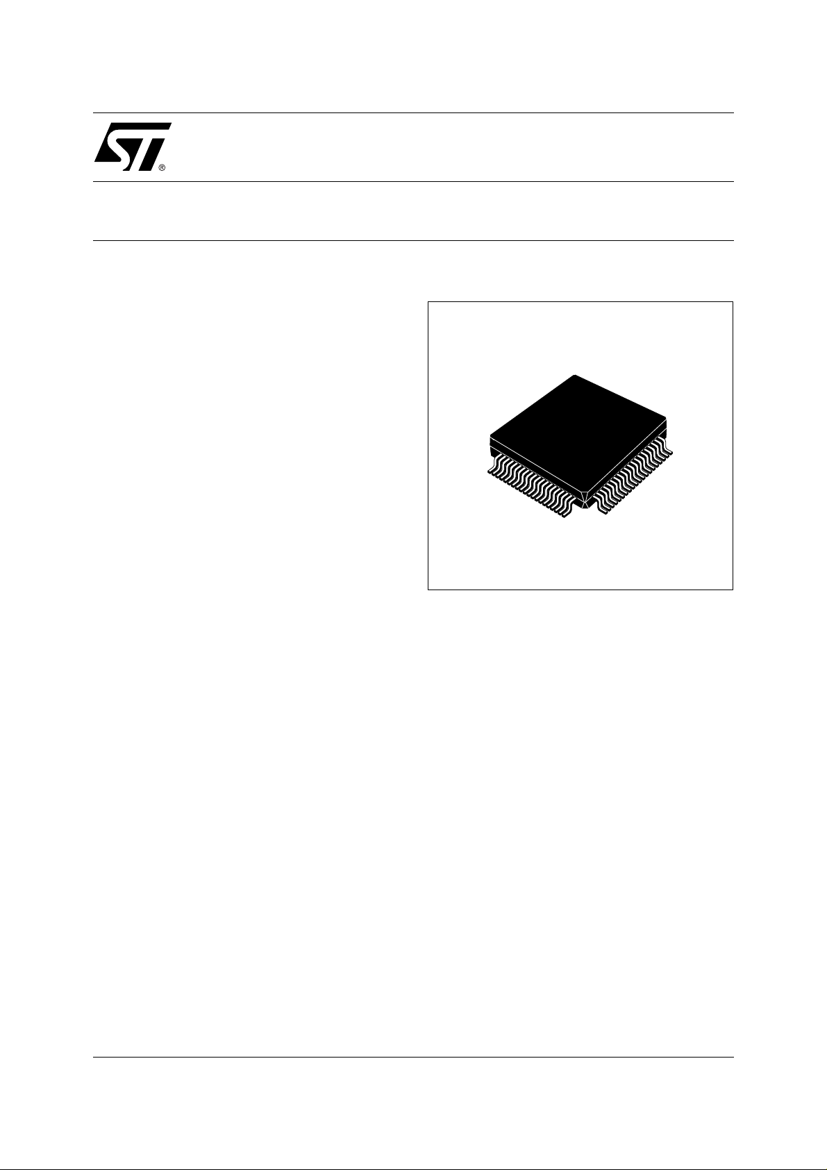
TQFP80
TDA7522
PRODUCT PREVIEW
May 1998
This is preliminary information on a new product now in development. Details are subject to change without notice.
1/23

TDA7522
1.0 DESCRIPTION
TDA7522
Audio. Main concept of this IC is that it is based on embedded System Micro Controller which allows customer to develop system software very easil y: just based on provided commands. Further the microcontroller is fully customer dedicated in terms of both software and general purpose Port.
By combination of ST Analog front-end IC (
Controller and CD-Text function can be realized.
The TDA7522 portfolio is constituted by three different versions:
– ’development’: which g ives the possibility to have a t disposal the complete sw develo pment environ-
ment, by means of a dedicated package
– ‘in field development’: standard package but with select ion o f program m em ory: on c hip RAM , on c hip
ROM. The program RAM is fully patchable through the stand ard IIC interface, giving the possibility of
sw changing while chip is working in the real environment.
– ‘production’: standard package, but with software permanently stored in the on chip ROM.
2.0 TECHNOLOGY
All version are produced using the HCMOS6 0.35um technology which works @3.3Vdc; to avoid interface
problem with existing logics, all digital Inputs are 5V tolerant. When interfacing logic on TDA7522 outputs,
user should take care of output levels that are at CMOS level @3.3V. Depending on output type the I
and Ioh value are guaranteed at 4mA or 8mA; the TDA7522 output driving specification will be included in
a next issue of this data sheet.
is a single chip processor consisting of Decoder, Servo and 1bit D/A for 4times CD-ROM / CD-
TDA7521
), all CD functions including Shock Proof Memory
ol
3.0 ADDITIONAL FEATURES
■
16Mbit DRAM I/F allows maximum 9 seconds shock proof
■
Built-in 1bit Delta Sigma modulation for DAC
■
Subcode P,Q and R-W decoding
■
Error Correction is capable of Dual C1 and quadruple C2 erasure corrections
■
Jitter absorbing capabilit y: +/- 6 frames
■
Automatic fine gain/balance/offset adjustme nt for tracking and focus servos
■
Built-in Digital Silence detection
■
Built-in EFM Demodulation/Sync Rear and Forward protection
■
Soft audio mute
■
Built-in Digital PLL with large capture range from 0.5 to 4 times speed
■
Digital Servo control for all servo loops
■
Capable of 2x and 4x speeds for shock proof and CD-ROM applications
■
Capable of wide temperature range (-40C to +85C) stable operation
■
Fast access times for CD-ROM applications due to wide Capture range and CAV mode run at max 4
times overspeed
■
CLV or CAV (lock-to-disk mode) spindle servo operations
■
Digital Output SPDIF (DIT CP340)
■
Sony LSI Output Interface (for Audio & CD-ROM)
■
Pulsate SLED mode support
■
Built in 8times Audio Over sampling filter.
2/23

Figure 1. Pin Connection
TDA7522 general ov erview is reported bel ow.
REMARK: CONSIDERING THE SELECTION DONE BY CUSTOMER, THE DRAM I/F COULD BE
SLIGTHY MODFIED. DETAILS WILL BE GIVEN IN A LATER ISSUE OF DATA SHEET.
TDA7522
PIN_SERDA 1
PIN_SERCK 2
PIN_DGTLIN0_OF 3
PIN_DGTLIN1_UF 4
PIN_DGTLIN2 5
PIN_DGTLIN3 6
PIN_DGTLIN4 7
PIN_DGTLIN5 8
PIN_DGTLIN_6 9
PIN_CORE_VDD_1 10
PIN_CORE_VSS_1 11
PIN_DGTLIN7 12
PIN_DGTSYNC 13
PIN_CLKOUT 14
PIN_BSR_SDK48 15
PIN_BSL_SAK48 16
PIN_LRCK 17
PIN_C2P0 18
PIN_MUTEL 19
PIN_MUTER 20
PIN_SFSR
PIN_KDMPHYS 21
PIN_DRD0
72
PIN_CORE_VDD_470
PIN_DRA175PIN_DRA274PIN_DRA373PIN_DRA4
PIN_CORE_VSS_471
PIN_DRA0
78
PIN_SPDL41PIN_TFSR42PIN_FFSR
77
PIN_DRD380PIN_DRD279PIN_DRD1
76
TDA7522
80-pin
26
25
PIN_XTI 24
PIN_PON 22
PIN_XTO
PIN_AVSS_1
PIN_AVDD_1 23
PIN_KADC_VRL 28
PIN_KADC_VRH 27
32
30
31
PIN_NRESET
PIN_KADC_IN 29
PIN_CORE_VSS_2
PIN_CORE_VDD_2
68
33
PIN_TESTEN
67
PIN_SCK 34
PIN_DRA569PIN_DRA6
PIN_DRA866PIN_DRA9
PIN_DRA7
64
63
62
65
PIN_SDA 35
PIN_SCANEN 36
61
60
59
58
57
56
55
54
53
52
49
48
47
46
45
44
43
PIN_KASEL 37
PIN_KTEST 38
PIN_MSTOP 40
PIN_KSEARCH 39
PIN_DRA10
PIN_DRA11
PIN_RAS
PIN_CAS
PIN_DWR
PIN_DRS
PIN_CLK
PIN_DATAM
PIN_DATAS
PIN_CORE_VSS_351
PIN_CORE_VDD_350
PIN_SRQ
PIN_CS
PIN_DOUT
PIN_SCOR
PIN_SBSO
PIN_EXCK
PIN_WFCK
PIN_K_VER_HOR
PIN_SLEDL
3/23

TDA7522
Table 1. Pin Description
Pin Number Name Function Description
01 SERDA I/O Data line for Serial I/F
02 SERCK O Clock line for Serial I/F
03 DGTLIN0_OF I HF bit 0 and Servo overflow
04 DGTLIN1_UF I HF bit 1 and Servo underflow
05 DGTLIN2 I HF bit 2 and Servo bit 0
06 DGTLIN3 I HF bit 3 and Servo bit 1
07 DGTLIN4 I HF bit 4 and Servo bit 2
08 DGTLIN5 I HF bit 5 and Servo bit 3
09 DGTLIN6 I HF bit 6 and Servo bit 4
10 CORE_VDD_1 Vdd Digital Power supply
11 CORE_VSS_1 Gnd Digital Ground
12 DGTLIN7 I HF bit 7 and Servo bit 5
13 DGTSYNC I Sync strobe for Multiplexer
14 CLKOUT O System clock output to TDA7521
15 BSR_SDK48 O LSI I/F clock output or
DAC bit stream right channel output
16 BSL_SAK48 O LSI I/F data output or DAC bit stream left channel output
17 LRCK O LSI I/F L/R signal
18 C2PO O Validity flag output for CD-ROM decoder
19 MUTEL O Mute left signal (active high)
20 MUTER O Mute right signal (Active high)
21 KDMPHYS I/O De-emphasis indication or ST7 GPIO PA2
22 PON I/O System shutdown pin for power saving mode or
23 AVDD_1 Vdd Analog power supply
24 XTI I Crystal input
25 AVSS_1 Gnd Analog ground
26 XTO O Crystal output
27 KADC_VRH I ADC top reference Voltage input
28 KADC_VRL I ADC bottom reference Voltage input
ST7 GPIO PC7
29 KADC_IN I ADC input
30 CORE_VDD_2 Vdd Digital Power supply
31 CORE_VSS_2 Gnd Digital Ground
32 Nreset I Hardware reset
4/23
Pin Number Name Function Description
33 TESTEN I Test enable signal (Active low)
34 SCK I IIC I/F clock signal
35 SDA I/O IIC I/F data
36 SCANEN I Scan enable (active high) or select DRAM outputs as TEST
outputs when TESTEN is inactive
37 KASEL I/O DAC polarity selection pin or ST7 GPIO PA0
38 KTEST I/O User test mode selection or ST7 GPIO PA1
39 KSEARCH I/O Gain change during search or ST7 GPIO PA3
40 MSTOP I/O interrupt request/stand-by pin or ST7 GPIO PC5
41 SLEDL I/O SLED limit switch or ST7 GPIO PC6
42 K_VER_HOR I/O Indication of vertical or horizontal operation
or ST7 GPIO PA4
43 WFCK O Write Frame clock for Subcode P-W output
44 EXCK I SBSO readout clock input
TDA7522
45 SBSO O Subcode P-W serial output
46 SCOR O Subcode sync output
47 DOUT O SPDIF Digital audio output
48 CS I/O ST7 GPIO PC4
49 SRQ I/O ST7 GPIO PC3
50 CORE_VDD_3 Vdd Digital Power supply
51 CORE_VSS_3 Gnd Digital Ground
52 DATAS I/O ST7 GPIO PC2
53 DATAM I/O ST7 GPIO PC1
54 CLK I/O ST7 GPIO PC0
55 DRS I/O Shock proof memory Read control
56 DWR I/O Shock proof memory Write control
57 CAS I/O Shock proof memory Column address select
58 RAS I/O Shock proof memory Row address select
59 DRA11 I/O DRAM Address 11
60 DRA10 I/O DRAM Address 10
61 DRA9 I/O DRAM Address 9 or Mirror signal output
62 DRA8 I/O DRAM Address 8 or TZC (Tracking Zero Cross) signal output
63 DRA7 I/O DRAM Address 7 or FOK (Focus OK) signal output
64 DRA6 I/O DRAM Address 6 or ST7 GPIO PB7 or PLLINF signal output
5/23
TDA7522
Pin Number Name Function Description
65 DRA5 I/O DRAM Address 5 or ST7 GPIO PB6 or OFS (FIFO Overflow) signal
output
66 DRA4 I/O DRAM Address 4 or ST7 GPIO PB5 or WFCK (Write Frame Clock)
signal output
67 DRA3 I/O DRAM Address 3 or ST7 GPIO PB4 or RFCK (Read Frame Clock)
signal output
68 DRA2 I/O DRAM Address 2 or ST7 GPIO PB3
69 DRA1 I/O DRAM Address 1 or ST7 GPIO PB2
70 CORE_VDD_4 Vdd Digital Power supply
71 CORE_GND_4 Gnd Digital Ground
72 DRA0 I/O DRAM Address 0 or ST7 GPIO PB1
73 DRD0 I/O DRAM Data 0 or ST7 GPIO PA5
74 DRD1 I/O DRAM Data 1 or ST7 GPIO PA6
75 DRD2 I/O DRAM Data 2 or ST7 GPIO PA7
76 DRD3 I/O DRAM Data 3 or ST7 GPIO PB0
77 SPDL O PWM/PDM Spindle motor control signal output
78 TFSR O PWM/PDM Tracking actuator control signal output
79 FFSR O PWM/PDM Focusing actuator control signal output
80 SFSR O PWM/PDM SLED motor control signal output
Note: 1. Depending from new DRAM sel ection pin nr.59 could be not used in prod uction versi on.
6/23
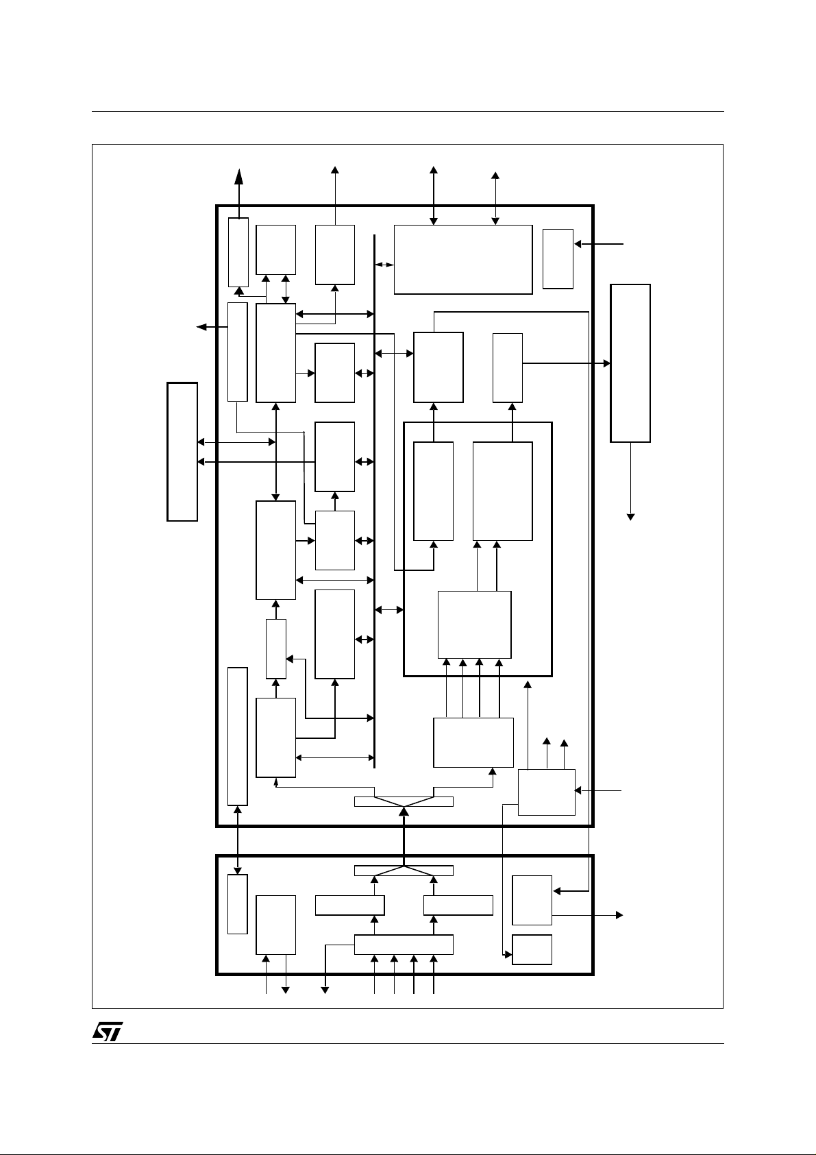
Figure 2. Block Diagram
TDA7522
CD TEXT Graphical
4M / 16M bit DRAM
Interface
TE
GPIO
I2C I/F
PDM / PWM
Track Loop filter
Focus Loop filter
SLED Loop filter
FE
ADC
ADC In
4ch Driver IC
ex. TDA7 473
Focus Actuator
Track Actuator
Sled Motor
Spindle Motor
Digital
SPDIF
CLV/CAV
Shock proof
Memory
Subcode
out
controller
controller
decoder
Out
LSI Digital
16Kbit
Cross Inter l eaving
Digital PLL &
Sync protection &
RAM
Reed-Solomon
EFM demodulator
LSI I/F
CD Text Extractor
I2C
bus
ST7
24KB ROM
1kbyte RAM
Delta
Sigma
Modulation
8x Audio OVS
Audio Processing
TDA7522(80pins)
TDA7521(44pins)
TDA7521 I/F Contro l
MPU I/F
Digital
Laser
AC
Servo
Adjustment
F
E
BD
Down
sampling
filter
Clock
ADC
1bit DAC
ST7 Clock
Peripherals Clock
DSP Clcok
PLL
Analog
+ filter
PLL
External Qu ar tz
AUDIO out
Slicer
Equalization
control
HF
Disturbance
(Mirror) detector
HFACBDEF
HF
ADC
A+C
DSP
Amp
E
F
B+D
7/23

TDA7522
Table 2. Main DC Characteristics (I)
Current input Condition Min Typ Max Unit
A+C diode input 1 16 µA
B+D diode input 1 16 µA
E diode input 1 16 µA
F diode input 1 16 µA
Table 3. Main DC Characteristics (II)
Voltage input Condition Min Typ Max Unit
A+C diode input 45 700 mVpp
B+D diode input 45 700 mVpp
E diode input 45 700 mVpp
F diode input 45 700 mVpp
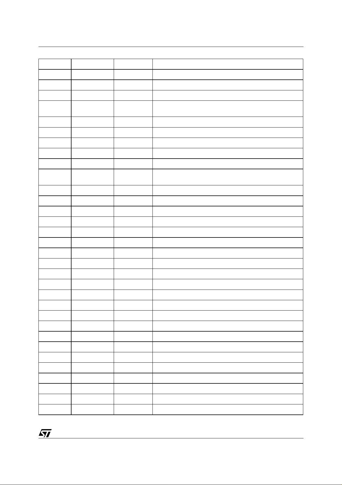
4.0 STANDARD VERSION MEMORY MAP
The memory spase, as seen by ST7 is defined in table 4; please take note that there are registers which
are used for less than 8 bit or, on the other side, when read only certan bit contain useful information. Referr to appendix a to have a complete list of register structure.
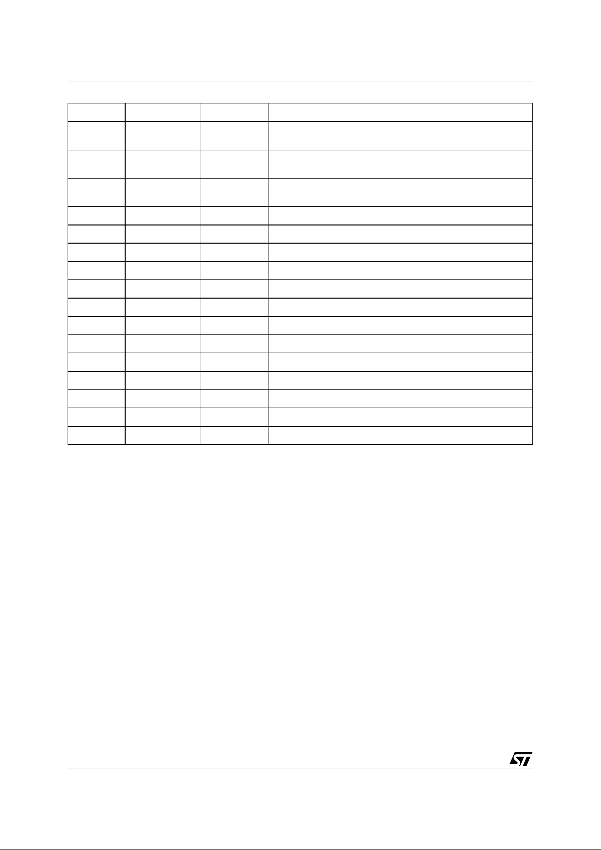
Table 4. TDA7522 Memory Map
Address Block Register name
0000h
0001h
0002h
0003h
0004h
0005h
0006h
0007h
0008h
........
000Bh
000Ch ST7 Miscellaneous Register 00h See specifications
000Dh Not Available
000Eh
000Fh
0010h
Port A
Port B
Data Register
Data Direction Register
Option Register
Pull Up Register
Data Register
Data Direction Register
Option Register
Pull Up Register
Reserved
Reserved for ST7 TEST
Reset
Status
00h
00h
00h
00h
00h
00h
00h
00h
Remarks
R/W Register
R/W Register
R/W Register
R/W Register
R/W Register
R/W Register
R/W Register
R/W Register
8/23

TDA7522
Address Block Register name
0011h
0012h
0013h
0014h
0015h
0016h
0017h
0018h
0019h
001Ah
001Bh
001Ch
001Dh
001Eh
001Fh
0020h
0021h
0022h
0023h
Timer
Port C
Control Register 2
Control Register 1
Status Register
Input Capture 1 High Register
Input Capture 1 Low register
Output Compare 1 High register
Output Compare 1 Low Register
Counter High Register
Counter Low Register
Alternate Counter High Register
Alternate Counter Low Register
Input Capture 2 High Register
Input Capture 2 Low register
Output Compare 2High register
Output Compare 2Low Register
Data Register
Data Direction Register
Option Register
Pull Up Register
Reset
Status
00h
00h
00h
00h
00h
00h
00h
FFh
FCh
00h
00h
00h
00h
00h
00h
00h
00h
00h
00h
Remarks
R/W Register
R/W Register
Read only
Register
Read only
Register
Read only
Register
R/W Register
R/W Register
Read only
Register
Read only
Register
Read only
Register
Read only
Register
Read only
Register
Read only
Register
R/W Register
R/W Register
R/W Register
R/W Register
R/W Register
R/W Register
0024h WD Watch Dog Configuration Register 7Fh R/W Register
0025h Not Available
0026h
0027h
0028h
0029h
002Ah
002Bh
002Ch
002Dh
002Eh
002Fh
0030h
0031h
0032h
0033h
0034h
0035h
0036h
0037h
0038h
0039h
003Ah
2
C
I
Equalizer
Subcode
Extraction
CR: Control Register
SR1: Status Register 1
SR2: Status Register 2
Not Used (CCR: Clock Control Register)
OAR1: Own Address Register 1
TX_DATA: Transmission Data
RX_DATA: Received Data
EQU_HPF: Controll & HP Filter Coefficient
EQU_FIR0: FIR Filter Coefficient
EQU_FIR1: FIR Filter Coefficient
EQU_FIR2: FIR Filter Coefficient
EQU_FIR3: FIR Filter Coefficient
EQU_FIR4: FIR Filter Coefficient
EQU_FIR5: Gain Register
QSR: Q Subcode Status Register
QSD: Q Subcode Data Register
CDTSR: CD Text Status Register
CDTDR: CD Text Data Register
00h
00h
00h
00h
00h
00h
00h
00h
00h
00h
00h
00h
00h
00h
00h
00h
00h
00h
R/W Register
Read only
Register
Read only
Register
R/W Register
R/W Register
R/W Register
R/W Register
R/W Register
R/W Register
R/W Register
R/W Register
R/W Register
R/W Register
R/W Register
R/W Register
R/W Register
R/W Register
R/W Register
Not Available
Not Available
Not Available
9/23

TDA7522
Address Block Register name
003Bh
003Ch
003Dh
003Eh
003Fh
0040h
0041h
0042h
0043h
0044h
0045h
0046h
0047h
0048h
0049h
004Ah
004Bh
004Ch
004Dh
004Eh
004Fh
Shock Proof
(HSY)
Bit Detection
and Clock
Recovery
WP1: Preset of Write Pointer Lower
WP2: Preset of Write Pointer Upper
CSR: Control/Status Register
WA1: Latest Stored valid Audio Frame Lower
WA2: Latest Stored valid Audio Frame Upper
RL1: Ram Level Lower
RL2: Ram Level Upper
DRR: Dummy Read to reset W/R Counter
PHIGAIN: Phase Gain
FRQCFG: Frequency Loop Configuration
FRQGAIN: Frequency Loop Gain
FRQ_L: Present Loop Output Freq Lower
FRQ_U: Present Loop Output Freq Upper
FRQI_L: Initial Loop Output Freq Lower
FRQI_U: Initial Loop Output Freq Upper
BD_INTEN: Interrupt Enable
BD_INTSRC: Interrupt Source Register
PHICFG: Configuration for Phase Loop
PLLGAIN: LP Filter Coefficients for ADPLL
PLL_SETUP: Overall control/co nfigurat ion
PLL_STATUS: PLL mode Status Flag
Reset
Status
00h
00h
00h
00h
00h
00h
00h
00h
00h
00h
00h
00h
00h
00h
00h
00h
00h
00h
00h
00h
00h
Remarks
R/W Register
R/W Register
R/W Register
Read only
Register
Read only
Register
Read only
Register
Read only
Register
Read only
Register
R/W Register
R/W Register
R/W Register
R Register
R Register
R/W Register
R/W Register
R/W Register
R/W Register
R/W Register
R/W Register
R/W Register
R Register
0050h
0051h
0052h
0053h
0054h
0055h
0056h
0057h
0058h
0059h
005Ah
005Bh
005Ch
005Dh
005Eh
005Fh
0060h
0061h
0062h
0063h
0064h
0065h
0066h
0067h
Event
Detection
SERVO
SPDIF
Interface
SETUP: Overall control/configurat ion
STATUS: Status Flag
RAMP: Peak detector decoding rate
DROPTHR: Dropout Threshold
DROPTIM: Dropout Timeout
FOCTHR: Focus Thres. Quality
MIRRPARS: Parameters for mirror signal
MIRRTHR: Thr for mirror env. for trk search
MIRRHYS: Hysteresis for MIRRTHR
TRK_CNTL: Tracking Counter Lower
TRK_CNTU:Tracking Counter Upper
ED_INTEN: Interrupt Enable
ED_INTSRC: Interrupt Source Register
SV_Servo_CR: Servo Control Register
SV_TWC_CR: Tracking Window Comparator CR
SV_TWC_CSR: TWC Control/Status Register
FS_CR: Focus Search Control Register
CRSR: Status Register
CSLO: Left Channel, LSBs
CSL1: Left Channedl, MSBs
CSR0: Right Channel, LSBs
CSR1: Right Channel, MSBs
00h
00h
00h
00h
00h
00h
00h
00h
00h
00h
00h
00h
00h
00h
00h
00h
00h
00h
00h
00h
00h
00h
R/W Register
R Register
R/W Register
R/W Register
R/W Register
R/W Register
R/W Register
R/W Register
R/W Register
R/W Register
R/W Register
R/W Register
R/W Register
R/W Register
R/W Register
R/W Register
R/W Register
Not Available
R/W Register
R/W Register
R/W Register
R/W Register
R/W Register
10/23

TDA7522
Address Block Register name
0068h
0069h
006Ah
006Bh
006Ch Not Available
006Dh
006Eh
006Fh
0070h
0071h
0072h
0073h
0074h Not Available
0075h
0076h
0077h
0078h
0079h
007Ah
007Bh
007Ch
007Dh
007Eh
PWM
/PDM
PLL PLL_CR1: Control Register 1
CLV/CAV CLV_CR1: Control Register 1
Decimation DEC_SR: Decimation Status Register
KIF
Interface
Interrupt
MASK
CIRC
SLED_CR: Sled Control Register
SLED_DR: Data to control the sled by ST7
SPDL_DR: Data to control spindle motor
PWM_CR: Pwm output control register,
CLKCNTL: Clock Control Register
CLV_CR2: Control Register 2
CLV_CR3: Control Register 3
DEC_CR: Decimation Control Register
KENWOOD I/F: Register 1
KENWOOD I/F: Register 2
MASK1: Interrupt Mask Enable Register
MASK2: Interrupt Mask Enable Register
CONFIG1: Configuration register for CIRC
CONFIG2: Configuration register for CIRC
FIFO1: Offset between read & write pointer
FIFO2: Status register for FIFO
C1ERRS: Error number by C1 decoder
C2ERRS: Error number by C2 decoder
Reset
Status
00h
00h
00h
00h
40h
00h
05h
00h
40h
00h
00h
00h
00h
00h
00h
1Ah
19h
C0h
00h
00h
00h
Remarks
R/W Register
R/W Register
R/W Register
R/W Register
R/W Register
R/W Register
R/W Register
R/W Register
R/W Register
R Register
R/W Register
R/W Register
R/W Register
R /W Register
R/W Register
R/W Register
R/W Register
R Register
R/W Register
R/W Register
R/W Register
007Fh DAC DAC_CSR: Control /Status Register 00h R/W Register
0080h
0081h
0082h
0083h
0084h
0085h
0086h
0087h
0088h
0089h
008Ah
008Bh
008Ch
008Dh
008Eh
008Fh
0090h
0091h
0092h
0093h
0094h
SAC_DSP
CXD
(Crossover
Detection)
TEST
SELECTION
DATA_LB: Lower Byte Data Register
DATA_MB: Middle Byte Data Register
DATA_UP: Upper Nibble Data + service bit
DATA_AR_LB: Data Address
COEF_AR_LB: Coefficient Address
PROG_AR_LB: Program Address
DCPSR: Miscellaneous Control/Data Reg.
DSP_ALU1: ALU contains, LSBs
DSP_ALU2: ALU contains, MSBs
AUDIOC: Audio Control Register
DSP_CR: Control Register
SHOCK_CMP: Shock Comparor
G1-EQUALISER: Coefficient Value
G2-EQUALISER: Coefficient Value
G3-EQUALISER: Coefficient Value
MUX_1: used only on development version
MUX_2: used only on development version
00h
00h
00h
00h
00h
00h
00h
00h
00h
00h
00h
00h
00h
00h
00h
R/W Register
R/W Register
R/W Register
R/W Register
R/W Register
R/W Register
R/W Register
R Register
R Register
R/W Register
R/W Register
R/W Register
Not Available
Not Available
Not Available
Not Available
R/W Register
R/W Register
R/W Register
R/W Register
R/W Register
11/23

TDA7522
Address Block Register name
0095h
0096h
0097h
0098h
0099h
009Ah
009Bh
009Ch
009Dh
009Eh
009Fh
00A0h
to
049Fh
04A0h to
8FFFh
9000h to
9FFFh
A000h to
FFDFh
ADC
TEMP.
UART TDA7521 I/F: Data Register
ADC_CR:Control Register
ADC_DATA: ADC Readout Value
TDA7521 I/F: Controll Register
4KBytes of CDTEXT RAM
RAM 1024Bytes
including
(STACK 128Byte)
Not Available
ROM 24KBytes
Reset
Status
00h
00h
Remarks
Not Available
Not Available
Not Available
Not Available
Not Available
Not Available
Not Available
R/W Register
R/W Register
FFE0h to
FFFFh
User Vectors Interrupt and Reset Vectors
4.1 ST7 Scratch Memory Ma p
As far as concern ST7 scratch memory, it is mapped as follow:
00A0 - 00FF RAM
0100 - 017F Stack
0180 - 049F RAM
total is 1024 Kbyte.
12/23

4.2 ST7 Interrupts Reg is te rs Conf i guration & Jum p Table
The TDA7522 peripheral interrupt vector is as follows:
-Register MASK1[7:0]:
bit positi on Des c ri ptio n Interrup t Nam e
MASK1[7] NO T USED
MASK1[6] NOT USED
MASK1[5] SUB_IRQ_Q Subcode extraction channel Q
MASK1[4] SUB_IRQ_RW Subcode extraction channel RW
MASK1[3] SP_OVER Shock Proof
MASK1[2] I2C_INT IIC
MASK1[1] PLL_i nt Analog Plll
MASK1[0] DSP_shock SAC-DSP
register MASK2[7:0]
bit positi on Des c ri ptio n Interrup t Nam e
MASK2[7] NOT USED
MASK2[6] NOT USED
MASK2[5] HSY_ int Digital PL L
MASK2[4] EVD_int Event detector
MASK2[3] CIRC_over Cross Interleave RS Code
MASK2[2] reserved
MASK2[1] reserved
MASK2[0] KIF_IRQ Kenwood interface.
TDA7522
Interrupts vector is reported below:
Interrupt Vector Jump Address Source Event Source Peripheral
ITCPU11 : ffe6 CIR_over CIRC
ITCPU10 : ffe8 E VD _int Event Detector
ITCPU9 : ffea HSY_int HFSync
ITCPU8 : ffec DSP_shock SAC-DSP
ITCPU7 : ffee P LL_i nt Ana log PLL
ITCPU6 : fff0 I2C_int I2C
ITCPU5 : fff2 SP_over Shock Proof
ITCPU4 : fff4 SUB_IRQ_RW Subcode/Contro l Extraction
ITCPU3 : fff6 SUB_IRQ_Q Subcode/Control Extraction
ITCPU2: fff8 TIMERINT TIMER interrupt
ITCPU1 : fffa OEXTIT PORT C interrupt
TRAP : fffc OTRAPIT software interrupt
RESET : fffe OSTART external reset.
13/23

TDA7522
Interrupt management it is fairly flexible, in det ail, when an i nterrupt i s s erved t he I flag of t he ST 7 i s automatically set (that means no other interrupts are served) and it is reset again only when the routine ends.
No interrupts can be missed because of the internal software-based acknowledgement scheme for peripherals. In order to reset an interrupt coming from a peripheral you have to write to '0' a relevant flag inside
it. With the TDA7522 interrupt mask register y ou just prev ent t he int errupt s ignal f rom c oming t o the ITC
(interrupt controller) and so you can change the priority without losing any interrupt.
4.3 Development Version Memory Configuration
For system application development a dedicated version will be available: the development version gives
the possibility of:
– use the ST7 emulator, for sw debug purpose;
– use of program RAM or ROM for sw execution and modification.
See appendix B for detail about memory map and TDA7522 operating modalities as:
– TDA7522 booting through I2C
– TDA7522 booting from PROM
– TDA7522 booting from PRAM.
When RAM is selected, all appli cation s w shal l be loade d through I2C, usin g the f acility as giv es by the
boot ROM.
When RAM configuration is selected, memory addresses are just overlapping the ROM defined in memory
map reported in appendix B.
TDA7522 development version can work also with emulator; refer to appendix B about the way to enter in
“ST7 emulation” mode.
NOTICE: due to different environment the following registers can be different between various versions:
– IIC register 27h: boot bit will disappear in production version
– KIF registers 75h and 76h are not available on development version
– Mux Registers 93h and 94h will both be available on production version.
5.0 FUNCTION DESCRIPTION
5.1 ST7
ST7 is based around an industry standard 8 bit core and offers an enhanced instruction set. The processor
runs with 8MHz internal clock. Due to fully static design of this device, operation down to DC is possible.
Under software control the ST7 can be placed in Wait or Halt mode for reducing power consumption. ST7
can switch off crystal clock to disable complete functions of IC as well.
The enhanced instruction set and addressing modes afford real programming potential; in addition to standard 8 bit data management the ST7 features true bit manipulation, 8x8 unsigned multiplication and indirect addressing modes. The device includes a CPU, ROM, RAM, I/O, General I/O Port, 16 interrupt
encoder, timer.
14/23

Figure 3. ST7 Interface Overview
(
)
)
y
y
g
)
)
TDA7522
Peripher al 1Peripheral 2Peripheral n
Gene ral Purpose I/O
CS
1024
Bytes
RAM
Port A,B
CS
TIMER Watchdo
IMU AGU
ST7 CORE
CS
CS
Address Bus (0:15
Data Bus (0:7
CD TEXT
4 KB
tes
RAM
CS
Address Bus
Data Bus (0:7
CS
24 KB
ROM
0:6
tes
TDA7522
PERIPHERALS
ST7 is Supervisor of complete CD system such as Servo, Main Processor Communication, DSP control.
Some Tasks of ST7 are as follows:
– Supervisor of all sub blocks
– Initialization of Coefficients for SAC-DSP Digital Servo
– Initialization of parameters of all sub blocks
– Focus search and quick restart
– Coarse Adjustments for Gain(Laser), Offset in Analog front end
– Fine Adjustments for Balance, Offset, Servo Gain in DSP
– Command interpreter and communication with external MPU
– Play & Subcode control, Music search, Random search, Program Play, Scan, Repeat etc.
– One, Ten and Long tracking jump and Pause implementa tion
– Linear velocity measurement (disc speed)
– Computation of the number of tracks for jum p
– Shock proof memory control for data synchronization after shock
15/23

TDA7522
– Constant Angular Velocity Control
– TOC management
– CD-Text I/F.
5.2 DSP (SACDSP : Serv o Aud io Control Digit a l Signal Processor)
DSP is placed as a subset of ST7 MPU, which performs Digital Filter calculation.
It consists of 20bit (data) x 16bit (coefficient) multiplier, 38bit accumulator, 20bit Data RAM, Data Arbitra-
tion between ST7, and 19 bits wide program Opcode; it can be broken down into two instruction bindings:
– Inst ruction binding #1 :Arithmetic Instructions + Parallel Move Instructions
– Inst ruction binding #2 :Immediate moves and bit-test jumps
SACDSP is very powerful DSP which performs more than 50MIPS, and it is based on three level pipeline
architecture in which concurrent instruction fetch, decode, and execution occur.
Figure 4. Basic I/Fs to ST7
Scratch RAM
Coeff.
RAM
Decimation
filter
Coeff.
Arbitration
PRAM
Loaded
by ST7
ST7 & Peripherals
SAC-DSP
PROM
Data
Arbitration
PDM/PWM
SERVO DATA Path
Data
RAM
CIRC
AUDIO DATA Path
Audio
DAC
Some Tasks of SACDSP are as follows;
– DSP: Digital Filter execution as slave of ST7
– Focusing and Tracking loop filter
– Sled Tracking control
– Pick-up Velocity control during Jump
16/23

TDA7522
– Some Digital filters for Adjustments by ST7
– Sine wave generator for reference of internal adjustment and DAC measurement
– Filter for Shock detector
– 8 times high end Audio Over sampling
– De-emphasis filter
– Audio attenuation, mute and balance
– Internal Signal observation feature for user measurement
– Soft mute and data concealment
– Audio peak detection
– Focus error, Tracking error generation
– Equalization of Tracking Zero Cross signal
– Sound Vector Enhancement filter.
5.3 DATA Acquisition
The digital HF signal is input to an digital equalizer to improved the bit detection. Different equalizer coefficients are selectable by MPU.
The digital data slicer is implemented and the internal slice level is calculated by using a leakage free integrator which is subtracted from HF. The properly levelled EFM is delivered to the edge detector and a
digital bit clock PLL. On this stage, no analog VCO is necessary to obtain bit c lock but DTO (Discrete Time
Oscillator) is used.
The Digital PLL block consists of following functions;
– Adaptive HF Equalization
– HF HPF for disturbance rejection
– Digital Dat a s lic er
– Linear interpolation for Phase error measurement
– Run length detection for Frequency error measurement
– Frequency & Phase Control loop
–DTO block
– EFM bit generation.
The serial bit stream signal from the phase detected is sent to a shift register block, which includes differ-
ent functions as follows;
– serial to parallel conversion
– detection of frame sync pattern
– protection and insertion of frame sync
– bit clock counter (588 bits per frame)
– synchronization and sync window logic
– 14 to 8 bit demodulation
– subcode extraction.
5.4 Subcode extraction
This block receives the subcode data stream and the related S0/S1 synchronization information from Acquisition part.
17/23

TDA7522
Subcode processing consists of CRC parity check and Subcode decoder.
There are 2 different buffers for Q Subcode data and for R-W subcode data.
Q subcode data is transferred to ST7 every symbol by interruption and the result of CRC is also reported
to ST7. R-W subcode data es pecially for CD-Text data t hrough program area is arranged to 8bit format
from 6bit of R to W, then ST7 stores max. 144byte (8pack data) as a FIFO to allow the tolerant of reading
timing from external MPU for display and also 1block CD-Text data from TOC area can be transferred to
ST7 4Kbyte CD-Text RAM.
5.5 CIRC (Error correction)
CIRC (Cross Interleaving Read Solomon code) consists of 2 following blocks;
– Memory control for
M1: The FIFO memory to absorb Jitter of input signals
M2: The De-interleaving memory
M1 FIFO memory com pensat es th e speed deviations of the spindle m oto r and M 2 is used for the de-interleaving between the C1 and C2 decoder. The size of the RAM is 16Kbit and the width is 9bit. Each 9
bit word consists of 8 bit data (symbols) and 1 bit validity flag.
– Error Correction
This block represents a Reed Solomon decoder which forms a CIRC decoder for CD in conjunction with
CIRC RAM.
There are two decoder circuits:
– the first C1 decoder can correct up two random errors in a 32-byte frame, marking uncorrectable errors
as erasures
– the second C2 decoder can correct up to four erasures in a 28 byte frame.
5.6 Shock pro of m em ory control
This is a shock proof memory controller which absorbs the interruption due to the shocks.
Namely, it controls external DRAM in order to store the audio data into RAM earlier than the reading.
Therefore during shocks the data of the RAM can be played without any interruption of the data.
The controller handles the data from Acquisition and out put into RA M&Ti ming block . It mea ns the st ored
data into RAM is ADAT[7-0] bef ore error correc tion. Tha t is why com plete 32 Symbols / Frame includ ing
CRC must be stored into RAM. It allows the use of Audio RAM (ARAM) with defects which is much cheaper than standard DRAM.
The difference between the classical shock proof memory controller like SONY and this new controller is
that ARAM use with def ects, the location of the mem ory and the controller, and also h ow to fill the dat a
into RAM earlier than reading. In case of our controller, CLV servo (Disk motor controller) varies the disk
speed in order to store certain amount of data into RAM earlier than the reading. Then as long as certain
amount of data is k ept in the RAM in a dvance, the disk speed is controlled with single speed (normal
speed) operation, not always double speed operation like classical solution.
Mainly the shock proof memory controller consists of 3 controllers.
One is the writing pointer controller which controls the memory address for writing data, the another is the
reading pointer controller which controls the memory address for reading data, the other is timing arbitration between the reading and writing procedure of the data and address.
The output data fro m the m em ory is deli vered al ways with fixe d da ta rate wi thou t jitters, h owev er the incoming data is not delivered with fixed rate because of the jitters from the disk and the varied speed of the
18/23

TDA7522
disk motor, so the data rate changes within the capture range of the digital PLL in the Acquisition part. So
output data has no jitters that M1 buffer me mory in RAM&Timing can be rep laced with the shock proof
memory. (as a huge time base collector instead of M1 buffer memory).
5.7 CLV & CAV
This is a spindle motor (Disc motor) servo controller which performs Constant Linear Velocity. (CLV)
The normal velocity is about from 1.2m/s to 1.4m/s, it means disc speed is of course depending on the
location of the pick-up. When pick-up is inside of the disc, disc speed reaches about 8 rotations/sec, and
in case of outside, the speed is about 3 rotations/sec.
Mainly the CLV servo consists of 3 controllers, one is rough servo controller which controls to reach certain
speed which is within the capture range of the PLL (See Acquisition part).
The another one is frequency servo controller which controls to keep certain frequency of writing clock for
FIFO memory (M1 memory) comes from CIRC or shock proof memory controller in future.
The other one is phase servo which controls to keep certain constant phase between the writing clock and
reading clock for FIFO memory.
As long as PLL is locked, the frequency servo and the phase servo work and normally there is no overflow
or underflow of the FIFO memory. (FIFO memory works as a time base corrector).
CAV (Constant Angular Velocity) control is done by ST7 be detec ting the period of eccen tricity from the
disc.
5.8 Audio I/F & DAC
This block represents both of Standard Audio serial format based on Sony LSI I/F for external DAC or CDROM decoder, and Audio bit stream with 1bit Delta Sigma technic for Analog stage of 1bit DAC (in
TDA7521).
The Delta Sigma block consists of functions shown in figure 7.8-1.
5.9 Disturbance detector
This block detects Focus OK, Mirror signal, Defect signals, (Shock is detected by DSP in a Tracking loop
filter, and Interruption is detected in Data Acquisition block).
These disturbance signals are used mainly in Servo block to improve the Robustness of the controller.
Mirror signal is used for Track jump with TZC (Tracking Zero Cross) signal, it is handled by ST7 and also
input to 16bit Track Up/Down counter which counts physical number of tracks during tracking Jump.
19/23

TDA7522
g
g
g
Figure 5. Del ta Si gma Fu nc tions
Di
SW by DSP HW
FIR
x2
FIR FIR
x2 x2
ital Section
Linear
interpolation
1bit output
2nd
Noise
Shaper
Analog sectio n
3rd
order
SC filter
Smoothin
filter
8 times Oversampling filter
x256 Oversa m pl i n
Fs: 44.1KHz
32 times OVS
TDA7521
Fs: 11.28MHz 22bit in put
TDA7522
5.10 Decimation filter
This is for Down sampling filter of Diode signals which have been digitized with Oversampling in Analog
stage (TDA7521).
Input Signals are A+C, B+D, E, F diode signals;
Initial sampling frequency
48Fs (2.1168MHz) / 96Fs (4.2336MHz) for 2x, 4x speed
6 bit resolutions from ADC
After Downsampling
2Fs (88.2KHz) / 4Fs (176.4KHz) for 2x, 4x speed
10 bit resolutions into Servo Block
Downsampling ratio
24times.
5.11 PDM/PWM
This is a single end output stage of Tracking, Focusing actuator, Sled and Spindle motor signal using following technic.
Pulse-width modulation (PWM)
Pulse density modulation (PDM)
There are 8 bit Output accuracy.
5.12 SPDIF
This is a decoder to output Audio&Subcode data based on standard format of AES/EBU digital output.
20/23

5.13 ADC Characteristics
Resolution: 8-bits
Conversion rate: 27.7 kHz (assuming a ST7 clock equal to 4 MHz)
Conversion type: Successive approximation (12 sar cycles/conversion)
Operation mode: Continuous conversion, asynchronous read/write
Power supply: 3.3 V +/- 10%
Voltage Reference: 1.25 V
Analogue input: 0 to 1.25 V
.
TDA7522
21/23

TDA7522
TQFP80 - 80 lead Quad Flat Package
Symb
Min Typ Max Min Typ Max
mm inches
A 1.60 0.063
A1 0.05 0.15 0.002 0.006
A2 1.35 1.40 1.45 0.053 0.055 0.057
B 0.22 0.32 0.38 0.009 0.013 0.015
C 0.09 0.20 0.003 0.008
D 16.00 0.630
D1 14.00 0.551
D3 12.35 0.295
e 0.65 0.0256
E 16.00 0.630
E1 14.00 0.551
E3 12.35 0.295
L 0.45 0.60 0.75 0.018 0.024 0.030
L1 1.00 0.0393
k 3.5° 7° 3.5° 7°
D
D1
D3
61
4160
40
0.10mm
Seating Plane
.004
A
A2
A1
e
B
IDENTIFICATION
80
1
Drawing is not to scale .
22/23
PIN 1
E3
E1 E
Gage plane
0.25mm
21
20
TQFP80L
K
L
L1
C

TDA7522
.
Information furnished is believed to be ac curate and reli able. Howev er, STMicroel ectronics assumes no responsibilit y for the consequ ences
of use of such information nor for any infringement of patents or other rights of third parties which may result from its use. No license is granted
by implic ation or otherwise under any patent or patent rights of STMi croelectr onics. Specifications mentioned in thi s publicati on are subject
to change without notice. This publication supersedes and replaces all information previously supplied. STMicroelectronics products are not
authorized for use as cri tical comp onents in life support dev i ces or systems wi t hout express written ap proval of STMi croelect ro nics.
The ST log o i s a registered trademark of STMicroelectronics
1998 STMi croelectr oni cs - All Rights Reserved
Australi a - Brazil - Canada - China - F rance - Germ any - Italy - Japan - Korea - M al aysia - Malt a - M exico - Morocco - The Net herlands -
Singapor e - Spain - Sweden - Switzerl and - Taiwan - Thailand - United Kingdom - U.S. A.
STMicroelect ro n ics GRO UP OF COMPANI ES
23/23
 Loading...