


TDA7521
Analog Front End
PRODUCT PREVIEW
TDA7521 is a BiCMOS analog front end for CD applications. Four input signals (AC*, BD*, E* and F*),
coming from the pick-up (whose laser diode is driven
and controlled by the device itself), are preamplified
by a programmable voltage-to-voltage or current-tovoltage stage, depending on the used pick-up. The
output signals from the preamplifier stage (AC, BD, E,
F and HF, a radio frequency signal obtained by combining the photo-detector outputs as A+B+C+D) are
fed to an 8-bit HF ADC (for HF, which carries encoded
audio data) and a 6-bit Servo ADC (for AC, BD, E and
F, used for focusing, tracking the laser beam and controlling revolution speed). All these signals are digitized, multiplexed, synchronized with the external
clock (768×Fs or 394×Fs, Fs=44.1KHz) and fed tothe
digital counterpart in one only digital stream (AC/HF/
BD/HF/E/HF/F/HF). Two stereo DACs convert the input bitstreams from TDA7522.
All the clock signals (for ADCs and DACs) are generated by a low-jitter PLL-based clock manager. All
TDA7521’s analog preprocessing is controlled by TDA7522 bymeans of an UART interface (which implements an I2C-like protocol). Housed in a TQFP 44, 10×10mm package, TDA7521 features the functions
shown in figure below.
TDA7521 uses the HF4CMOS technology and is supplied @5Vdc.
(10 x 10 x 1.40 mm body)
TQFP44
May 1998
This is preliminary information on a new product now in development. Details are subject to change without notice.
1/11
TDA7521
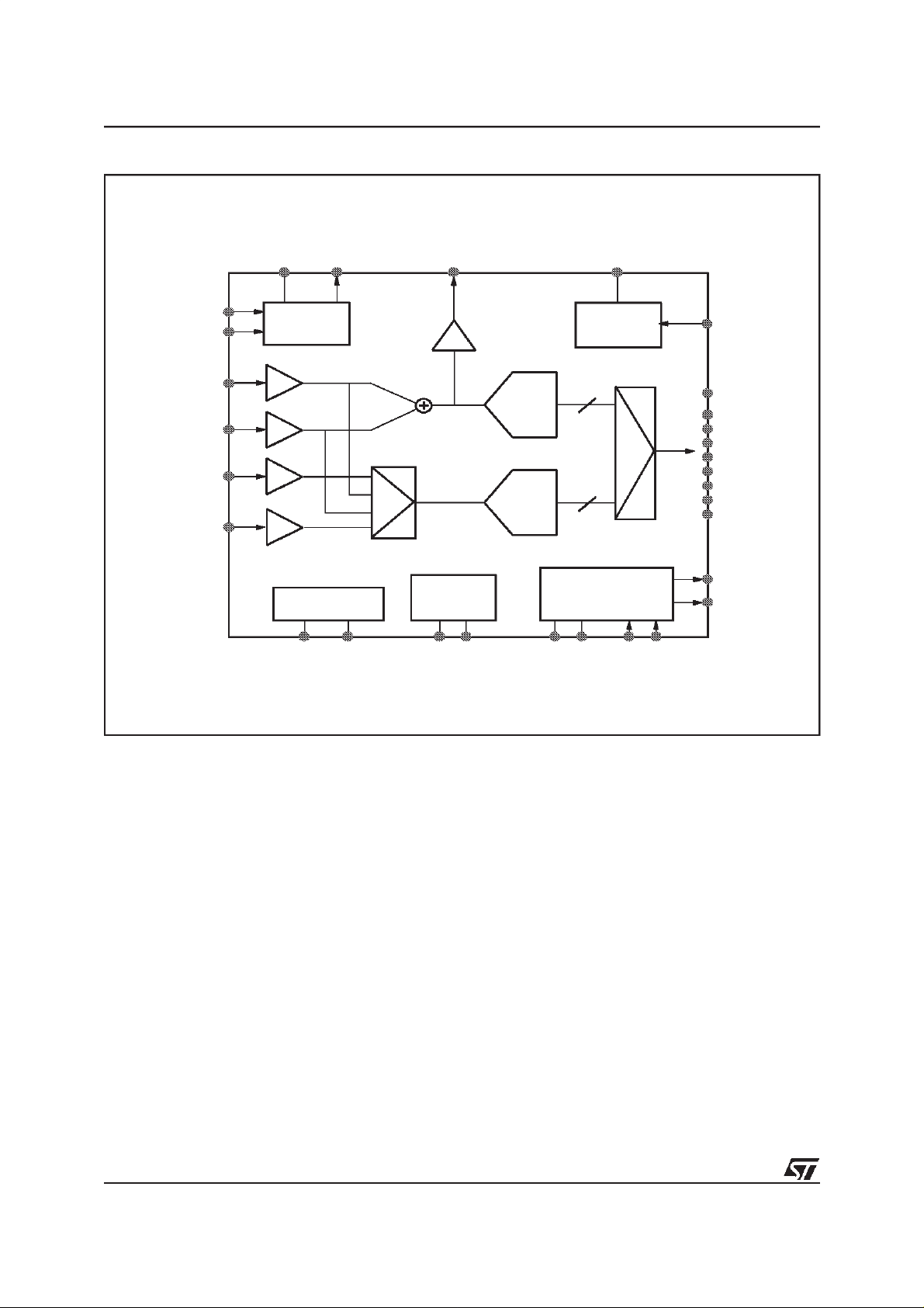
Figure 1. TDA7521 Block Diagram
REF IN
PON
AC
BD
E
F
REF
REF OUT
HF MON
CLOCK
REXT
Gen
I/V
I/V
I/V
RF
RF
ADC
ADC
Servo
I/V
Laser
ControlI/F
SDA SCL LD MD DL DR
Driver
ADC
Output MUX
Stereo
DAC
MUTEL MUTER
FILT
CKIN
Mgr
SYNC
d0
d1
d2
d3
d4
d5
d6/OF
d7/UF
OUTL
OUTR
1.0 HARDWARE DESCRIPTION
1.1 Clock source and generation
The master clock to operate the device is 768×Fs (High Frequency mode, HFM) or 384×Fs (Low Frequen-
cy mode, LFM). Fs=44.1KHz for CD applications. In either case, the clock is generated by TDA7522: an
internal low-jitter Charge-Pump PLL (CPPLL) and a Finite State Machine (FSM) synthesize all the needed
clocks for the internal blocks: a 512×Fs for the DAC and three 384×Fs (HFM) or 192×Fs (LFM), with dif-
ferent phases for ADCs and output digital multiplexer. The required loop filter network is made up of a
160pF capacitor from FILT to GND_pll in parallel with the series of a 10nF and a 4KΩ resistor. All clock-
related setups are communicated to TDA7521 via UART interface.
1.2 Voltage references
REFIN is an internal voltage reference generated by a resistor divider between VCC_dac and VSS_dac.
Nominal value (with VCC_dac=5V) is REFIN=2.5V. Careful filtering of this pin is essential; recommended
value of external capacitor is 47µF paralleled with 100nF ceramic. REFOUT is a 2.5V (nominal) buffered
output to bias the pickup. All the internal voltage references for ADCs and DACs are generated by bandgap-based circuits, thus allowing to reduce the noise induced by the power supply.
2/11

TDA7521
1.3 Laser driver section
The laser driver system is composed by the pick-up, the laser driver and the external PNP bipolar transistor. It controls the external pick-up current level (up to 100mA) through its base current in order to maintain
a certain amount of diode power emission, independently from temperature and aging effects. This is done
in a digital way by using a 6-bit DAC to set the monitor diode analog reference voltage at a constant level
(and so the current in the laser diode). Thus, 26-1 different bias currents (with relative monitor voltage between 100 and 300mV) can be selected via UART interface. A negative feedback loop sets both the monitor diode voltage and the laser diode bias current.
1.4 Preamplifier section
The goal of this section is to free the four voltage signals coming from either the CD pickup itself (voltage
inputs) or the internal current-to-voltage converters (current inputs) from their intrinsic DC component and
to amplify them to a level suitable for efficient A/D conversion. In case of current inputs, four transimpedance amplifiers convert the currents from AC (A+C), BD (B+D), E andF inputs intooutput voltages suitable
for the programmable preamplification chain; otherwise, this stage is by-passed and the voltageinputs are
directly connected to the preamplification stage. The two paths (for input current or input voltage) are digitally selected via UART interface. In the same way also the gain of the path and the offset cancellation for
the preamplification chain are controlled (the gain programmability range is spanning from 6 up to 29.5dB
in 48 discrete steps of 0.5dB each, while the offset nulling circuit allows a minimum correction step of about
22mV via a 6-bit DAC). Moreover the preamplification chain generates an HF signal, which carries the encoded audio data and is obtained by combining the photo-detector outputs as A+B+C+D. All these signals
(AC, BD, E, F and HF), which can be evaluated by means of the monitor output, are fed to the ADC section.
1.5 ADC section
The HF and servo (AC, BD, E and F) paths are digitized by means of two ADCs: the former (8-bit resolution, interleaved comparator two step architecture) samples theHF signal at a frequency of 384×Fs (HFM)
or 192×Fs (LFM), the latter (6-bit resolution, interleaved comparator two step architecture) allows to multiplex the data for the servo path (AC, BD, E and F) in an only analog signal AC/BD/E/F and samples this
signal at 384×Fs (HFM) or 192×Fs (LFM); that means each servo signal is sampled at 96×Fs or 48×Fs).
Then both the bitstreams (HF and AC/BD/E/F) are digitally multiplexed in a single bitstream (AC/HF/BD/
HF/E/HF/F/HF). A SYNC signal (high during the period of HF before AC output) is provided in order to
point out the start of a new frame. It is worth noting that output data change on the falling edge of the master clock.
The Table 1 shows the output data format for the ADC section: referring to AC/HF/BD/HF/E/ HF/F, the HF
signal have an
the servo path (AC, BD, E and F) have a different format:
from the preamplifiers plus underflow and overflow
8-bit format which represents the digitized value of the HF analog signal
6 bit for the digitized value of the analog output
(1)
.
, while the data for
Table 1. TDA7521 Output Format
LSB MSB
D0 D1 D2 D3 D4 D5 D6/UF D7/OF
Note: 1. Overflow and Underflow for the HF ADC are latched by a dedicated FSM and read via UART interface.
1.6 DAC section
In TDA7521 are present two 3rd order SC smoothing filters to be used in Digital-to-Analog conversion. Its
input signal is a bitstream created by a 2nd order digitalΣ∆modulator present in TDA7522. From there
3/11

TDA7521
the bitstream is passed to the analog chip and properly processed by the filter. The filter exhibits 96dB
SNR and more than -80dB THD for a full scale input signal.
4/11
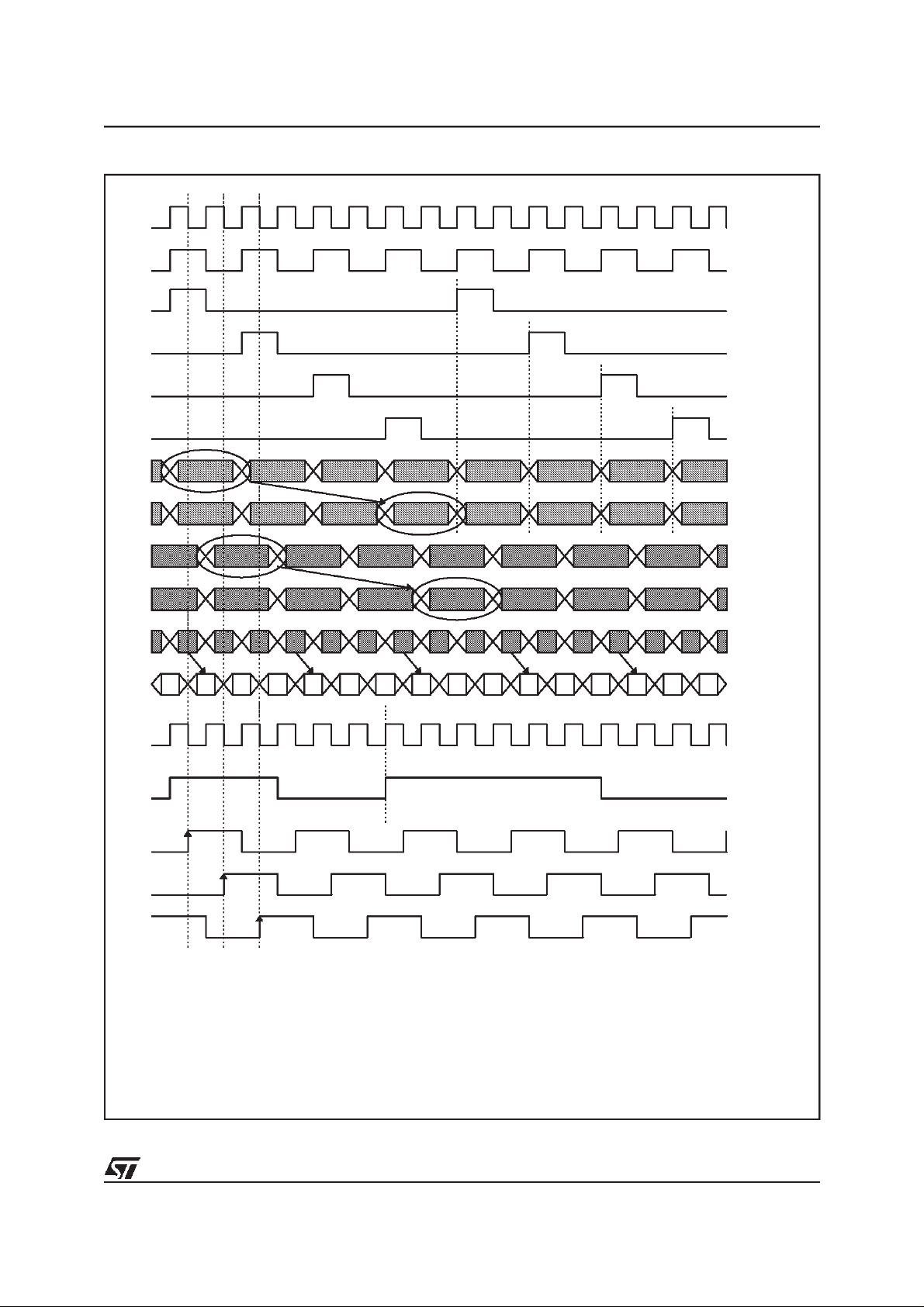
Figure 2. TDA7521 timings in 768×Fs mode
TDA7521
(1
(2
(3.A)
(3.B)
(3.C)
(3.D)
BDAC E F AC BD E F
BD E F AC BD E F
RF RF RF RF RF RF RF RF
RF RF RF RF RF RF RF RF
RBR ER FRARBR ER FR
ARBR ER FRARBR ER FR
(4
(5
(6
(7
(8
(9
(10)
(11)
(12.A)
(12.B)
Fig.3. A349 timing: (1) External clock (
rising edge, while RF data change on the falling edge); (3.A, 3.B, 3.C, 3.D) Internally generated
96×F
clocks for Servo ADC; (4) Servo data IN; (5) Servo data OUT; (6) RF data IN; (7) RF
S
data OUT; (8) AC/RF/BD/RF/E/RF/F/RF data stream before digital MUX; (9) Output
AC/RF/BD/RF/E/RF/F/RF; (10) Synthesized clock; (11) Generic Bitstream Input; (12.A, 12.B,
12.C) Possible synthesized
256× F
768× F
(depending on the initial conditions)
S
mode); (2) Servo clock (servo data change on its
S
(12.C)
5/11

TDA7521
2.0 FEATURE
The main performance of TDA7521 are reported below
Table 2. Main DC Characteristics (I)
Current input Condition Min Typ Max Unit
A+C diode input 1 16 µA
B+D diode input 1 16 µA
E diode input 1 16 µA
F diode input 1 16 µA
Table 3. Main DC Characteristics (II)
Voltage input Condition Min Typ Max Unit
A+C diode input 45 700 mVpp
B+D diode input 45 700 mVpp
E diode input 45 700 mVpp
F diode input 45 700 mVpp
The polarity of input signals can be defined by ST7 individually
Table 4. AC Main Performances
Contents Condition Min Typ Max Unit
DC offset range of each diode signals (*) Max input P-P 0 3/2 (*) mVpp
Frequency Range DC 4M MHz
Group delay Flatness 4 nsec
SNR 48 dB
Individual Gain Adjustment on AC, BD, E, F 0 23.5 dB
Gain Step range 0.5 dB
Individual OffsetAdjustment on AC, BD, E, F
MD (Monitor Diode) voltage range 100 300 mV
MD Adjustment Step 5 mV
6/11
TDA7521
Table 5. AC Main Performances
DAC Condition Min Typ Max Unit
Single end Output VCC/2 DC 1 Vrms
Frequency response 20 22K Hz
Dynamic Range 96 dB
THD@Full scale -80 dB
3.0 PIN FUNCTION
TDA7521 is housed in a 44 quad flat pack package; the related pin list is reported below.
Table 6. TDA7521 Pin List
Pin Number Name Pin Description
01 AC I A+C diode current input / voltage input DC coupled (1)
02 BD I B+D diode current input / voltage input DC coupled (1)
03 E I E diode current input / voltage input DC coupled (1)
04 F I F diode current input / voltage input DC coupled (1)
05 REXT I External Reference resistor (2)
06 REFOUT O Output Reference Voltage (5)
07 REFIN I VCC/2 Reference Voltage(4)
08 MUTER I Right Audio Channel Mute (6)
09 MUTEL I Left Audio Channel Mute (6)
10 PON I Power shutdown / Reset (7)
11 OUTR O Right Audio Channel Analog output (8)
12 VSS_DAC Gnd DAC Analog Ground
13 OUTL O Left Audio Channel Analog output (8)
14 VCC_DAC Vdd DAC Analog Supply (5V)
15 VDD_DAC Vdd DAC Digital Supply (5V)
16 GND_DAC Gnd DAC Digital Ground
17 Vss,DAC_Ref (3)
18 Vcc,DAC_Ref (3)
19 VDD_PLL Vdd PLL 5V Supply
20 FILT I/O PLL Loop Filter (9)
21 GND_PLL Gnd PLL Ground
22 CKIN I Master clock input
23 BSL I Digital Bit Stream input, Left Channel
7/11
TDA7521
Pin Number Name Pin Description
24 BSR I Digital Bit Stream input, Right Channel
25 SYNC O ADC Mux Sync output (10)
26 D7 O ADC output [MSB]
27 D6 O ADC output
28 D5 O ADC output
29 D4 O ADC output
30 D3 O ADC output
31 D2 O ADC output
32 D1/UF O (11)
33 D0/OF O (12)
34 GND_ADC Gnd ADC Ground
35 VDD_ADC Vdd ADC 5V Supply
36 GND_ADC Gnd ADC Ground
37 VCC_ADC Vdd ADC 5V Supply
38 SCK I ST7 Control I/F Clock input
39 SDA I/O ST7 Control I/F Data (14)
40 HFMON O HF output (13)
41 LD O Laser Control output (15)
42 MD I Monitor diode input
43 VSS_PRE Gnd Pre_AMP Ground
44 VCC_PRE Vdd Pre_AMP 5V Supply
Notes: 1. Current or Voltage input, DC coupled
2. Precision Resistor connected between Rext and ground
3. These pins are to be left unconnected
4. Internally generated, need external filtering cap
5. Buffered Vcc/2 Output
6. Driven by IC6D, active high
7. Dirven by IC6D, active low
8. 1 Vrms max., VCC/2 DC component
9. Needs RC-C externals network
10.High in correspondence of the HF sample preceding the AC one
11.LSB+1 of the HF ADC, Underflow bit of the servo one
12.LSB of the HF ADC, Overflow bit of the servo one
13.Can be selected among HF, AC, BD, E, F (via control interface)
14.Bidirectional, needs a pull-up resistor to 5 V line
15.Drives an external pnp.
8/11

TDA7521
4.0 TDA7521 REGISTERS ADDRESS MAP
Inside TDA7521 there are 16 registers that are to programmed by TDA7522; table nr.9 report the list. All
registers are 8 bit wide.
Table 7. TDA7521 registers Map
Address Register
0000 AC Gain reg
0001 BD Gain reg
0010 E Gain reg
0011 F Gain reg
0100 AC Offset Adjustment reg
0101 BD Offset Adjustment reg
0110 E Offset Adjustment reg
0111 F Offset Adjustment reg
1000 Monitor Output reg
1001 Laser Driver reg
1010 PLL reg
1011 Overflow reg (read only)
1100 Testmode register
1101 --unused-1110 Every Gain reg *
1111 Every Offset reg *
Note: 1. With these two configuration the data sent to the slave section is written inside every Gain/Offset register. This function can thus
.
be used to have a quick and global programming of the afore said register.
9/11
TDA7521
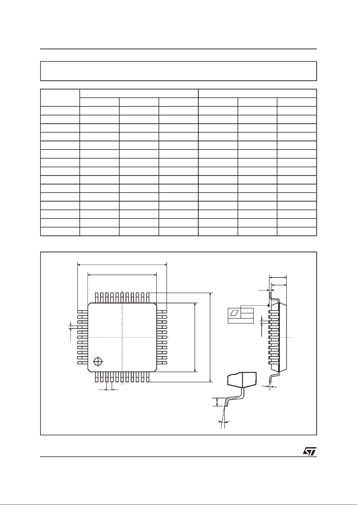
TQFP44 - 44 lead Quad Flat Package
Symb
Min Typ Max Min Typ Max
mm inch
A 1.60 0.063
A1 0.05 0.15 0.002 0.006
A2 1.35 1.40 1.45 0.053 0.055 0.057
B 0.30 0.37 0.45 0.012 0.014 0.018
C 0.09 0.20 0.004 0.008
D 12.00 0.472
D1 10.00 0.394
D3 8.00 0.315
e 0.80 0.031
E 12.00 0.472
E1 10.00 0.394
E3 8.00 0.315
L 0.45 0.60 0.75 0.018 0.024 0.030
L1 1.00 0.039
k0°3.5° 7° 0° 3.5° 7°
D
D1
A1
A
A2
34
B
44
Drawing is not to scale.
10/11
2333
22
E
E1
12
1
e
11
L
TQFP4410
0.10mm
.004
Seating Plane
B
C
K

TDA7521
.
Information furnished is believed to be accurate and reliable. However, STMicroelectronics assumes no responsibility for the consequences
of use of such information nor for any infringement of patentsor other rightsofthird parties which mayresult from its use. No license is granted
by implication or otherwise under any patent or patent rights of STMicroelectronics. Specifications mentioned in this publication are subject
to change without notice. This publication supersedes and replaces all information previously supplied. STMicroelectronics products are not
authorized for use as critical components in lifesupport devices or systems without express writtenapproval of STMicroelectronics.
The ST logo is a registered trademark of STMicroelectronics
1998 STMicroelectronics - All Rights Reserved
Australia - Brazil - Canada - China - France - Germany - Italy - Japan - Korea - Malaysia - Malta - Mexico - Morocco - The Netherlands -
Singapore - Spain - Sweden - Switzerland - Taiwan - Thailand - United Kingdom - U.S.A.
STMicroelectronics GROUP OF COMPANIES
11/11
 Loading...