

RF-FRONTEND FOR AM/FM-DSP- CARRADIOS
■
RF AGC generation by RF and IF detection
■
I/Q Mixer for FM IF 10.7MHz with image
rejection and programmable IF tank adjust for
FM and AM
■
Preamplifier and mixer for IF 10.7MHz AM
upconversion
■
VCO and programmable divider for “world
receiver”
■
Programmable controlled IF-gain stage
Additional features:
■
High performance fast PLL for RDS-system
■
Electronic alignment for the preselection stages
■
All functions bus-controlled
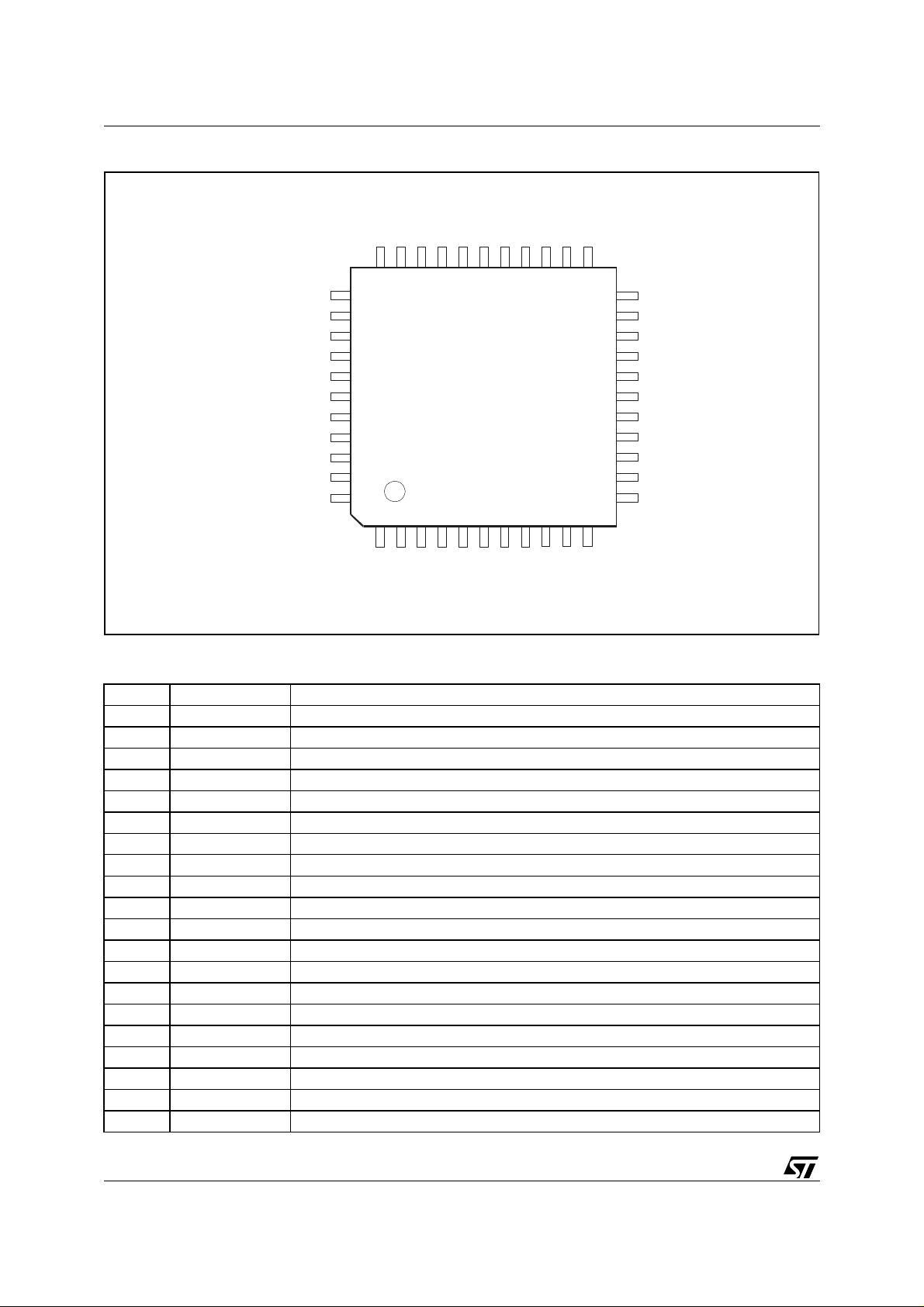
DESCRIPTION
The frontend is a high performance tuner circuit for
TDA7515
WITH IF SAMPLING
PRODUCT PREVIEW
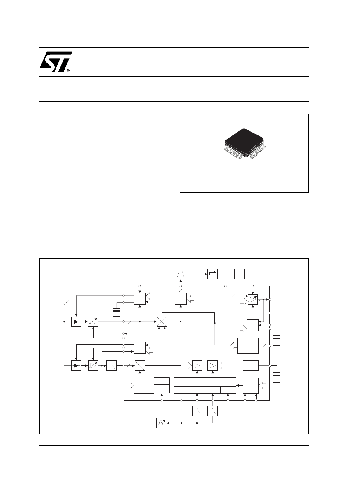
TQFP44
ORDERING NUMBER: TDA7515
AM/FM - DSP carradios with 10.7MHz - IF sampling.
It contains mixer and IF amplifiers for AM and FM,
VCO and PLL synthesizer on a single chip.
Use of BICMOS technology allows the implementa-
tion of several tuning function s and a minimum of external components.
1 BLOCK DIAGRAM
FM
PM
AM
PM
AGC ADJ
2
I
AGC
2
DIV
1/6
1/10
:1/:2/:3
VCO
1/4
1/8
2
Q
TV1 TV2
PLL
LPOUT LPAM LPFM LPHC
optional
2
Interface
AGC
Bus
Supply
REFDIV
Fref
18/100kHz
2
IF 10.7MHz
DAGC
2
00AT0037
July 2002
This is preliminary information on a new product now in development. Details are subject to change without notice.
1/5
TDA7515
2 PIN CONNECTION
IFAGCTC
VCCIF
IFOUT1
IFOUT2
IFGND
DAGC
Vref
Fref+
Fref-
IFAMAGCTC
SDA
00AT0036
33 32 31 30 29 28 27 26
VCC SCL
IFINAM
GND
IFIN1
IFIN2
MIXOUT1
MIXOUT2
AMAGCTC
FMIFAGCin
AMIN2
AMIN1
34
35
36
37
38
39
40
41
42
43
1 234567
FMPINDR
AMPINDR
AMRFAGCin
AMRFAGCout
FMIN1
RFGND
25 24 23
8910 11
TV1
FMIN2
FMAGCTC
22
21
20
19
18
17
16
15
14
13
1244
TV2
VCCVCO
3 PIN DESCRIPTION
Pin No. Pin Name Function
1 AMRFAGCin AM AGC Input for RF detection
2 AMRFAGCout AM AGC output for RF AGC
3 AMPINDR AM AGC PIN-diode driver
4 FMPINDR FM AGC Pindiode driver
5 FMIN1 FM Mixer Input 1
6 RFGND RF Ground
7 FMIN2 FM Mixer Input 2
8 FMAGCTC FM AGC time constant
9 TV1 Tuning voltage 1 output
10 TV2 Tuning voltage 2 output
11 VCCVCO Supply Voltage VCO
12 GNDVCO VCO Ground
13 VCOB Base VCO
14 VCOE Emitter VCO
15 VPLL PLL Supply Voltage
16 LPAM/SW OP AMP Input to PLL Loop Filter AM / switch output (optional)
17 LPOUT OPAMP output to PLL Loop Filter
18 LPREF Voltage Reference for PLL
19 LPFM OP AMP Input to PLL Loop Filter FM
20 LPHC High Current PLL Loop Filter
GNDPLL
LPHC
LPFM
LPREF
LPOUT
LPAM/SW
VPLL
VCOE
VCOB
GNDVCO
2/5
TDA7515
3 PIN DESCRIPTION
(continued)
Pin No. Pin Name Function
21 GNDPLL PLL Ground
22 SCL Bus connection (IIC clock)
23 SDA Bus connection (IIC data)
24 IFAMAGCTC Time constant for AM IF AGC
25 Fref- Reference frequency input
26 Fref+ Reference frequency input
27 Vref Reference voltage 5V
28 DAGC Digital keying AGC input
29 IFGND IF Ground
30 IFOUT2 IF amplifier output
31 IFOUT1 IF amplifier output
32 VCCIF Supply voltage for IF output
33 IFAGCTC IF AGC time constant
34 VCC Supply voltage
35 IFINAM IF input for narrowband AM
36 GND Ground
37 IFIN1 IF Input - signal
38 IFIN2 IF Input - blocked
39 MIXOUT1 Mixer Output
40 MIXOUT2 Mixer Output
41 AMAGCTC AM AGC time constant
42 FMIFAGCin IF input for FM AGC
43 AMIN2 AM RF Input
44 AMIN1 AM RF Input
4 THERMAL DATA
Symbol Parameter
R
T
th(j-a)
amb
T
stg
Thermal resistance 85 °C/W
Ambient temperature -40 85 °C
Storage temperature -55 150 °C
Min. Typ. Max.
Values
5 ABSOLUTE MAXIMUM RATINGS
Symbol Parameter Value Unit
V
CCIF
V
PLL
V
CCVCO
V
CC
V
MIXOUT1/2
Supply voltage for IF-interface 12 V
PLL supply voltage 12 V
VCO supply voltage 12 V
Supply voltage 12 V
Open collector voltage 12 V
Unit
3/5
TDA7515
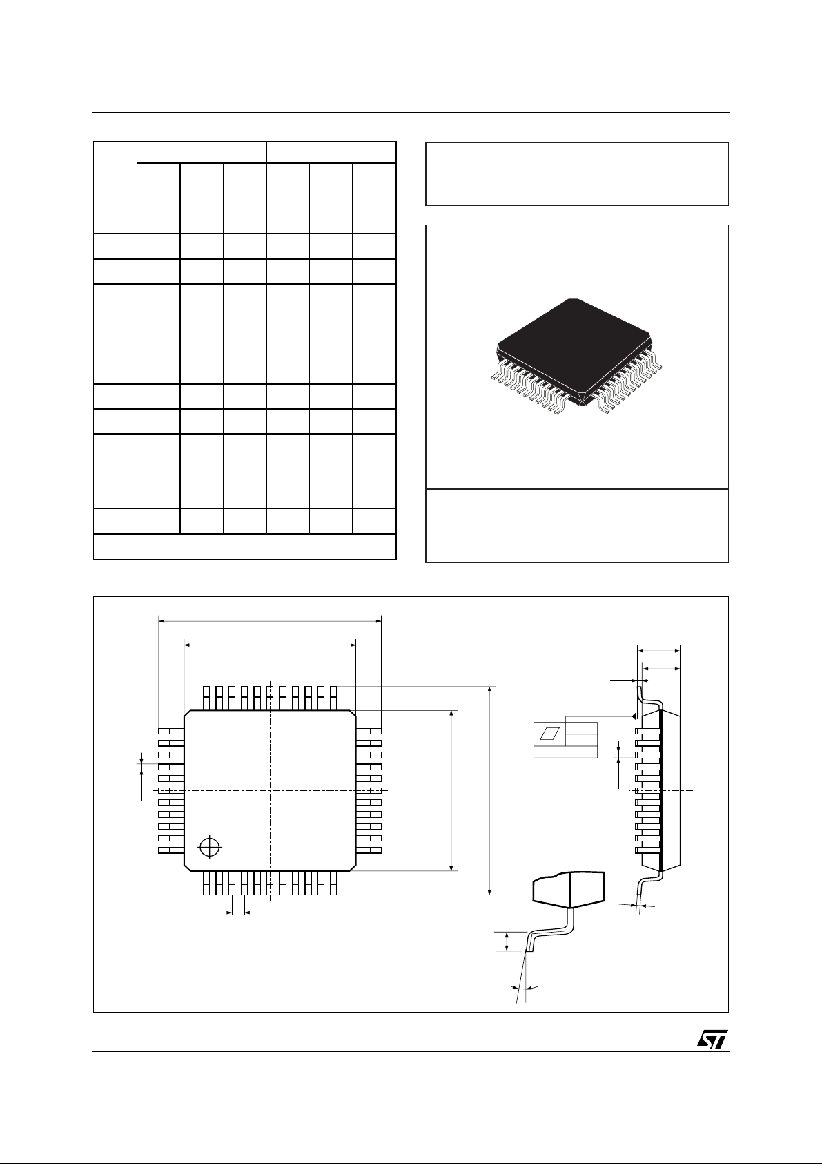
DIM.
mm inch
MIN. TYP. MAX. MIN. TYP. MAX.
A 1.60 0.063
A1 0.05 0.15 0.002 0.006
A2 1.35 1.40 1.45 0.053 0.055 0.057
B 0.30 0.37 0.45 0.012 0.014 0.018
C 0.09 0.20 0.004 0.008
D 12.00 0.472
D1 10.00 0.39 4
D3 8.00 0.315
e 0.80 0.031
E 12.00 0.472
E1 10.00 0.394
E3 8.00 0.315
L 0.45 0.60 0.75 0.018 0.024 0.030
L1 1.00 0.039
K 0°(min.), 3.5˚(typ.), 7°(max.)
OUTLINE AND
MECHANICAL DATA
TQFP44 (10 x 10)
D
D1
A1
2333
34
B
44
1
e
22
E
E1
12
11
0.10mm
.004
Seating Plane
B
A
A2
C
L
K
TQFP4410
4/5

TDA7515
Information furnished is believed to be accurate and reliable. However, STMicroelectronics assumes no responsibility for the consequences
of use of such information nor for any infringement of patents or other rights of third parties which may result from its use. No license is granted
by implic ation or o th erwise un der any patent or patent ri ghts of STM i croelectronics. Specifications mentioned in this p ublication are subject
to change without notice. This publication supersedes and replaces all information previously supplied. STMicroelectronics products are not
authorized for use as c ri t i cal components in life support dev i ces or systems without express wri t ten approval of STMic roelectronics.
The ST logo is a registered trademark of STMicroelectronics
© 2002 STMic roelectroni cs - All Rights Reserved
Australia - Brazi l - Canada - Ch i na - F i nl and - Franc e - Germany - Hong Kong - India - Isr ael - Italy - Japan -Malay si a - Malta - Morocco -
Singap ore - Spain - Sweden - Swit zerland - U ni ted Kingdom - United S tates.
STMicroelectronics GROUP OF COMPANIES
http://www.s t. com
5/5
 Loading...