


AM/FM CAR RADIO TUNER IC WITH INTELLIGENT
FM-PART
■ RF AGC GENERATION BY RF AND IF
DETECTION
■ I/Q MIXER FOR 1S T FM IF 10.7MHz WIT H
IMAGE REJECTION
■ 2 PROGRAMMABLE IF-GAIN STAGES
■ MIXER FOR 2
■ INTERNAL 450KHz BANDPASS FILTER WITH
THREE BANDWIDTHS CONTROLLED BY ISS
■ FULLY INTEGR ATED FM-DEMODULATOR
WITH NOISE CANCELLATION
AM-PART
■ WIDE AND NARROW AGC GENERATION
■ PREAMPLIFIER AND MIXER FOR 1ST IF
10.7MHz, AM UPCONVERSION
■ MIXER FOR 2
■ INTEGRATED AM-DEMODULATOR
■ OUTPUT FOR AM-STEREO-DECODER
ADDITIONAL FEATURES
■ VCO FOR WORLD TUNING RANGE
■ HIGH PERFORMANCE FAST PLL FOR RDS-
SYSTEM
■ IF COUNTER FOR FM AND AM WITH
SEARCH STOP SIGNAL
■ QUALITY DETECTOR FOR LEVEL,
DEVIATION, ADJACENT CHANNEL AND
MULTIPATH
■ QUALITY DETECTION INFORMATIONS AS
ANALOG SIGNALS EXT ERN AL AVAIL ABLE
nd
IF 450KHz
nd
IF 450KHz
TDA7512
SELECTIVITY SYSTEM (ISS)
PRELIMINARY DATA
TQFP64
ORDERING NUMBER: TDA7512
■
ISS (INTELLIG ENT SELECTIVITY SYSTEM)
FOR CANCELLATION OF ADJACENT
CHANNEL AND NOISE INFLUENCES
■ ADJACENT CHANNEL MUTE
■ FULLY ELECTR ONIC ALIGNMENT
■ ALL FUNCTIONS I
■ ISS FILTE R STATUS I NFORMATION I
READABLE
DESCRIPTION
The TDA7512 is a high performance tuner circuit for
AM/FM car radio. It contains mixer, IF amplifier, demodulator for AM and FM, q uality detection, ISS filter
and PLL synthesizer with IF count er on a single c hip.
Use of BICMOS technology allows the implementation of several tuning function s and a mini mum of external components.
2
C-BUS CONTROLLED
2
C-BUS
September 2003
This is preliminary information on a new product now in development or undergoing evaluation. Details are subject to change without notice.
1/42
TDA7512
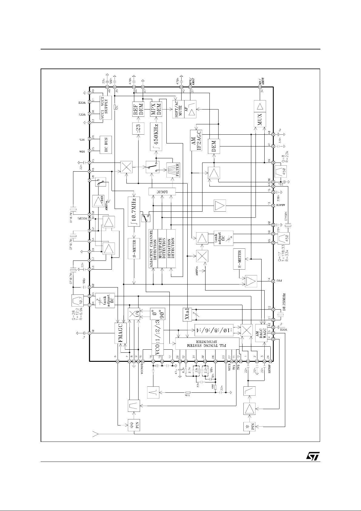
BLOCK DIAGRAM
2/42
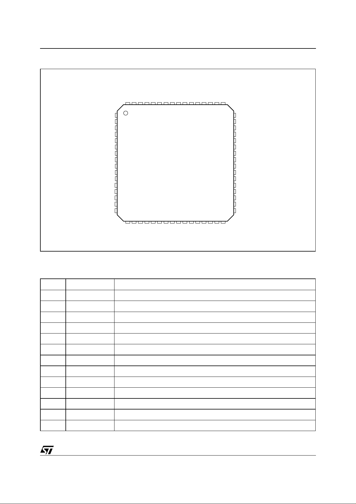
PIN CONNECTION (Top view )
AMMIX1IN2
AMMIX1IN1
AMRFAGCIN
AMRFAGCOUT
AMPINDR
FMPINDR
FMMIX1IN1
GNDRF
FMMIX1IN2
FMAGCTC
TV1
TV2
ADJCH
FSU
ISSTC
VCCVCO
MIX1OUT2
MIX1OUT1
63
64
1
2
3
4
5
6
7
8
9
10
12
13
14
15
16
17 18 19 20 21
VCCIF1
AMRFAGCTC
60
61
62
GNDIF1
AMIF1IN/ISS
FMAMP1IN
AMMIX2OUT1
FMAMP1OUT
AMMIX2OUT2
FMIF1REF
FMAMP2IN
FMIF1AGCIN
59 58 57 56 5455 53 52 51 50 49
22 23 24 25 26
271128 29 30 31 32
VCC2
FMAMP2OUT
GNDVCC2
48
47
46
45
44
43
42
41
40
39
38
37
36
35
34
33
TDA7512
VREF1
GNDDEM
FMMIX2IN1
FMMIX2IN2
REFDEMC FM/AM
AMIF2IN
MUTETC
AMDETC
AMAGC2TC
AMIFBPF
AMIFREF
MPX/AFAM
VCC1
FSW
AMST/MP
GNDVCC1
SCL
SDA
VCOB
GNDVCO
VCOE
XTALG
DEVTC
XTALD
GNDVCC3
SSTOP
VCC3
LPOUT
PIN DESCRIPTI ON
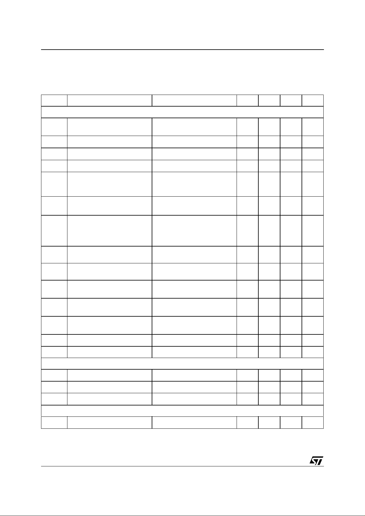
N° Pin Name Function
1 AMMIX1IN2 AM Input2 Mixer 1
2 AMMIX1IN1 AM Input1 Mixer 1
3 AMRF AGCIN Input AM RF AGC
4 AMRFAGCOUT Output AM RF AGC
5 AMPINDR AM PIN Diode Driver Output
6 FMPINDR FM PIN Diode Driver Output
7 FMMIX1IN1 FM Input1 Mixer1
8 GNDRF RF Ground
9 FMMIX1IN2 FM Input2 Mixer1
10 FMAGCTC FM AGC Time Constant
11 TV1 Tuning Voltage Preselection1
LPAM
VREF2
LPFM
LPHC
TQFP64
12 TV2 Tuning Voltage Preselection2
13 ADJCH Ident. Adjacent Channel Output
3/42

TDA7512
PIN DESCRIPTI ON (continued)
N° Pin Name Function
14 FSU Unweighted Fieldstrength Output
15 ISSTC Time Constant for ISS Filter Switch
16 VCCVCO VCO Supply
17 GNDVCO VCO Ground
18 VCOB VCO Input Base
19 VCOE VCO Output Emitter
20 DEVTC Deviation Detector Time Constant
21 XTALG Xtal Oscillator to MOS Gate
22 XTALD Xtal Oscillator to MOS Drain
23 GNDVCC3 VCC3 Ground
24 SSTOP Search Stop Output
25 SDA
26 SCL
27 VCC3 Supply Tuning Voltage
28 LPOUT O p Amp O u tput to PLL Loop Filters
29 VREF2 Voltage Reference for PLL Op Amp
30 LPAM Op Amp Input to PLL Loop Filters AM
31 LPFM Op Amp Input to PLL Loop Filters FM
32 LPHC High Current PLL Loop Filter Input
33 GNDVCC1 Digital Ground
34 AMST/MP AM Stereo Out / Ident. Multipath Output
35 FSW Weighted Fi eldstrength Output
36 VCC1 Digital Supply
37 MPX/AFAM MPX Output / AM AF Out put
38 AMI FREF Reference Voltage AM IF Amp
39 AMIFBPF AM IF Filter
40 AMAGC2TC AM AGC2 Time Constant
2
C-Bus Da ta
I
2
C-Bus Clock
I
41 AMDETC AM Detector Capacitor
42 MUTETC Softmute Time Constant
43 AMIF2IN Input AM IF2
44 REFDEMC FM/AM Demodulator Reference FM/AM
45 FMMIX2IN2 FM IF1 MIX2 Input1
4/42
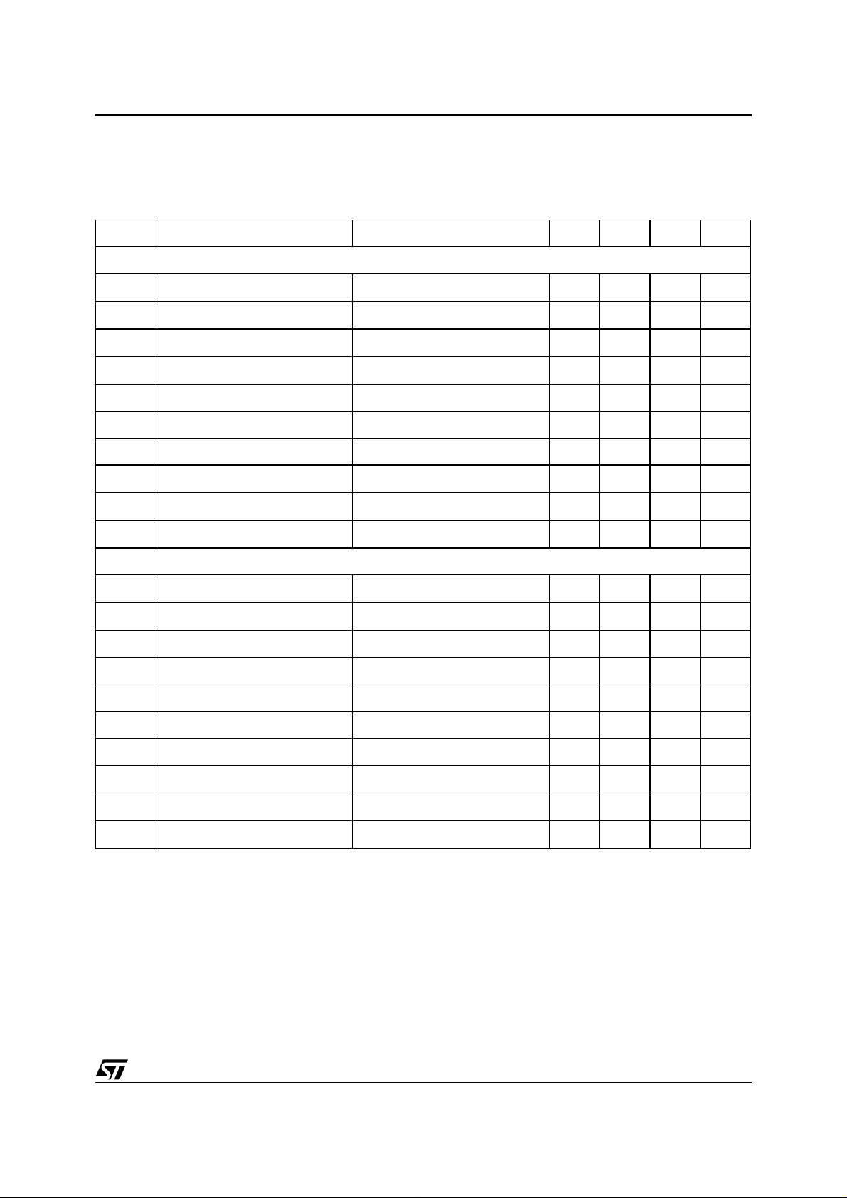
PIN DESCRIPTI ON (continued)
N° Pin Name Function
46 FMMIX2IN1 FM IF1 MIX2 Input2
47 GNDDEM Ground FM Demodul ator
48 VREF1 Reference 5V
49 GNDVCC2 Analog Ground
50 FMAMP2OUT FM IF1 Amplifier2 Output
51 VCC2 Analog Supply
52 FMAMP2IN FM IF1 Amplifier2 Input
53 FMIF1REF FM IF1 Amplifier Reference
54 FMAMP1OUT FM IF1 Amplifier1 Output
55 AMMIX2OUT2 AM Tank 450kHz
56 AMMIX2OUT1 AM Tank 450kHz
57 FMAMP1IN FM IF1 Amplifier1 Input
58 AMIF1IN/ISS AM IF1 Input/ISS filter status
TDA7512
59 GNDIF1 FM IF1 Ground
60 FMIF1AGCIN FM IF1 AG C Input
61 VCCIF1 IF1 Supply
62 AMRFAGCTC AM RF AGC Time Constant
63 MIX1OUT2 MIX Tank 10.7MHz
64 MIX1OUT1 MIX Tank 10.7MHz
THERMA L D ATA
Table 1.
Symbol Parameter Value Unit
R
th(j-a)
Thermal resistance junction to ambient 68 max. °C/W
ABSOLUTE MAXIMUM RATINGS
Table 2.
Symbol Parameter Value Unit
V
T
amb
T
stg
Supply Voltage 10.5 V
S
Ambient Temperature -40 to 85 °C
Storage Temperature -55 to +150 °C
5/42
TDA7512
Table 3. ELECTRICAL CHARACTERISTICS
T
= +25°C, V
amb
f
=1kHz, f
MOD
specified.
Symbol Parameter Test Condition Min. Typ. Max. Unit
Supply
= V
CC1
IF1
CC2
=10.7MHz, f
= V
= V
CC3
=450KHz, f
IF2
CCVCO
= V
= V
CCMIX1
= 10.25MHz, in application circuit, unless otherwise
Xtal
=8.5V, fRF= 98MHz, dev. = 40kHz,
CCIF1
V
CC1
V
CC2
V
CC3
V
CCVCO
V
CCMIX1
V
CCMIX2
V
CCIF1
I
CC1
I
CC1
I
CC2
I
CC2
I
CC3
I
CCVCO
I
CCMIX1
I
CCMIX1
Digital supply voltage 7.5 8.5 10 V
Analog supply voltage 7.5 8.5 10 V
Analog tuning voltage 7.5 8.5 10 V
VCO supply voltage 7.5 8.5 10 V
MIX1 supply voltage 7.5 8.5 10 V
MIX2 supply voltage 7.5 8.5 10 V
IF1 supply voltage 7.5 8.5 10 V
Supply current FM ON 7.5 mA
Supply current AM ON 10 mA
Supply current FM ON / VCO:3 70 mA
Supply current AM ON 70 mA
Supply current 2 mA
Supply current 9 mA
Supply current FM ON 8 mA
Supply current AM ON 7 mA
I
CCMIX2
I
CCIF1
Supply current AM ON 7 mA
Supply current 6 mA
Reference Voltages
V
V
REF1
REF2
Internal reference voltage I
Internal reference voltage I
Wide Band RF AGC
V
V
Lower threshold start V10 = 2.5V 85
7-9
Upper threshold start V10 = 2.5V 96
7-9
Narrow Band IF & Keying AGC
V
V
Lower threshold start KAGC = off, V
60
Upper threshold start KAGC = off, V
60
6/42
= 0mA 5 V
REF1
= 0mA 2.5 V
REF2
7-9
7-9
= 0mV
= 0mV
RMS
RMS
86
98
dB
dB
dB
dB
µV
µV
µV
µV
TDA7512
Table 3. ELECTRICAL CHARACTERISTICS (continued)
T
= +25°C, V
amb
f
=1kHz, f
MOD
specified.
Symbol Parameter Test Condition Min. Typ. Max. Unit
= V
CC1
IF1
CC2
=10.7MHz, f
= V
= V
CC3
=450KHz, f
IF2
CCVCO
= V
= V
CCMIX1
= 10.25MHz, in application circuit, unless otherwise
Xtal
=8.5V, fRF= 98MHz, dev. = 40kHz,
CCIF1
V
V
R
C
Lower threshold start with KAGC KAGC = max, V
60
Startpoint KAGC KAGC = max, V
35
Control range KAGC
∆
Input resistance 10
IN
Input capacitanc e 2.5 pF
IN
AGC Time Constant Output
V
V
Max. AGC output voltage V
10
Min. AGC output voltage V
10
I
Min. AGC charge current V
10
I
Max. AGC discharge current V
10
AGC PIN Diode Driver Output
AGC OUT, current min. V
I
6
I
AGC OUT, current max. V
6
= 0mV
∆f
=300KHz
IF
∆f
=300KHz
IF
f
generate FSW level at V
IF1
∆V
= +0.4V
35
= 0mV
7-9
= 50mV
7-9
= 0mV
7-9
= 50mV
7-9
= 0mV
7-9
= 50 mV
7-9
7-9
= 0mV
7-9
RMS
RMS
RMS,V10
RMS
= 2.5V -12.5
RMS,V10
, V6 = 2.5V 50
, V6 = 2.5V -20 mA
RMS
RMS,
RMS,
35
98
3.6 V
dB
16 dB
Ω
k
V
+V
REF1
BE
V
0.5 V
µA
= 2.5V 1.25 mA
µA
µV
I/Q Mixer1 (10.7MHz)
R
C
R
V
g
CP
Input resistance differential 10
IN
Input capacitanc e differential 4 pF
IN
Output resistance differential 100
OUT
Input dc bias 3.2 V
7,9
Conversion transconductance 17 mS
m
F Noise figure
1dB compression point referred to diff. mixer input 100
1dB
Ω generator resistance
400
3dB
IIP3 3rd order intermodulation 122
IQG I/Q gain adjust G -1 +1 %
IQP I/Q phase adjust PH -7 +8 DEG
IRR Image rejection ratio ratio wanted/image 30 40 dB
IRR Image rejection ratio with gain and phase adjust 40 46 dB
dB
dB
k
k
Ω
Ω
µV
µV
7/42
TDA7512
Table 3. ELECTRICAL CHARACTERISTICS (continued)
T
= +25°C, V
amb
f
=1kHz, f
MOD
specified.
Symbol Parameter Test Condition Min. Typ. Max. Unit
IF1 Amplifier1 +2 (10.7MHz)
= V
CC1
IF1
CC2
=10.7MHz, f
= V
= V
CC3
=450KHz, f
IF2
CCVCO
= V
= V
CCMIX1
= 10.25MHz, in application circuit, unless otherwise
Xtal
=8.5V, fRF= 98MHz, dev. = 40kHz,
CCIF1
G
G
R
R
CP
IIP3 3rd order Intermodulation
Min. gain IFG 18 dB
min
Max. gain IFG
max
Input resistance 330
IN
Output resistance 330
OUT
1dB compression point
1dB
referred to 330
referred to 330
Ω input
Ω input
26
105
126
Mixer2 (450kHz)
R
V
V
Input impedance 330
IN
Max. input voltage 900 mV
46
Limiting sensitivity S/N = 20dB 25
48
G Mixer gain 18 dB
Limiter 1 (450kHz)
G
Limiter
Gain 80 dB
Demodulator, Audio Output
THD Dev.= 75kHz, V
= 10mV
46
RMS
0.1 %
dB
Ω
Ω
dBµV
dBµV
Ω
RM
S
µV
V
R
|∆V|
∆V|
|
MPX output signal Dev.= 75kHz 500 mV
MPX
Output resistance 50
OUT
DC offset fine adjust DEM, MENA=1 8.5 mV
min
DC offset fine adjust DEM, MENA=1 264 mV
max
S/N Dev.= 40kHz,V
Quality Detection
S-meter, Unweighted Fieldstrength
V
V
V
∆V
∆V
Min. input voltage MIX2 10
46
Fieldstrength output V46 = 0V
14
Fieldstrength output V46 = 1V
14
voltage per decade SMSL = 0 1 V
14
voltage per decade SMSL = 1 1.5 V
14
8/42
RMS
RMS
= 10mV
46
RMS
RM
S
Ω
76 dB
µV
0.1 V
4.9 V
TDA7512
Table 3. ELECTRICAL CHARACTERISTICS (continued)
T
= +25°C, V
amb
f
=1kHz, f
MOD
specified.
Symbol Parameter Test Condition Min. Typ. Max. Unit
= V
CC1
IF1
CC2
=10.7MHz, f
= V
= V
CC3
=450KHz, f
IF2
CCVCO
= V
= V
CCMIX1
= 10.25MHz, in application circuit, unless otherwise
Xtal
=8.5V, fRF= 98MHz, dev. = 40kHz,
CCIF1
∆V
R
S-meter offset SL, SMSL=1 -15 15 dB
14
Output resistance 200
OUT
TK Temp coeff. 0 ppm/K
S-meter, Weighted Fieldstrength
R
V
V
OUT
Fieldstrength output V46 = 0V
35
Fieldstrength output V46 = 1V
35
RMS
RMS
Output resistance 12
2.5 V
4.9 V
Adjacent Channel Gain
G
G
Gain minimum ACG=0 32 dB
min
Gain maximum ACG=1 38 dB
max
Adjacent Channel Filter
f
f
f
-20dB
-3dB frequency highpass ACF=0 100 kHz
HP
Centre frequency ACF=1 100 kHz
BP
Attenuation 20dB 70 kHz
Adjacent Channel Output
V
Output voltage low 0.1 V
13
Ω
Ω
k
V
R
Output voltage high 4.9 V
13
Output resistance 4
OUT
Multipath Channel Gain
G
G
Gain minimum MPG=0 12 dB
min
Gain maximum MPG=1 23 dB
max
Multipath Bandpass Filter
f
Lower
f
Upper
Centre frequency low MPF=0 19 kHz
Centre frequency up MPF=1 31 kHz
Q Quality factor 5 10
Multipath Output
V
V
R
Output voltage low 0.1 V
34
Output voltage high 4.9 V
34
Output resistance 2.5
OUT
k
k
Ω
Ω
9/42

TDA7512
Table 3. ELECTRICAL CHARACTERISTICS (continued)
T
= +25°C, V
amb
f
=1kHz, f
MOD
specified.
Symbol Parameter Test Condition Min. Typ. Max. Unit
ISS (intelligent Selectivity System)
Filter 450kHz
= V
CC1
IF1
CC2
=10.7MHz, f
= V
= V
CC3
=450KHz, f
IF2
CCVCO
= V
= V
CCMIX1
= 10.25MHz, in application circuit, unless otherwise
Xtal
=8.5V, fRF= 98MHz, dev. = 40kHz,
CCIF1
f
centre
Centre frequency f
REF_intern
= 450kHz 450 kHz
BW 3dB Bandwidth, -3dB ISS80 = 1 80 kHz
BW
Bandwidth, -20dB ISS80 = 1 150 kHz
20dB
BW 3dB Bandwidth, -3dB ISS80 = 0 120 kHz
BW
Bandwidth, -20dB ISS80 = 0 250 kHz
20dB
BW 3dB Bandwidth weather band ISS30 = 1 30 kHz
BW
-20dB weather band ISS30 = 1 80 kHz
20dB
Adjacent Channel ISS Filter Threshold
V
V
V
V
Internal low threshold ACNTH 0 V
NTH
Internal high threshold ACNTH 0.3 V
NTH
Internal low threshold ACWTH 0.25 V
WTH
Internal high threshold ACWTH
WTH
0.95
Multipath Threshold
V
THMP
Internal low threshold MPTH 0.50 V
V
V
THMP
Internal high threshold MPTH 1.25 V
ISS Filter Time Constant
Charge current low mid TISS, ISSCTL = 1 -74
I
15
I
Charge current high mid TISS, ISSCTL = 1 -60
15
I
Charge current low narrow TISS, ISSCTL = 1 -124
15
I
Charge current high narrow TISS, ISSCTL = 1 -110
15
I
Discharge current low TISS, ISSCTL = 0
15
I
Discharge current high TISS, ISSCTL = 0 15
15
V
Low voltage ISSCTL = 0 0.1 V
15
10/42
µA
µA
µA
µA
1
µA
µA
TDA7512
Table 3. ELECTRICAL CHARACTERISTICS (continued)
T
= +25°C, V
amb
f
=1kHz, f
MOD
specified.
Symbol Parameter Test Condition Min. Typ. Max. Unit
= V
CC1
IF1
CC2
=10.7MHz, f
= V
= V
CC3
=450KHz, f
IF2
CCVCO
= V
= V
CCMIX1
= 10.25MHz, in application circuit, unless otherwise
Xtal
=8.5V, fRF= 98MHz, dev. = 40kHz,
CCIF1
V
High voltage ISSCTL = 1 4.9 V
15
ISS Filter Switch Threshold
V
15
V
15
V
15
V
15
I
20
I
20
I
20
I
20
DEV
DEV
RATIO
n
RATIO
Threshold ISS on ISSCTL = 0 3 V
Threshold ISS off ISSCTL = 0 1 V
Threshold ISS narrow on ISSCTL = 0 4 V
Threshold ISS narrow off ISSCTL = 0 2 V
Charge current low TDEV -20
Charge current high TDEV -34
Discharge current low TDEV 6
Discharge current high TDEV 20
Internal low threshold DWTH 30 kHz
WTH
Internal high threshold DWTH 75 kHz
WTH
Referred to threshold DTH 1
mi
Referred to threshold DTH 1.5
m
ax
Softmute
µA
µA
µA
µA
V
ANT
V
ANT
a
SMmin
a
SMmax
a
SMTHIS
S
V
ACTH
a
SMAC
I
42
I
42
S/N Over All
S/N
Upper startpoint SMTH, SMD, SLOPE = 0 10
lower startpoint SMTH, SMD, SLOPE = 0 3
Min. softmute depth SMD, SLOPE = 0, SMTH
Max. softmute depth SMD, SLOPE = 0, SMTH
Upper
Upper
18 dB
36 dB
dB
dB
Mute depth threshold for ISS filter onSMCTH 0.2 2 dB
Internal AC mute threshold ACM 60 340 mV
AC mute depth ACMD 4 10 dB
Charge current -47.5
Discharge current 2.5
V
ANT_min
= 60dBµV,
66 dB
µA
µA
dev.= 40kHz,LP=15KHz
deemphasis t = 50
µs
11/42
µV
µV
TDA7512
Table 4. ELECTRICAL CHARACTERISTICS
T
= +25°C, V
amb
30% AMf
V
antenna input).
INRF
= 10.7MHz, f
IF1
Symbol Parameter Test Condition Min. Typ. Max. Unit
Global
CC1
= V
= V
CC2
=450kHz, f
IF2
CC3
= V
= V
CCVCO
= 10.25MHz, in application circuit, (unless ot herwise noted,
xtal
CCMIX1
= V
=8.5V, fRF=1MHz, f
CCMIX2
MOD
= 400Hz at
ANT
Max. sensitivity
Ref.: V
= 60dBµV,
INRF
V
min
us Usable sensitivity (S+N)/N = 20 dB 30 26
V
ANT
∆V
(S+N)/N Signal to Noise Ratio
a
IF2 AGC Range
ANT
IF rejection
IF
Ref.: V
Ref.: V
Ref: V
= 60dBµV,
INRF
= 60ddBµV
INRF
= 60dBµV,
INRF
IF1 = 10.7MHz
IF2 = 450kHz
f
THD Total Harmonic Distortion
Frequency response
AF
Ref.: V
∆V
AF
V
INRF
= 60dBµV,
INRF
= -3 dB
= 60dBµV, m = 0.8
m = 0.3
V
= 120 dbµV, m = 0.8
INRF
m = 0.3
V
V
Output level
37
Output level
34
V
Min. RF AGC threshold
3
= 60dBµV
V
INRF
= 60dBµ, m=off
V
INRF
WAGC 90
Max. RF AGC threshold
19
dBµV
dB
56 dB
50 60 dB
100
100
3.6 kHz
0.5
0.3
1.0
0.3
220 mV
190 mV
dB
109
dB
µV
dB
dB
%
RM
S
RM
S
µV
µV
V
Min. IF AGC threshold
58
WAGC 90
Max. IF AGC threshold
V
Min. DAGC threshold
58
DAGC 74
Max. DAGC threshold
|I
| AGC2 charge current se ek 160
40max
CCR Charge current ratio seek/seek off 30
AGC Voltage Driver Output
Max. AGC output voltage 3.5 V
V
4
V
Min. AGC output voltage
4
| AGC current 100
| I
4
AGC PIN Diode Driver Output
AGC driver current -2 mA
I
5
12/42
109
96
0.5
dB
dB
dB
dB
µV
µV
µV
µV
µA
V
µA
TDA7512
Table 4. ELECTRICAL CHARACTERISTICS (continued)
T
= +25°C, V
amb
30% AMf
V
antenna input).
INRF
= 10.7MHz, f
IF1
Symbol Parameter Test Condition Min. Typ. Max. Unit
AM Mixer1 (10.7MHz)
CC1
= V
= V
CC2
=450kHz, f
IF2
CC3
= V
= V
CCVCO
= 10.25MHz, in application circuit, (unless ot herwise noted,
xtal
CCMIX1
= V
=8.5V, fRF=1MHz, f
CCMIX2
MOD
= 400Hz at
R
C
R
CP
IIP3 3rd order intermodulation 132
Input resistance differential 1.2
IN
Input capacitanc e differential 4 pF
IN
Output impedance differential 100
OUT
1dB compression point referred to diff. mixer input 115
1dB
Ω
k
Ω
k
µV
dB
dBµV
F Noise figure 8dB
A Gain 26 dB
Min. capacitance step IF1T 0.55 pF
min
Max. capacitance IF1T 8.25 pF
max
IF1T 2 pF
C
C
C
31-64
AM Mixer2 (450kHz)
R
C
CP
IIP3 3rd order intermodulation 132
Input resistance 10
58
Input capacitanc e 2.5 pF
58
1dB compression point referred to diff. mixer input 120
1dB
dB
dB
Ω
k
µV
µV
F Noise figure 12 dB
A Max. gain Mixer2 tank output 34 dB
Gain control range 20 dB
Min. cap step IF2T 1.6 pF
min
Max. cap IF2T 24 pF
max
IF2T 2 pF
C
C
∆A
C
55-56
13/42

TDA7512
Table 5. ADDITIONAL PARAMETERS
Symbol Parameter Test Condition Min. Typ. Max. Unit
Output of Tuning Voltages (TV1,TV2)
V
R
Output voltage TVO 0.5 V
OUT
Output impedance 20
OUT
Xtal Reference Oscillator
f
C
C
∆f/f
∆f/f
2
I
C-Bus interface
f
SCL
V
V
V
Reference frequency C
LO
Min. cap step XTAL 0.75 pF
Step
Max. cap XTAL 23.25 pF
max
Deviation versus VCC2
Deviation versus temp -40°C < T < +85°C 0.2 ppm/K
Clock frequency 400 kHz
Input low voltage 1V
IL
Input high voltage 3 V
IH
Input current -5 5
I
IN
Output acknowledge voltage IO = 1.6mA 0.4 V
O
Loop Filter Input/Output
-I
V
V
I
OUT
I
OUT
Input leakage current VIN = GND, PD
IN
I
Input leakage current VIN = VREF1
IN
Output voltage Low I
OL
Output voltage High I
OH
Output current, sink V
Output current, source V
Voltage Controlled Oscillator (VCO)
f
VCOmin
f
VCOmax
Minimum VCO frequency
Maximum VCO frequency 260 MHz
C/N Carrier to Noise
SSTOP Output (Open Collector)
V
V
-I
Output voltage low
24
Output voltage high 5V
24
Output leakage current V24 = 5V -0.1 0.1
24
I
Output current, sink V24 = 0.5V-5V 1 mA
24
= 15pF 10.25 MHz
Load
∆V
CC2
= 1V
= Tristate -0.1 0.1
OUT
1.5 ppm/V
-0.1 0.1
PD
= Tristate
OUT
= -0.2mA 0.05 0.5 V
OUT
= 0.2mA V
OUT
= 1V to V
OUT
= 1V to V
OUT
-1V 10 mA
CC3
-1V
CC3
CC3
0.5
-10
-
V
-
CC3
0.05
50
= 200MHz, ∆f=1KHz, B=1Hz,
f
VCO
80 dBc
closed loop
= -200µA
I
24
0.2 0.5 V
CC3
0.5
-
V
Ω
k
µA
µA
µ
A
V
mA
MHz
µA
14/42

TDA7512
1. Functional Description
1.1 FM Section
1.2 Mixer1, AGC and 1.IF
FM quadrature I/Q-mixer converts FM RF to IF1 of 10.7MHz. The mixer provides inherent image rejection and
wide dynamic range with low noise and large input signal performance. The mixer1 tank can be adjusted by
software (IF1T). For accurate image rejection the gain- and phase-error generated as well in mixer as VCO
stage can be compensated by software (G,PH)
It is capable of tuning the US FM, US weather, Europe FM, Japan FM and East Europe FM bands
– US FM = 87.9 to 107.9 MHz
– US weather = 162.4 to 162.55 MHz
– Europe FM = 87.5 to 108 MHz
– Japan FM = 76 to 91 MHz
– East Europe FM = 65.8 to 74 MHz
The AGC operates on different sensiti vities and bandwidths in or der to improve the input sen sitivity an d dynami c
range. AGC thresholds are programmable by software (RFAGC,IFAGC,KAGC). The output signal is a controlled current for double pin diode attenuator.
Two 10.7MHz programmable amplifier s (IFG1, IFG2) correct the IF ceramic inser tion loss and the cos tumer level plan application.
1.3 Mixer2, Limiter and Demodulator
In this 2. mixer stage the first 10.7MHz IF is converted into the second 450kHz IF. A multi-stage limiter generates
signals for the complete integrated demodulator without external tank. MPX output DC offset versus noise DC
level is correctable by software (DEM).
1.4 Quality Detection and ISS
1.4.1 Fieldstrength
Parallel to mixer2 input a 10.7MHz limiter generates a signal for digital IF counter and a fieldstrength output signal. This internal unweighted fieldstrength is used for keying AGC, adjacent channel and multipath detection
and is available at PIN14 (FSU) after +6dB buffer stage. The behaviour of this output signal can be corrected
for DC offset (SL) and slope (SMSL). The internal generated unweighted fieldstrength is filtered at PIN35 and
used for softmute function and generation of ISS filter switching signal for weak input level (sm).
1.4.2 Adjacent Channel Detector
The input of the adjacent c hannel detecto r is AC c oupled from i nter nal unweighted fiel dstrength. A programmable highpass or bandpass (ACF) and amplifier ( ACG) as well as rectifier determines the influences. This voltage
is compared with adjustable comparator1 thresholds (ACWTH, ACNTH). The output signal of this comparator
generates a DC level at PIN15 by programmable time constant. Time control (TISS) for a present adjacent channel is made by charge and discharge current after comparator1 in an external capacitance. The charge current
is fixed and the discharge current is controlled by I
2
C Bus. This level produces digital signals (ac, ac+) in an
additional comparator4. The adjacent channel information is available as analog output signal after rectifier and
+8dB output buffer.
1.4.3 Multipath Detector
The input of the multipath detector is AC coupled from internal unwe ighted fieldstrength. A programm able bandpass (MPF) and amplifier (MPG) as well as rectifier determines the influences. This voltage is compared with
an adjustable comparator2 thresholds (MPTH). The output signal of this comparator2 is used for the "Milano"
effect. In this case the adjacent channel detection is switched off. The "Milano" effect is selectable by I
2
C Bus
(MPOFF). The multipath information is available as analog output signal after rectifier and +8dB output buffer.
15/42

TDA7512
1.4.4 45 0kHz IF Narrow Ban dpass Fi lter (ISS filter)
The device gets an additional second IF narrow bandpass filter for suppression of noise and adjacent channel
signal influences. This narrow filter has three switchable bandwidthes, narrow range of 80kHz, mid range of
120kHz and 30KHz for weather band information. Without ISS filter the IF bandwidth (wide range) is defined
only by ceramic filter chain. The filter is switched in after mixer2 before 450kHz limiter stage. The centre frequency is matching to the demodulator center frequency.
1.4.5 Deviation Detector
In order to avoid distortion in audio output signal the narrow ISS filter is switched OFF for present overdeviation.
Hence the demodulator output signal is detected. A lowpass filtering and peak rectifier generates a signal that
is defined by software controll ed current (TDEV) in an external capac itance. This value is c ompared with a programmable comparator3 thres holds (D WTH, DTH ) and generates tw o digi tal sign als ( dev, d ev+). For weak signal condition deviation threshold is proportinal to FSU.
1.4.6 ISS Switch Logic
All digital signals coming fr om adjacent channel de tector, devia tion detector and softmute are ac ting vi a sw itching matrix on ISS filter switch. The IF bandpass switch mode is controlled by software (ISSON, ISS30, ISS80,
CTLOFF). The switch ON of the IF bandpass is also ava ilable by exter nal man ipulation of the voltage at PIN15.
Two application modes are available (APPM). The conditions are described in table 34.
1.5 Soft Mute Control
The external fieldstrength signal at PIN 35 is the reference for mute control. The startpoint and mute depth are
programmable (SMTH, SMD) in a wide range. The time constant is defined by external capacitance. Additional
adjacent channel mute fun ction i s suppor ted. A h ighpass filter with -3d B thres hold freq uency o f 100kH z, amplifi er
and peak rec ti fier generate s an a dja cen t n ois e s ign al fr om MPX output wit h the same ti me constant for soft mute .
This val ue is c ompared w ith co mparator 5 thres holds (ACM). For pre sent st rong a djacen t channe l the MP X signal
is additional attenuated (ACMD).
1.6 AM Section
The up/down conversion is combined with gain control circuit sensing three input signals, narrow band information at PIN 39, upconversion signal (IFAGC) at PIN 58 and wide band information (RFAGC) at PIN 3.This gain
control gives two output signals. The first one is a current for pin diode attenuator and the second one is a voltage for preamplifier. Time constant of RF- and IF-AGC is defined by internal 100k resistor and external capacitor
at PIN 62. The intervention points for AGC (DAGC,WAGC) are programmable by software. In order to avoid a
misbehaviour of AGC intervention point it is important to know that the DAGC threshold has to be lower than
WAGC threshold !
The oscillator frequency for upconcersion-mixer1 is generated by dividing the FM VCO frequency after VCO
(VCOD) and AM p redivider( AMD). It is pos sible to put in a separ ate na rrow bandpa ss filter befor e mix er2 at PIN
58. In this case input P58 needs the DC-operation point from PIN 53 via resistance matched with filter impedance. Additional i t is poss ible to us e se cond 10,7MHz ceramic fil ter by internal sw itch between mixe r2 input and
PIN 52. This feature increases 900KHz attenuation.
In mixer2 the IF1 is downconverted into the IF2 450kHz. After filtering by ceramic filter a 450kHz amplifier is
included with an additional gain control of IF2 below DAGC threshold. Time constant is defined by capacitance
at PIN 40
Mixer1 and mixer2 tanks are software controlled adjustable (IF1T, IF2T).
The demodulator is a peak detector to generate the audio output signal.
A separate output is available for AMIF stereo (AMST).
16/42

TDA7512
1.7 PLL and IF Counter Section
1.7.1 PLL Freq uency Synthesizer Block
This part contains a frequency synthesizer and a loop filter for the radio tuning system. Only one VCO is required
to build a complete PLL system for FM world tuning and AM upconversion. For auto search stop operation an
IF counter system is available.
The counter works in a two stages configurati on. The first stage is a swallow counter with a two modulus (32/33)
precounter. The second stage is an 11-bit programmable counter.
The circuit receives the sca ling factor s for the progr ammabl e counters and the val ues of the r eference frequencies via an I
followed by the reference divider. The main reference and step-frequencies are free selectable (RC, PC).
Output signals of the phase detector are swi tching the programmable cur rent s ources. The l oop filter i ntegrates
their currents to a DC voltage.
The values of the current sour ces are programmable by 6 bits also r eceived via the I
To minimize the noise induced by the digital part of the system, a special guard configuration is implemented.
The loop gain can be set for different conditions by setting the current values of the chargepump generator.
1.7.2 Frequency Generation for Phase Comparison
The RF signals applies a two modulus counter (32/33) pre-scaler, which is controlled by a 5-bit A-divider. The
5-bit register (PC0 to PC4) controls this divider. In parallel the output of the prescaler connects to an 11-bit Bdivider. The 11-bit PC register (PC5 to PC15) controls this divider
Dividing range:
f
= [33 x A + (B + 1 - A) x 32] x f
VCO
f
= (32 x B + A + 32) x f
VCO
Important: For correct operation: A ≤ 32; B ≥ A
2
C-Bus interface.The reference frequency is generated by an adjustable internal (XTAL) oscillator
2
C Bus (A, B, CURRH, LPF).
REF
REF
1.7.3 Thre e State Phase Comparato r
The phase comparator generates a phase error signal according to phase difference between f
SYN
and f
REF
This phase error signal drives the charge pump current generator.
1.7.4 Ch arg e Pum p Current Gen erator
This system generators signed pulses of current. The phase error signal decides the duration and polarity of
those pulses. The current absolute values are programmable by A register for high current and B register for
low current.
1.7.5 Inlock Detector
Switching the chargepump in low current mode can be done either via software or automatically by the inlock
detector, by setting bit LDENA to "1".
After reaching a phase difference about lower than 40nsec the chargepump is forced in low current mode. A
new PLL divider alternation by I
2
C-Bus will switch the chargepump in the high current mode.
1.7.6 Low Noise C M OS Op- amp
An internal voltage divider at pi n VREF2 connects the positi ve input of th e low n oise op-amp. The c harge pump
output connects the negative input. This inter nal ampli fier in cooperation w ith external components ca n provide
an active filter. The negative input is switchable to three input pins, to increase the flexibility in application. This
feature allows two separate active filters for different applications.
While the high current mode is activated LPHC output is switched on.
1.7.7 IF Counter Block
The aim of IF counter is to measure the intermediate frequency of the tuner for AM and FM mode. The input
signal for FM and AM upc onversion is the same 10.7MHz IF leve l after limiter. A M 450KHz si gnal is comi ng from
.
17/42

TDA7512
narrow filtered IF2 before demodulation. A switch controlled by IF counter mode ( IFCM) is chosing the input signal for IF counter.
The grade of integration is adjustable by eight different measuring cycle times. The tolerance of the accepted
count value is adjustable, to reach an optimum compromise for search speed and precision of the evaluation.
1.7.8 The IF-Counter Mod e
The IF counter works in 3 modes controlled by IFCM register.
1.7.9 Samplin g Timer
A sampling timer generates the gate signal for the main counter. The basically sampling time are in FM mode
6.25kHz (t
=160µs) and in AM mode 1kHz (t
TIM
ate several sampling times.
1.7.10 Intermediate Frequency Main Counter
This counter is a 11 - 21-bit synchronous autoreload down counter. Five bits (CF) are programmable to have
the possibility for an adjust to the centre frequency of the IF-filter. The counter length is automatic adjusted to
the chosen sampling time and the counter mode (FM, AM-UPC, AM).
At the start the counter will be loaded with a defined value which is an equivalent to the divider value
(t
SamplexfIF
).
If a correct frequency is applied to the IF counter frequency input at the end of the sampling time the main
counter is changing its state from 0h to 1FFFFFh.
This is detected by a control logic and an external search stop output is changing from LOW to HIGH. The frequency range inside which a successful count result is adjustable by the EW bits.
=1ms). This is followed by an asyn chronous div ider to gener -
TIM
t
= (CF + 1696+1) / f
CNT
t
= (CF + 10688+1) / fIFAM up conversion mode
CNT
t
= (CF + 488+1) / f
CNT
IF
IF
FM mode
AM mode
Counter result succeeded:
t
TIM
t
TIM
≥ t
≤ t
CNT
CNT
- t
+ t
ERR
ERR
Counter result failed:
> t
t
TIM
t
< t
TIM
t
= IF timer cycle time (sampling time)
TIM
t
CNT
t
ERR
+ t
CNT
ERR
- t
CNT
ERR
= IF counter cycle time
= discrimination window (controlled by the EW registers)
The IF counter is only started by inlock information from the PLL part. It is enabled by software (IFENA).
1.7.11 Adjustment of the Measur ement Sequ ence Time
The precision of the measurements is adjustabl e by contr oll ing the disc rimination window. This is adjustabl e by
programming the control registers EW.
The measurement time per cycle is adjustable by setting the registers IFS.
1.7.12 Adjust of the Frequency Value
The center frequency of the discrimination window is adjustable by the control registers CF.
18/42

TDA7512
1.8 I2C-Bus Interface
The TDA7512 supports the I2C-Bus protocol. This protocol defines any device that sends data onto the bus as
a transmitter, and the receiving device as the receiver. The device that controls the transfer is a master and
device being controlled is the slave. The master will always initiate data transfer and provide the clock to transmit or receive operations.
1.8.1 Data T ransition
Data transition on the SDA line must only occur w hen the clock SCL is LOW. S DA transitions while SCL is HIGH
will be interpreted as START or STOP condition.
1.8.2 Start Condition
A start condition is defined by a HIGH to LOW transition of the SDA line while SCL is at a stable HIGH level.
This "START" condition must precede any command and initiate a data transfer onto the bus. The device continuously monitors the SDA and SCL lines for a valid START and will not response to any command if this condition has not been met.
1.8.3 Stop Condition
A STOP condition is defined by a LOW to HIGH transition of the SDA while the SCL line is at a stable HIGH
level. This condition t erminates the com municati on between the devices a nd for ces the bus-i nterface of the device into the initial condition.
1.8.4 Acknowledge
Indicates a successful data transfer . The transmitter will release the bus after sending 8 bits of data. During the
9th clock cycle the receiver will pull the SDA line to LOW level to indicate it receive the eight bits of data.
1.8.5 Data T ransfer
During data transfer the device samples the SDA line on the leading edge of the SCL clock. Therefore, for proper device operation the SDA line must be stable during the SCL LOW to HIGH transition.
1.8.6 Device Addressing
To start the communication between two devices, the bus master must initiate a start instructi on sequence, followed by an eight bit word corresponding to the address of the device it is addressing.
The most significant 6 bits of the slave address are the device type identifier.
The TDA7512 device type is fixed as "110001".
The next significant b it is used to addres s a partic ular devic e of the previ ous defin ed type co nnected to the bus.
The state of the hardw ired PI N 41 defines the s tate of this addr ess bit . So up to two devices c ould be con nected
on the same bus. When PIN 41 is connected to VCC2 the address bit “1” is selected. In this case the AM part
doesn’t work. Otherwise the address bit “0” is selected (FM and AM is working). Therefor a double FM tuner
concept is possible.
The last bit of the start instruction defines the type of operation to be performed:
– When set to "1", a read operation is selected
– When set to "0", a write operation is selected
The TDA7512 connected to the bus will compare their own hardwired address with the slave address being
transmitted, after detecting a START condition. After this comparison, the TDA7512 will generate an "acknowledge" on the SDA line and will do either a read or a write operation according to the state of R/W bit.
1.8.7 W rite Operati on
Following a START condi tion the m aster sends a s lave addres s word with the R /W bit set to "0". The device wil l
generate an "acknowledge" after this first transmission and w ill wait for a second word (the word address field).
This 8-bit address field provides an access to any of the 32 internal addresses. Upon receipt of the word address
the TDA7512 slave device will respond with an "acknowledge". At this time, all the following words transmitted
19/42

TDA7512
to the TDA7512 will be considered as Data. The internal address will be automatically incremented. After each
word receipt the TDA7512 will answer with an "acknowledge".
1.8.8 Re ad Op eratio n
If the master sends a slave address word with the R/W bit set to "1", the TD A7512 will transit one 8-bit data
word. This data word includes the following informations:
bit0 (ISS filter, 1 = ON, 0 = OFF)
bit1 (ISS filter bandwidth, 1 = 80kHz, 0 = 120kHz)
bit2 (MPOUT,1 = multipath present, 0 = no multipath)
bit3 (1 = PLL is locked in , 0 = PLL is locked out).
bit4 (fieldstrength indicator, 1 = lower as softmute threshold, 0 = higher as softmute threshold)
bit5 (adjacent channel indicator, 1 = adjacent channel present, 0 = no adjacent channel)
bit6 (deviation indicator, 1 = strong overdeviation present, 0 = no strong overdeviation)
bit7 (deviation indicator, 1 = overdeviation present, 0 = no overdeviation)
2. Software Specification
The interface protocol comprises:
– start condition (S)
– chip address byte
– subaddress byte
– sequence of data (N bytes + Acknowledge)
– stop condition (P)
20/42

TDA7512
2.1 ADDRESS ORGANIZATION
Table 6. Address Organization
Function Addr 7 6543210
CHARGE PU MP
PLL
COUNTER
TV1 3 TV1O7 TV1O6 TV1O5 TV1O4 TV1O3 TV1O2 TV1O1 TV1O0
TV2 4 TV2O7 TV2O6 TV2O5 TV2O4 TV2O3 TV2O2 TV2O1 TV2O0
IFC CTRL 1 5 LM CASF IFCM1 IFCM0 IFENA IFS2 IFS1 IFS0
IFC CTRL 2 6 EW2 EW1 EW0 CF4 CF3 CF2 CF1 CF0
AM CTL 7 - - - - AMD1 AMD0 AMST AMSEEK
QUALITYISS 8 TISS2 TISS1 TISS0 TVWB ISS30 ISS80 ISSON CTLOFF
QUALITY AC 9 ACNTH1 ACNTH0 ACWTH2 ACWTH1 ACWTH0 ACG ACF QUALITY MP 10 MPAC APPM2 APPM1 MPTH1 MPTH0 MPG MPF MPOFF
QUALITYDEV 11 BWCTL DTH1 DTH0 DWTH1 DWTH0 TDEV2 TDEV1 TDEV0
MUTE1 12 MENA SMD3 SMD2 SMD1 SMD0 SMTH2 SMTH1 SMTH0
MUTE2 13 F100K ACM3 ACM2 ACM1 ACM0 ACMD1 ACMD0 SMCTH
VCO/PLLREF 14 LPF AMON RC2 RC1 RC0 VCOD2 VCOD1 VCOD0
FMAGC 15 - KAGC2 KAGC1 KAGC0 IFAGC1 IFAGC0 RFAGC1 RFAGC0
AMAGC 16 DAGC3 DAGC2 DAGC1 DAGC0 WAGC3 WAGC2 WAGC1 WAGC0
DEM ADJ 17 DNB1 DNB0 DEM5 DEM4 DEM3 DEM2 DEM1 DEM0
LEVEL 18 ODSW AMIN SMSL SL4 SL3 SL2 SL1 SL0
IF1/XTAL 19 XTAL4 XTAL3 XTAL2 XTAL1 XTAL0 IFG11 IFG10 IFG2
TANK ADJ 20 IF1T3 IF1T2 IF1T1 IF1T0 IF2T3 IF2T2 IF2T1 IF2T0
I/Q ADJ 21 ODCUR - G1 G0 PH3 PH2 PH1 PH0
TESTCTRL1 22 - ISSIN TOUT TIN CLKSEP TEST3 TEST2 TEST1
TESTCTRL2 23 OUT7 OUT6 OUT5 OUT4 OUT3 OUT2 OUT1 OUT0
TESTCTRL3 24 - TINACM TINMP TINAC OUT11 OUT10 OUT9 OUT8
TESTCTRL4 25 - - - OUT16 OUT15 OUT14 OUT13 OUT12
0 LDENA CURRH B1 B0 A3 A2 A1 A0
1 PC7 PC6 PC5 PC4 PC3 PC2 PC1 PC0
2 PC15 PC14 PC13 PC12 PC11 PC10 PC9 PC8
2.2 Control Re gi st er Function
Table 7.
Register Name Function
A Charge pump high current
ACF Adjacent channel filter select
ACG Adjacent channel filter gain
ACM Threshold for startpoint adjacent channel mute
ACMD Adjacent channel mute depth
ACNTH Adjacent channel narrow band threshold
ACWTH Adjacent channel wide band threshold
AMD AM prescaler
AMIN AM IF1 input select
AMON AM-FM switch
AMSEEK Set short time constant of AGC in AM seek mode
21/42

TDA7512
Table 7. (continued)
Register Name Function
AMST AM stereo select
APPM Application mode quality detection
B Charge pump low current
BWCTL ISS filter fixed bandwith (ISS80) in automatic control
CASF Check alternative station frequency
CF Center frequency IF counter
CLKSEP Clock separation (only for testing)
CTLOFF Switch off automatic control of ISS filter
CURRH Set current high charge pump
DAGC AM narrow band AGC threshold
DEM Demodulator offset
DNB Demodulator noise spike blanking
DTH Deviation detector threshold for ISS filter “OFF”
DWTH Deviation detector threshold for ISS filter narrow/wide
EW Frequency error window IF counter
F100K Corner frequency of AC-mute high pass filter
G I/Q mixer gain adjust
IF1T FM/AM mixer1 tank adjust
IF2T AM mixer2 tank adjust
IFAGC FM IF AGC
IFCM IF counter mode
IFENA IF counter enable
IFG IF1 amplifier gain (10.7MHz)
IFS IF counter sampling time
ISSIN Test input for ISS filter
ISSON ISS filter “ON”
ISS30 ISS filter 30KHz weather band
ISS80 ISS filter narrow/mid switch
KAGC FM keying AGC
LDENA Lock detector enable
LM Local mode FM seek stop
LPF Loop filter input select
MENA Softmute enable
MPAC Adjacent channel control by multipath
MPF Multipath filter frequency
MPG Multipath filter gain
MPOFF Multipath control “OFF”
MPTH Multipath threshold
ODCUR Current for overdeviation-correction
ODSW Overdeviation-correction enable
OUT Test output (only for testing)
PC Counter for PLL (VCO frequency)
PH I/Q mixer phase adjust
22/42

Table 7. (continued)
Register Name Function
RC Reference counter PLL
RFAGC FM RF AGC
SL S meter slider
SMCTH Softmute capacitor threshold for ISS “ON”
SMD Softmute depth threshold
SMSL S mete r slope
SMTH Softmute startpoint threshold
TDEV Time constant for deviation detector
TEST Testing PLL/IFC (only for testing)
TIN Switch FSU PIN to TEST input (only for testing)
TINAC Test input adjacent channel (only for testing)
TINACM Test input adjacent channel mute (only for testing)
TINMP Test input multipath(only for testing)
TISS Time constant for ISS filter “ON”/”OFF”
TOUT Switch FSU PIN to Test output (only for testing)
TVO Tuning voltage offset for prestage
TVWB Tuning voltage offset for prestage (weather band mode)
VCOD VCO divider
WAGC AM wide band AGC
XTAL Xtal frequency adjust
TDA7512
2.2.1 Subaddress
Table 8.
MSB
I A4A3A2A1A0
0 Page mode “OFF”
1 Page mode enable
LSB
0 0 0 0 0 Charge pump control
0 0 0 0 1 PLL lock detector
------
1 0 1 0 1 I/Q ADJ
Function
23/42

TDA7512
2.3 DATA BYTE SPECIFICATION
2.3.1 Ad dr 0 Charge Pum p Control
Table 9.
MSB
d7 d6 d5 d4 d3 d2 d1 d0
0 0 0 0 High current = 0mA
0 0 0 1 High current = 0.5mA
0 0 1 0 High current = 1mA
0 0 1 1 High current = 1.5mA
-----
1 1 1 1 High current = 7.5mA
00
01
10
11
0 Select low current
1 Select high current
0 Lock detector disable
1 Lock detector enable
2.3.2 Addr 1PLL Counter 1 (LSB)
LSB
Low current = 0
Low current = 50
Low current = 100
Low current = 150
Table 10.
MSB
d7 d6 d5 d4 d3 d2 d1 d0
00000000LSB = 0
00000001LSB = 1
00000010LSB = 2
--------11111100LSB = 252
11111101LSB = 253
11111110LSB = 254
11111111LSB = 255
LSB
Function
µA
µA
µA
µA
Function
24/42

2.3.3 Addr 2 PLL Co unter 2 (MSB)
Table 11.
TDA7512
MSB
d7 d6 d5 d4 d3 d2 d1 d0
LSB
Function
00000000MSB = 0
00000001MSB = 256
00000010MSB = 512
--------1 1 1 1 1 1 0 0 MSB = 64768
1 1 1 1 1 1 0 1 MSB = 65024
1 1 1 1 1 1 1 0 MSB = 65280
1 1 1 1 1 1 1 1 MSB = 65536
Note: 1. Swallow mode: f
2.3.4 ddr 3,4 TV1,2 (offset refered to tuning voltage PIN 28)
VCO/fSYN
= LSB + MSB + 32
Table 12.
MSB
d7 d6 d5 d4 d3 d2 d1 d0
0 0 0 0 0 0 0 Tuning Voltage Offset = 0
0000001TVO = 25mV
0000010TVO = 50mV
---------
1 1 1 1 1 1 1 TVO = 3175mV
0 -TVO
1+TVO
LSB
Function
25/42

TDA7512
2.3.5 Addr 5 IF Counter Con trol 1
Table 13.
MSB
d7 d6 d5 d4 d3 d2 d1 d0
000t
001t
010t
011t
100t
101
110
111
LSB
= 20.48ms (FM)128ms (AM )
Sample
= 10.24ms (FM)64ms (AM )
Sample
= 5.12ms (FM)32ms (AM )
Sample
= 2.56ms (FM)16ms (AM )
Sample
= 1.28ms (FM)8ms (AM )
Sample
= 640µs (FM)4ms (AM )
t
Sample
= 320µs (FM)2ms (AM)
t
Sample
t
= 160µs (FM)1ms (AM )
Sample
Function
0 IF counter disable / stand by
1 IF counter enable
0 0 Not valid
0 1 IF counter FM mode
1 0 IF counter AM mode (450KHz)
1 1 IF counter AM mode (10.7MHz)
0 Disable mute & AGC on hold in FM mode
1 Enable mute & AGC on hold in FM mode
0 Disable local mode
1 Enable local mode (PIN diode current = 0.5mA) “ON”
2.3.6 Addr 6 IF Counter Con trol 2
Table 14.
MSB
d7 d6 d5 d4 d3 d2 d1 d0
00000f
00001f
--------01011f
01100f
01101f
01110f
01111f
--------11111f
0 0 0 Not valid
0 0 1 Not valid
0 1 0 Not valid
011
100
101
110
111
LSB
Center
Center
Center
Center
Center
Center
Center
Center
∆f = 6.25kHz (FM)1kHz (AM)
∆f = 12.5kHz (FM) 2kHz (AM)
∆f = 25kHz (FM) 4kHz (AM)
∆f = 50kHz (FM) 8kHz (AM)
∆f = 100kHz (FM)16kHz (AM)
Function
= 10.60625MHz (FM) / 10.689MHz ; 449KHz (AM)
= 10.61250MHz (FM) / 10.690MHz ; 450KHz (AM)
= 10.67500MHz (FM) / 10.700MHz ; 460KHz (AM)
= 10.68125MHz (FM) / 10.701MHz ; 461KHz (AM)
= 10.68750MHz (FM) / 10.702MHz ; 462KHz (AM)
= 10.69375MHz (FM) / 10.703MHz ; 463KHz (AM)
= 10.70000MHz (FM) / 10.704MHz ; 464KHz(AM)
= 10.80000MHz (FM) / 10.720MHz ;480KHz (AM)
26/42

2.3.7 Ad dr 7 AM Contro l
Table 15.
TDA7512
MSB
LSB
d7 d6 d5 d4 d3 d2 d1 d0
0 Normal AGC time constant
1 Short time constant for AM seek stop
0 Multipath information available FM at PIN 34
1 AM stereo output available at PIN 34
0 0 Prescaler ratio 10
0 1 Prescaler ratio 8
1 0 Prescaler ratio 6
1 1 Prescaler ratio 4
2.3.8 Ad dr 8 Qu ality ISS Filter
Table 16.
MSB
d7 d6 d5 d4 d3 d2 d1 d0
0 Switch “OFF” ISS filter 120kHz
1 Switch “ON” ISS filter 80kHz
0 Switch “OFF” ISS filter 30KHz for weatherband
1 Switch “ON” ISS filter 30KHz for weatherband
0 Disable TV offset for weather band
1 Enable TV offset for weather band (+4V)
000
001
010
011
--- -
111
LSB
0 ISS filter control “ON”
1 ISS filter control “OFF”
0 Switch ISS filter “OFF”
1 Switch ISS filter “ON”
discharge current1
discharge current3
discharge current5
discharge current7
discharge current15
Function
Function
µA, charge current mid 74µΑ narrow124µΑ
µA, charge current mid 72µΑ narrow122µΑ
µA, charge current mid 70µΑ narrow120µΑ
µA, charge current mid 68µΑ narrow118µΑ
µA,charge current mid 60µΑnarrow110µΑ
27/42

TDA7512
2.3.9 Addr 9 Qu ality Detection Adjacent Channel
Table 17.
MSB
d7 d6 d5 d4 d3 d2 d1 d0
0 AC gain 32dB
1 AC gain 38dB
0 0 0 AC wide band threshold 0.25V
0 0 1 AC wide band threshold 0.35V
0 1 0 AC wide band threshold 0.45V
--- -
1 1 1 AC wide band threshold 0.95V
0 0 AC narrow band threshold 0.0V
0 1 AC narrow band threshold 0.1V
1 0 AC narrow band threshold 0.2V
1 1 AC narrow band threshold 0.3V
LSB
0/1 Not valid
0 AC highpass frequency 100kHz
1 AC bandpass frequency 100kHz
2.3.10 Addr 10 Quality Detection Multipath
Table 18.
MSB LSB
d7 d6 d5 d4 d3 d2 d1 d0
0 Multipath control “ON”
1 Multipath control “OFF”
0 MP bandpass frequency 19KHz
1 MP bandpass frequency 31KHz
0 MP gain 12dB
1 MP gain 23dB
0 0 MP threshold 0.50V
0 1 MP threshold 0.75V
1 0 MP threshold 1.00V
1 1 MP threshold 1.25V
0 0 Application mode 1
0 1 Application mode 2
0 Multipath eliminates ac
1 Multipath eliminates ac and ac+
Function
Function
28/42

2.3.11 Addr 11 Quality Deviation Detection
Table 19.
TDA7512
MSB
d7 d6 d5 d4 d3 d2 d1 d0
000
001
010
011
LSB
charge current 34
charge current 32
charge current 30
charge current 28
Function
µΑ, discharge current 6µΑ
µΑ, discharge current 8µΑ
µΑ, discharge current 10µΑ
µΑ, discharge current 12µΑ
----
111
charge current 20
µΑ, discharge current 20µΑ
0 0 DEV threshold for ISS narrow/wide 30kHz
0 1 DEV threshold for ISS narrow/wide 45kHz
1 0 DEV threshold for ISS narrow/wide 60kHz
1 1 DEV threshold for ISS narrow/wide 75kHz
0 0 DEV threshold for ISS filter “OFF” ratio 1.5
0 1 DEV threshold for ISS filter “OFF” ratio 1.4
1 0 DEV threshold for ISS filter “OFF” ratio 1.3
1 1 DEV threshold for ISS filter “OFF” ratio 1
0 Disable ISS filter to fixed bandwith (ISS80) in automatic control
1 Enable ISS filter to fixed bandwith (ISS80) in automatic control
2.3.12 Addr 12 Softmute Control 1
Table 20.
MSB
LSB
d7 d6 d5 d4 d3 d2 d1 d0
000
001
Startpoint mute 0 in application about 3dB
Startpoint mute 1in application about 4dB
----
111
Startpoint mute 7in application about 10dB
0 0 0 0 Mute depth 0 in application 18dB
0 0 0 1 Mute depth 1 in application 20dB
0 0 1 0 Mute depth 2 in application 22dB
0 0 1 1 Mute depth 3 in application 24dB
- - - - - (logarithmically behaviour)
1 1 1 1 Mute depth 15 in application 36dB
0 Mute disable
1 Mute enable
Function
µV antenna level
µV antenna level
µV antenna level
29/42

TDA7512
2.3.13 Addr 13 Softmute Control 2
Table 21.
MSB
LSB
d7 d6 d5 d4 d3 d2 d1 d0
0 Disable mute threshold for ISS filter “ON”
1 Enable mute threshold for ISS filter “ON”
0 0 AC mute depth 10dB
0 1 AC mute depth 8dB
1 0 AC mute depth 6dB
1 1 AC mute depth 4dB
0 0 0 0 AC mute threshold 60mV
0 0 0 1 AC mute threshold 80mV
0 0 1 0 AC mute threshold 100mV
---- 0 1 1 1 AC mute threshold 340mV
1 1 1 1 AC mute “OFF”
0 AC mute filter 110KHz
1 AC mute filter 100KHz
2.3.14 Addr 14 VCODIV/PLLRE F
Table 22.
MSB
d7 d6 d5 d4 d3 d2 d1 d0
0 VCO” I” signal 0 degree
1 VCO “I” signal 180 degree
1 0 0 PLL reference frequency 50KHz
1 0 1 PLL reference frequency 25KHz
1 1 0 PLL reference frequency 10KHz
1 1 1 PLL reference frequency 9KHz
0 0 0 PLL reference frequency 2KHz
0 Select FM mode
1 Select AM mode
0 Select PLL low pass filter FM
1 Select PLL low pass filter AM
LSB
0 0 not valid (only for testing)
0 1 VCO frequency divided by 2
1 0 VCO frequency divided by 3
1 1 original VCO frequency
Function
Function
30/42

2.3.15 Addr 15 FM AGC
Table 23.
TDA7512
MSB
LSB
d7 d6 d5 d4 d3 d2 d1 d0
00
01
10
11
00
01
10
11
000
001
010
011
100
101
110
RFAGC threshold V
RFAGC threshold V
RFAGC threshold V
RFAGC threshold V
IFAGC threshold V
IFAGC threshold V
IFAGC threshold V
IFAGC threshold V
KAGC threshold 80dB
KAGC threshold 82dB
KAGC threshold 84dB
KAGC threshold 86dB
KAGC threshold 88dB
KAGC threshold 90dB
KAGC threshold 92dB
1 1 1 Keying AGC “OFF”
0 has to be “0”
Function
= 85(77 ANT)dBµV
7-9TH
= 90(82 ANT)dBµV
7-9TH
= 94(86 ANT)dBµV
7-9TH
= 96(88 ANT)dBµV
7-9TH
= 86(60 ANT)dBµV
60TH
= 92(66 ANT)dBµV
60TH
= 96(70 ANT)dBµV
60TH
= 98(72 ANT)dBµV
60TH
µV
µV
µV
µV
µV
µV
µV
31/42

TDA7512
2.3.16 Addr 16 AM AGC
Table 24.
MSB
LSB
d7 d6 d5 d4 d3 d2 d1 d0
0000
0001
0010
0011
0100
0101
0110
0111
1000
1001
1010
1011
1100
1101
1110
1111
0000
0001
0010
0011
0100
0101
0110
0111
1000
1001
1010
1011
1100
1101
1110
1111
WAGC V
WAGC V
WAGC V
WAGC V
WAGC V
WAGC V
WAGC V
ANT)dBµ
WAGC V
ANT)dB
WAGC V
WAGC V
WAGC V
WAGC V
ANT)dB
WAGC V
WAGC V
WAGC V
WAGC V
DAGC V
DAGC V
DAGC V
DAGC V
DAGC V
DAGC V
DAGC V
DAGC V
DAGC V
DAGC V
DAGC V
DAGC V
DAGC V
DAGC V
DAGC V
DAGC V
Function
= 90(65 ANT)dBµ V
3TH
= 94(69 ANT)dBµ V
3TH
= 97(72 ANT)dBµ V
3TH
= 98,5(73,5 ANT)dBµ V
3TH
= 100(75 ANT)dBµ V
3TH
= 101,5(76,5 ANT)dBµ V
3TH
= 102,5(77,5 ANT)dBµV
3TH
= 103,5(78,5 ANT)dBµV
3TH
µ
= 104,5(79,5 ANT)dBµ V
3TH
= 105(80 ANT)dBµ V
3TH
= 106(81 ANT)dBµ V
3TH
= 106,5(81,5 ANT)dBµV
3TH
µ
= 107(82 ANT)dBµ V
3TH
= 108(83 ANT)dBµ V
3TH
= 108,5(83,5 ANT)dBµ V
3TH
= 109(84 ANT)dBµ V
3TH
= 74(44 ANTENNA)dBµ
58TH
= 77(47 ANTENNA)dBµ
58TH
= 79(49 ANTENNA)dBµ
58TH
= 80,5(50,5 ANTENNA)dBµ
58TH
= 82(52 ANTENNA)dBµ
58TH
= 83,5(53,5 ANTENNA)dBµ
58TH
= 85(55 ANTENNA)dBµ
58TH
= 86,5(56,5 ANTENNA)dBµ
58TH
= 88(58 ANTENNA)dBµ
58TH
= 89(59 ANTENNA)dBµ
58TH
= 90(60 ANTENNA)dBµ
58TH
= 91(61 ANTENNA)dBµ
58TH
= 92(62 ANTENNA)dBµ
58TH
= 93(63 ANTENNA)dBµ
58TH
= 94(64 ANTENNA)dBµ
58TH
= 96(66 ANTENNA)dBµ
58TH
= 90(60 ANT)dBµ
58TH
= 94(64 ANT)dBµ
58TH
= 96,5(66,5 ANT)dBµ
58TH
= 98,5(68,5 ANT)dBµ
58TH
= 100(70 ANT)dBµ
58TH
= 101(71 ANT)dBµ
58TH
= 102,5(72,5
58TH
= 103,5(73,5
58TH
= 104(74 ANT)dBµ
58TH
= 105(75 ANT)dBµ
58TH
= 105,5(75,5 ANT)dBµ
58TH
= 106,5(76,5
58TH
= 107(77 ANT)dBµ
58TH
= 107,5(77,5 ANT)dBµ
58TH
= 108(78 ANT)dBµ
58TH
= 108,5(78,5 ANT)dBµ
58TH
32/42

2.3.17 Addr 17 FM Demodulator Fin e Adjust
Table 25.
TDA7512
MSB
d7 d6 d5 d4 d3 d2 d1 d0
LSB
Function
0000000mV
0 0 0 0 0 1 +8.5mV
000010+17mV
------0 1 1 1 1 1 +263.5mV
1000000mV
1 0 0 0 0 1 -8.5mV
100010-17mV
------1 1 1 1 1 1 -263.5mV
0 0 Spike cancelation ”OFF”
0 1 Threshold for spike cancelation 270mV
1 0 Threshold for spike cancelation 520mV
1 1 Threshold for spike cancelation 750mV
2.3.18 Addr 18 S-Meter Slider
Table 26.
MSB
d7 d6 d5 d4 d3 d2 d1 d0
0 0 0 0 S meter slider offset SL=0dB
0 0 0 1 S meter offset SL=1dB
0 0 1 0 S meter offset SL=2dB
-----
1 1 1 1 S meter offset SL=15dB
0 S meter offset -SL
1 S meter offset +SL
0 S Meter slope 1V/decade
1 S meter slope 1.5V/decade
0 Select external AM-IF input
1 Select internal AM-IF input
0 Overdeviation correction “ON”
1 Overdeviation correction “OFF”
LSB
Function
33/42

TDA7512
2.3.19 Addr 19 IF GAIN/XTAL Adjust
Table 27.
MSB
LSB
d7 d6 d5 d4 d3 d2 d1 d0
0 IF1 gain2 9dB
1 IF1 gain2 11dB
0 0 IF1 gain1 9dB
0 1 IF1 gain1 11dB
1 0 IF1 gain1 12dB
1 1 IF1 gain1 15dB
00000 C
00001 C
00010 C
00011 C
00100 C
Load
Load
Load
Load
Load
0pF
0.75pF
1.5pF
2.25pF
3pF
----- -
11111 C
2.3.20 Addr 20 Tank Adjust
Load
23.25pF
Table 28.
MSB
d7 d6 d5 d4 d3 d2 d1 d0
0 0 0 0 450kHz 0pF
0 0 0 1 450kHz 1.6pF
0 0 1 0 450kHz 3.2pF
0 0 1 1 450kHz 4.8pF
-----
1 1 1 1 450kHz 24pF
0 0 0 0 10.7MHz 0pF
0 0 0 1 10.7MHz 0.55pF
0 0 1 0 10.7MHz 1.1pF
0 0 1 1 10.7MHz 1.65pF
---- -
1 1 1 1 10.7MHz 8.25pF
LSB
Function
Function
34/42

2.3.21 Addr 21 I/Q FM mixer1 adj ust
Table 29.
TDA7512
MSB
d7 d6 d5 d4 d3 d2 d1 d0
LSB
Function
0 0 0 0 -7 degree
0 0 0 1 -6 degree
0 0 1 0 -5 degree
----0 1 1 1 0 degree
1 0 0 0 +1 degree
1 0 0 1 +2 degree
----1 1 1 1 +8degree
00 0%
0 1 -1%
10 +1%
11 0%
x not used
0
1
2.3.22 Addr 22 Test Control 1
Overdeviation correction current max=45
Overdeviation correction current max=90
Table 30.
MSB
d7 d6 d5 d4 d3 d2 d1 d0
x x x x x x x x Only for testing ( have to be set to 0)
LSB
Function
µA
µA
2.3.23 Addr 23 Test Control 2
Table 31.
MSB
d7 d6 d5 d4 d3 d2 d1 d0
x x x x x x x x Only for testing ( have to be set to 0)
2.3.24 Addr 24 Test Control 3
LSB
Function
Table 32.
MSB
d7 d6 d5 d4 d3 d2 d1 d0
x x x x x x x x Only for testing ( have to be set to 0)
2.3.25 Addr25 Test Control 4
LSB
Function
Table 33.
MSB
d7 d6 d5 d4 d3 d2 d1 d0
x x x x x x x x Only for testing ( have to be set to 0)
LSB
Function
35/42

TDA7512
3. APPENDIX
Figure 1. Block diagram I/Q mixer
Figure 2. Blo ck di a gram VCO
36/42

Figure 3. Block diagram keying AGC
TDA7512
5.7V
Figure 4. Blo ck di a gram ISS func tio n
37/42

TDA7512
Block Diagram Quality Detection Principle (without overdeviation correction)
Table 34.
Signal LOW HIGH
ac No adjacent channel Adjacent channel present
ac+ No strong adjacent channel Adjacent channel higher as ac
sm Fieldstrength higher as softmute threshold Fieldstrength lower as softmute threshold
dev Deviation lower as threshold DWTH Deviation higher as threshold DWTH
dev+ Deviation lower as threshold DTH*DWTH Deviation higher as threshold DTH*DWTH
inton ISS filter off by logic (wide) ISS filter on by logic
int80 ISS filter 120kHz (mid) ISS filter 80kHz (narrow)
Table 35.
Input Signals Mode1 Mode2
ac ac+ sm de v dev+ inton int80 Function inton int80 Fu nc tion
0000000wide00wide
0001000wide00wide
0001100wide00wide
0 0 1 0 0 1 1 narrow 1 1 narrow
0011000wide10mid
0011100wide00wide
1 0 0 0 0 1 1 narrow 1 0 mid
1 1 0 0 0 1 1 narrow 1 1 narrow
1001010mid10mid
1 1 0 1 1 1 0 mid 1 1 narrow
1 0 1 0 0 1 1 narrow 1 1 narrow
1 1 1 0 0 1 1 narrow 1 1 narrow
1011010mid10mid
1 1 1 1 0 1 0 mid 1 1 narrow
1011110mid10mid
1 1 1 1 1 1 0 mid 1 1 narrow
Part List (App li ca ti on- and Measurm ent Circuit)
Table 36.
Item Description
F1 TOKO 5KG 611SNS-A096GO
F2 TOKO 5KM 396INS-A467AO
F3 TOKO MC152 E558HNA-100092
F4 TOKO 7PSG 826AC-A0022EK=S
F5 TOKO PGL 5PGLC-5103N
L1 TOKO FSLM 2520-150 15µH
L2,L4 TOKO FSLM 2520-680 68µH
L3,L8 SIEMENS SIMID03 B82432 1mH
L5 TOKO LL 2012-220
38/42

Table 36. (continued)
Item Description
L6 TOKO LL 2012-270
L7 TOKO LL 2012-22.0
CF1,CF2 muRata SFE10.7MS3A10-A 180KHz or (TOKO CFSK107M3-AE-20X)
CF3 muRata SFE10.7MJA10-A 150KHz or (TOKO CFSK107M4-AE-20X)
CF4 muRata SFPS 450H 6KHz or (TOKO ARLFC450T)
D1 TOSHIBA 1SV172
D2,D3 TOKO KP2311E
D4 TOKO KV1370NT
D5 PHILIPS BB156
Q1 TOSHIBA HN3G01J
Figure 5.
TDA7512
39/42

TDA7512
4.0 Application not es
Following items are important to get highest performance of TDA7512 in application:
1. In order to avoid leakage current from PLL loop filter input to ground a guardring is recommended
around loop filter PIN’s with PLL reference voltage potential.
2. Distance between Xtal and VCO input PIN 18 s hould be fa r as poss ible and Xtal package should get a shi eld
versus ground.
3. Blocking of VCO supply should be near at PIN 16 and PIN 17.
4. Wire lenght to FM mixer1 input and output should be symetrically and short.
5. FM demodulator capacitanc e at PIN 44 should be sens e connec ted as s hort as pos sible ver sus demodulator
ground at PIN 47.
6. With respect to THD capacitive coupling from PIN 20 to VCO should be avoided. Capacitance at PIN 20 has
be connected versus VCC2 ground.
7. Wire lenght from AM mixer tank output to 9KHz ceramic filter input has to be short as possible.
40/42

TDA7512
DIM.
mm inch
MIN. TYP. MAX. MIN. TYP. MAX.
A 1.60 0.063
A1 0.05 0.15 0.002 0.006
A2 1.35 1.40 1.45 0.053 0.055 0.057
B 0.18 0.23 0.28 0.007 0.009 0.011
C 0.12 0.16 0.20 0.0047 0.0063 0.0079
D 12.00 0.472
D1 10.00 0.394
D3 7.50 0.295
e 0.50 0.0197
E 12.00 0.472
E1 10.00 0.394
E3 7.50 0.295
L 0.40 0.60 0.75 0.0157 0.0236 0.0295
L1 1.00 0.0393
K 0°(min.), 7°(max.)
OUTLINE AND
MECHANICAL DATA
TQFP64
D
D1
A1
TQFP64
3348
32
E3D3E1
17
16
E
L1
L
0.10mm
Seating Plane
B
K
49
B
64
1
e
A
A2
C
41/42

TDA7512
Information furnished is believed to be accurate and reliable. However, STMicroelectronics assumes no responsibility for the consequences
of use of such information nor for any infringement of patents or other rights of third parties which may result from its use. No license is granted
by implic ation or otherwise under any patent or patent r i ght s of STMi croelectr oni cs. Spec i fications mentioned i n this publication are subject
to change without notice. This publication supersedes and replaces all information previously supplied. STMicroelectronics product s are not
authorized for use as cri tical comp onents in lif e support devi ces or systems without express written approva l of STMicroel ectronics.
The ST logo is a registered trademark of STMicroelectr oni cs.
All other n am es are the property of th ei r respectiv e owners
© 2003 STMi croelectronics - All rights reserved
Australi a - B elgium - Brazil - Canada - China - C zech Republi c - Finland - F rance - Germ any - Hong Kong - India - Is rael - Italy - Japan -
Malaysia - Malta - Morocco - Singapore - Spain - Sweden - Switzerland - United Kingdom - United States
STMicroelectronics GROUP OF COMPANIES
www.st.com
42/42
 Loading...