

DUAL DSP PLUS MICRO FOR AUDIO APPLICATIONS
Dual 24-bit40 MIPS DSP Cores
8 bit Microcontroller
4 receive and 5 transmit stereo channels of
Serial Audio Interface
Synchronous Serial Interface for communica-
tion with external processor
FIFO based mailboxes for inter-processor
communications
External Memory Interface to 128Kb SRAM or
1Mb DRAM
CORDICco-processor
Programmable PLL to suite wide range of ex-
ternalcrystal oscillationfrequencies
SPI controlinterface
Powerfuldebuginterfaces
1280 words Program Memory for DSP1, 768
words Program Memoryfor DSP0
256 words X and Y Data RAM and Data ROM
for each DSP
256 byte Data RAM for Microcontroller
768 byte Auxiliary RAMfor Microcontroller
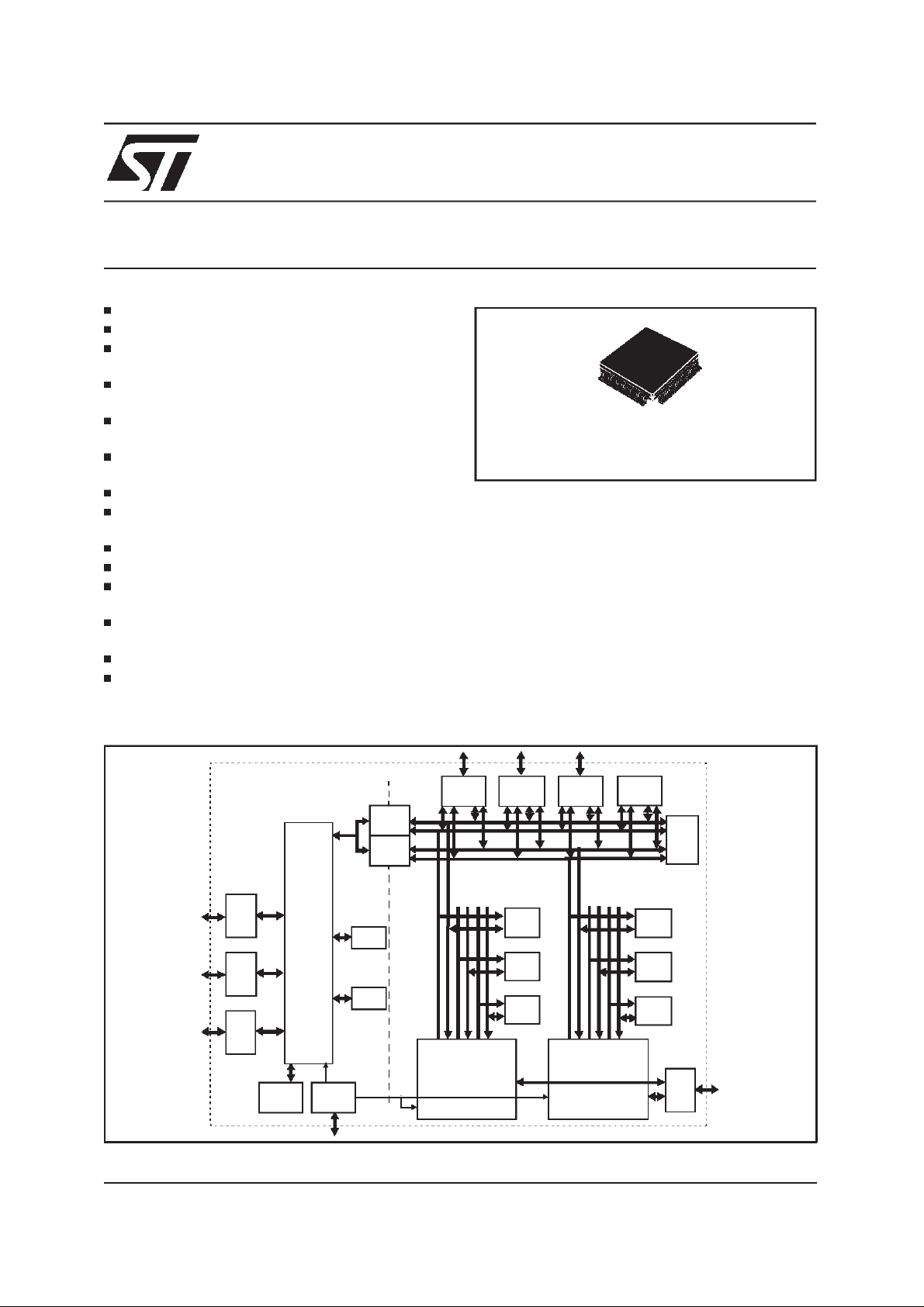
BLOCK DIAGRAM
TDA7503
PRODUCT PREVIEW
TQFP100
DESCRIPTION
The device is a high-performance Digital Signal
ProcessingIC particularly suitedto Audio applications. The device contains two 24-bit 40 MIPS
DSP cores delivering a total of 80 MIPS of DSP
processing power. There is also an embedded 8bit Microcontrollerto handle all control functions.
All data and program memories for both DSP
cores are on-chip. A variety of highly programmable and flexible peripheral blocks for both the Microcontroller and the DSPs have been integrated
to form a powerful audio processing system on a
single chip.
Host
Interface 0
Host
Interface1
Serial
Audio
Interface
XDB0
XAB0
XDB1
XAB1
Synchronous
Audio
Interface
SRAM/
DRAM
Interface
XCHG
Interface
Cordic
Arithmetic
Unit
M8051
CORE
Control
Interface
Interface
Peripheral
Micro
Memory
Interface
Serial
Watchdog
Timer
MCLK
PLL
Clock
Oscillator
AUX-RAM
768 Bytes
AUX-RAM
256 Bytes
DCLK
YAB0
XDB0
XAB0
DSP0
CORE
YDB0
PAB0
PDB0
X-RAM0
X-ROM0
Y-RAM0
Y-ROM0
P-RAM0
P-ROM0
XDB1
XAB1
DSP1
CORE
YAB1
YDB1
PAB1
PDB1
X-RAM1
X-ROM1
Y-RAM1
Y-ROM1
P-RAM1
P-ROM1
DEBUG
Interface
July 1999
This is preliminaryinformation on a new product now in development. Details are subject to change without notice.
1/26
TDA7503
ABSOLUTE MAXIMUM RATINGS
Symbol Parameter Value Unit
V
DDC
V
DDP
V
I,VIN
T
op
T
stg
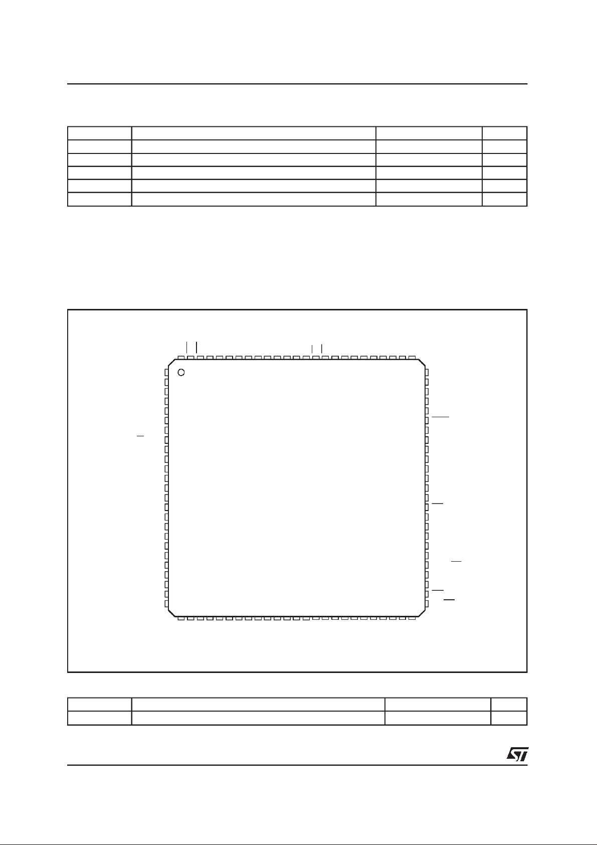
PIN CONNECTION
Core DC Supply voltage -0.5 to 5 V
Pads DC Supply voltage -0.5 to 6.5 V
Digital or analog input voltage -0.5 to (V
+0.5) V
DDP
Operative temperature range -40 to 85 °C
Storage temperature range(plastic) -55 to 150 °C
RD(P3.7)
WR(P3.6)
xALE
RAD0(P0.0)
RAD2(P0.2)
RAD1(P0.1)
RAD3(P0.3)
RAD4(P0.4)
RAD5(P0.5)
RAD6(P0.6)
RAD7(P0.7)
RA10(P2.2)
75
VSSI3_CORE4
74
VDDI3_CORE4
73
VSSE5_MI1
72
VDDE5_MI1
71
70
XPSEN
69
RA11(P2.3)
68
RA9(P2.1)
RA8(P2.0)
67
RA13(P2.5)
66
RA14(P2.6)
65
64
RA15(P2.7)
63
RA12(P2.4)
62
SRA10/DRA6
61
DRD
60
SRA11/DRA7
59
SRA9/DRA5
58
VDDE5_DR2
57
VSSE5_DR2
56
SRA8/DRA4
55
SRA13/RAS
54
VSSI3_CORE1
53
VDDI3_CORE1
52
DWR
51
ALE/CAS
T1(P3.5)
VDDI3_CORE3
VSSI3_CORE3
RESET
MISO
MOSI
SCLK
SS/GPIOS
VSSE5_CI1
VDDE5_CI1
LRCKR
SCLKR
SDI3
SDI2
SDI1
SDI0
SDO4
SDO3
SDO2
SDO1
SDO0
VSSI3_CORE2
VDDI3_CORE2
SCLKT
LRCKT
T0(P3.4)
100 99 98
1
2
3
4
5
6
7
8
9
10
12
13
14
15
16
17
18
19
20
21
22
23
24
25
26 27 28
TXD(P3.1)
RXD(P3.0)
GPIO6(P1.6)
GPIO5(P1.5)
GPIO3(P1.3)
GPIO4(P1.4)
INT0(P3.2)
INT1(P3.3)
97 96 95 94 9293 91 90 89 88 87
29 30 31 32 33
VDDE5_MI2
34 35 36 37 38 39
VSSE5_MI2
GPIO2(P1.2)
GPIO1(P1.1)
GPIO0(P1.0)
86 85 84 83 8182 80 79 78 77 76
40 41 42 43 44
451146 47 48 49 50
XTI
FILT
XTO
VSSE5_SA1
VDDE5_SA1
PGND
PVCC
TESTEN
SCANEN
DBOUT
DBCK/OS1
DBRQN
DBIN/OS0
DBSEL
SRA_D7/DRA3
VDDE5_DR1
SRA_D6/DRA2
SRA_D5/DRA1
SRA_D4/DRA0
VSSE5_DR1
SRA_D3/DRD3
SRA_D2/DRD2
SRA12/DRA8
SRA_D1/DRD1
SRA_D0/DRD0
D97AU693
THERMAL DATA
Symbol Parameter Value Unit
Thermal resistance Junction to Ambient 85 °C/W
2/26
R
th j-amb
PIN DESCRIPTION
TDA7503
N. Name Type
11 LRCKR I – Audio Serial Port Receive Left/Right Frame Sync. The Left/Right select
12 SCLKR I – Audio Serial Port Receive Bit Clock. SCLK clocks receiveddigital audio
16 SDI0 I – StereoDigitalAudioData.SDI0is a stereodigital audiodatainput pin
15 SDI1 I – StereoDigitalAudioData.SDI1is a stereodigital audiodatainput pin
14 SDI2 I – StereoDigitalAudioData.SDI2is a stereodigital audiodatainput pin
13 SDI3 I – Stereo Digital Audio Data / Serial Receive Data. SDI3 is a stereo digital
25 LRCKT I – Audio Serial Port Transmit Left/Right Frame Sync /Frame Sync. The
24 SCLKT I – Audio Serial Port Transmit Bit Clock/SSI SerialBit Clock. SCLK clocks
21 SDO0 O High StereoDigitalAudio Data. SDO0is a stereodigitalaudiodataoutput pin
20 SDO1 O High StereoDigitalAudio Data. SDO1is a stereodigitalaudiodataoutput pin
19 SDO2 O High StereoDigitalAudio Data. SDO2is a stereodigitalaudiodataoutput pin
18 SDO3 O High StereoDigitalAudio Data. SDO3is a stereodigitalaudiodataoutput pin
17 SDO4 O High Stereo Digital Audio Data /Serial Transmit Data. SDO4 is a stereo digital
34 SCANEN I – SCAN Enable.Enable SCAN Path andMUXingofSCANINand SCANOUT
33 TESTEN I – Test Enable. Enable Scan Mode Clocks. An active low signal will enable
49 SRA_D0/DRD0 I/O I DSP SRAM Multiplexed Address/Data Line 0/DSP DRAM Data Line
48 SRA_D1/DRD1 I/O I DSP SRAM Multiplexed Address/Data Line 1/DSP DRAM Data Line
47 SRA_D2/DRD2 I/O I DSP SRAM Multiplexed Address/Data Line 2/DSP DRAM Data Line
46 SRA_D3/DRD3 I/O I DSP SRAM Multiplexed Address/Data Line 3/DSP DRAM Data Line
43 SRA_D4/DRA0 I/O O, High DSP SRAM Multiplexed Address/Data Line 4/DSP DRAM Address Line
Reset
Status (1)
Function
signal for received serial audiodata. This signal has a frequency equal to
the audio sample rate.
data into pins SDI0, SDI1, SDI2, and SDI3
channel 0.
channel 1.
channel 2.
audio data input pinand is multiplexed with the SSI’s Serial Receive
Data Input channel 3.
Left/Right select signal for transmittedserial audio data. This signal has a
frequency equal to the audio sample rate. This signal is multiplexed with
the SSI’s Frame Sync Input.
digital audio data out of pinsSDO0, SDO1, SD02, SD03, and SD04. This
pin is multiplexed with the SSI’s serial bitclock.
channel0.
channel1.
channel2.
channel3.
audio data output pin and is multiplexed with the SSI’s Serial Transmit
Data Output channel4.
Pins.
the same clock to all scan chains. This pin also makes all latches
transparent.
0.When in SRAM Mode these pins act as the EMI multiplexed address
and data line 0. When in DRAM Mode they act as the EMI data line 0.
1.When in SRAM Mode these pins act as the EMI multiplexed address
and data line 1. When in DRAM Mode they act as the EMI data line 1.
2.When in SRAM Mode these pins act as the EMI multiplexed address
and data line 2. When in DRAM Mode they act as the EMI data line 2.
3.When in SRAM Mode these pins act as the EMI multiplexed address
and data line 3. When in DRAM Mode they act as the EMI data line 3.
0. When in SRAM Mode these pins act as theEMI multiplexed address
and data line 4. When in DRAM Mode they act as the EMI address line 0.
3/26
TDA7503
PIN DESCRIPTION
N. Name Type
42 SRA_D5/DRA1 I/O O, High DSP SRAM Multiplexed Address/Data Line 5/DSP DRAM Address Line
41 SRA_D6/DRA2 I/O O, High DSP SRAM Multiplexed Address/Data Line 6/DSP DRAM Address Line
40 SRA_D7/DRA3 I/O O, High DSP SRAM Multiplexed Address/Data Line 7/DSP DRAM Address Line
56 SRA8/DRA4 O High DSP SRAM Address Line 8/DSP DRAM Address Line 4. When in SRAM
59 SRA9/DRA5 O High DSP SRAM Address Line 9/DSP DRAM Address Line 5. When in SRAM
62 SRA10/DRA6 O High DSP SRAM Address Line 10/DSP DRAM Address Line 6. When in
60 SRA11/DRA7 O High DSP SRAM Address Line 11/DSP DRAM Address Line 7. When in
50 SRA12/DRA8 O High DSP SRAM Address Line 12/DSP DRAM Address Line 8. When in
55 SRA13/RAS O High DSP SRAM Address Line 13/DRAM Row Address Strobe. When in
51 ALE/CAS O High DSP SRAM Address latch enable/colomn Address. When in SRAM
52 DWR O High DSP SRAM Write Enable/DRAM WriteEnable. This pin serves as the
61 DRD O High DSP SRAM Read Enable/DRAM Read Enable. This pinserves as the
36 DBCK/OS1 I/O I Debug Port Bit Clock/Chip Status 1. The serial clock for the Debug Port
37 DBIN/OS0 I/O I Debug Port Serial Input/Chip Status 0. The serial data input for the
35 DBOUT I/O I Debug Port Serial Output. The serial data output for the Debug Port. Can
38 DBRQN I – Debug Port Request Input. Means of entering the Debug mode of
39 DBSEL I – Debug Port MUX Selection. Selects either DSP0 or DSP1 to be
67 RA8(P2.0) I/O I Microcontroller High Byte Address Lines.This pin is the address line 8 of
68 RA9(P2.1) I/O I Microcontroller High Byte Address Lines.This pin is the address line 9 of
(continued)
Status (1)
Reset
Function
1. When in SRAM Mode these pins act as theEMI multiplexed address
and data line 5. When in DRAM Mode they act as the EMI address line 1.
2. When in SRAM Mode these pins act as theEMI multiplexed address
and data line 6. When in DRAM Mode they act as the EMI address line 2.
3. When in SRAM Mode these pins act as theEMI multiplexed address
and data line 7. When in DRAM Mode they act as the EMI address line 3.
Mode these pins act as the EMI address line 8.When in DRAM Mode
they act as the EMI address line 4.
Mode these pins act as the EMI address line 9.When in DRAM Mode
they act as the EMI address line 5.
SRAM Mode these pins act as the EMI address line 10.When in DRAM
Mode they act as the EMI address line 6.
SRAM Mode these pins act as the EMI address line 11. When in DRAM
Mode they act as the EMI address line 7.
SRAM Mode these pins act as the EMI address line 12. When in DRAM
Mode they act as the EMI address line 8.
SRAM Mode this pin acts as the EMI address lines 13. When in DRAM
Mode this pin acts as the row address strobe.
Mode this pin acts as the EMI Address Latch Enable. When in DRAM
Mode this pin acts as the column address strobe.
write enable for the EMI when in DRAM and SRAM Modes.
read enable for the EMI when in DRAM and SRAM Modes.
is provided when an input. When an output, together with OS0 provides
information about the chip status. Can also be used as GPIO for the
8051.
Debug Port is provided when an input. When an output, together with
OS1 provides information about the chip status. Can also be used as
GPIO for the 8051.
also be used as a GPIO for the 8051.
operation.
connected to the Debug Port pins.
a 16 bit address, for external EPROM and memory mapped devices. It
can also actas GPIO using the P2 and P2DIR registers.
a 16 bit address, for external EPROM and memory mapped devices. It
can also actas GPIO using the P2 and P2DIR registers.
4/26
TDA7503
PIN DESCRIPTION
N. Name Type
75 RA10(P2.2) I/O I Microcontroller High Byte Address Lines. This pin is the address line 10
69 RA11(P2.3) I/O I Microcontroller High Byte Address Lines. This pin is the address line 11
63 RA12(P2.4) I/O I Microcontroller High Byte Address Lines. This pin is the address line 12
66 RA13(P2.5) I/O I Microcontroller High Byte Address Lines. This pin is the address line 13
65 RA14(P2.6) I/O I Microcontroller High Byte Address Lines. This pin is the address line 14
64 RA15(P2.7) I/O I Microcontroller High Byte Address Lines. This pin is the address line 15
83 RAD0(P0.0) I/O I Microcontroller Address/Data Pins. This pin is the multiplexed address
82 RAD1(P0.1) I/O I Microcontroller Address/Data Pins. This pin is the multiplexed address
81 RAD2(P0.2) I/O I Microcontroller Address/Data Pins. This pin is the multiplexed address
80 RAD3(P0.3) I/O I Microcontroller Address/Data Pins. This pin is the multiplexed address
79 RAD4(P0.4) I/O I Microcontroller Address/Data Pins. This pin is the multiplexed address
78 RAD5(P0.5) I/O I Microcontroller Address/Data Pins. This pin is the multiplexed address
77 RAD6(P0.6) I/O I Microcontroller Address/Data Pins. This pin is the multiplexed address
76 RAD7(P0.7) I/O I Microcontroller Address/Data Pins. This pin is the multiplexed address
84 xALE I/O I Microcontroller External Address Latch Enable. This pin is the address
85 WR(P3.6) I/O I Microcontroller Write Strobe. External data memory write strobe. This pin
86 RD(P3.7) I/O I Microcontroller Read Strobe. External data memory readstrobe. Active
70 XPSEN I/O I Microcontroller External Program Memory Enable. External program
(continued)
Status (1)
Reset
Function
of a 16 bit address, for external EPROM and memory mapped devices. It
can also actas GPIO using the P2 and P2DIR registers.
of a 16 bit address, for external EPROM and memory mapped devices. It
can also actas GPIO using the P2 and P2DIR registers.
of a 16 bit address, for external EPROM and memory mapped devices. It
can also actas GPIO using the P2 and P2DIR registers.
of a 16 bit address, for external EPROM and memory mapped devices. It
can also actas GPIO using the P2 and P2DIR registers.
of a 16 bit address, for external EPROM and memory mapped devices. It
can also actas GPIO using the P2 and P2DIR registers.
of a 16 bit address, for external EPROM and memory mapped devices. It
can also actas GPIO using the P2 and P2DIR registers.
and data line bit 0 for external EPROM and memory mapped peripherals.
It can also actas GPIO using the P0 and P0DIR registers.
and data line bit 1 for external EPROM and memory mapped peripherals.
It can also actas GPIO using the P0 and P0DIR registers.
and data line bit 2 for external EPROM and memory mapped peripherals.
It can also actas GPIO using the P0 and P0DIR registers.
and data line bit 3 for external EPROM and memory mapped peripherals.
It can also actas GPIO using the P0 and P0DIR registers.
and data line bit 4 for external EPROM and memory mapped peripherals.
It can also actas GPIO using the P0 and P0DIR registers.
and data line bit 5 for external EPROM and memory mapped peripherals.
It can also actas GPIO using the P0 and P0DIR registers.
and data line bit 6 for external EPROM and memory mapped peripherals.
It can also actas GPIO using the P0 and P0DIR registers.
and data line bit 7 for external EPROM and memory mapped peripherals.
It can also actas GPIO using the P0 and P0DIR registers.
latch enable. A logic high indicates that address/data lines 7 through 0
represent an address. Inactive for Program/Data fetches from internal
AUX.
can also actas GPIO using the P3 and P3DIR registers.
Low, or GPIO. Thispin can also act as GPIO using the P3 and P3DIR
registers. Disabled by setting the RDSEL bit in the PINCTL register.
memory enable pin. Active Low. Changes functionality to RD when
Microcontroller is fetching instructions out of internal AUX ram.
Controlled by the PSSEL and PSBIT bits in the PINCTL register.
5/26
TDA7503
PIN DESCRIPTION
N. Name Type
4 RESET I/O I System Reset. A logic low level applied to RESET input initializes the
96 RXD(P3.0) I/O I Microcontroller Standard Serial Interface (Asynchronous) Input Data. Or
97 TXD(P3.1) I/O I Microcontroller Standard Serial Interface (Asynchronous) Output Data.
99 INT0(P3.2) I/O I Microcontroller Interrupt 0. When pulled low, INT0 asserts a
98 INT1(P3.3) I/O I Microcontroller Interrupt 1. When pulled low, INT1 asserts a
100 T0(P3.4) I/O I Microcontroller Timer 0 External Input. Input event clock for timer 0, or
1 T1(P3.5) I/O I Microcontroller Timer 1 External Input. Input event clock for timer 1, or
87 GPIO0(P1.0) I/O I Microcontroller General Purpose. This GPIO linecan be configured to be
88 GPIO1(P1.1) I/O I Microcontroller General Purpose. This GPIO linecan be configured to be
89 GPIO2(P1.2) I/O I Microcontroller General Purpose. This GPIO linecan be configured to be
92 GPIO3(P1.3) I/O I Microcontroller General Purpose. This GPIO linecan be configured to be
93 GPIO4(P1.4) I/O I Microcontroller General Purpose. This GPIO linecan be configured to be
94 GPIO5(P1.5) I/O I Microcontroller General Purpose. This GPIO linecan be configured to be
95 GPIO6(P1.6) I/O I Microcontroller General Purpose. This GPIO linecan be configured to be
7 SCLK I/O I Microcontroller General Purpose. Each of the six GPIO lines canbe
6 MOSI I/O I Microcontroller SPI Master Output Slave Input Serial Data . Serial Data
(continued)
Status (1)
Reset
Function
microcontroller. The micro is responsible for initializing the DSPs. If the
watchdog timer overflow occurs this pin is driven low for 1 watchdog
timer cycle. During Debug Mode if this pin is pulled low in while the
DBRQN line is pulled low then the DSP pointed to by the DBSEL pin will
be reset.
GPIO. This pin can also act as GPIO using the P3 and P3DIR registers.
Or GPIO. This pin can also act as GPIO using the P3 and P3DIR
registers.
microcontroller external interrupt. In addition,if this pin is pulled low
during powerdown this allowsthe M8051 to resume executing intructions
where it left off. This pin can also act as GPIO using the P3 and P3DIR
registers.
microcontroller external interrupt. In addition,if this pin is pulled low
during powerdown this allowsthe M8051 to resume executing intructions
where it left off. This pin can also act as GPIO using the P3 and P3DIR
registers.
GPIO. This pin can also act as GPIO using the P3 and P3DIR registers.
GPIO. This pin can also act as GPIO using the P3 and P3DIR registers.
digital input or output bywriting to the P1 and P1DIR registers.This pin is
tri-stated while the RESET pin is held low and is pulled low when RESET
is released. This pin will be pulled high when in IDLE or PWRDN modes.
digital input or output bywriting to the P1 and P1DIR registers. At reset it
is configured as an input with the output tri-stated.
digital input or output bywriting to the P1 and P1DIR registers. At reset it
is configured as an input with the output tri-stated.
digital input or output bywriting to the P1 and P1DIR registers. At reset it
is configured as an input with the output tri-stated.
digital input or output bywriting to the P1 and P1DIR registers. At reset it
is configured as an input with the output tri-stated.
digital input or output bywriting to the P1 and P1DIR registers. At reset it
is configured as an input with the output tri-stated.
digital input or output bywriting to the P1 and P1DIR registers. At reset it
is configured as an input with the output tri-stated.
individually configured to be digitalinput oroutput by writing to the P1
and P1DIR registers. All GPIOs are configured to be inputs with the
outputs tri-stated except for P1.0. This pin is tri-stated during while the
RESET pin is held low and is pulled low when RESET is released. This
pin will be pulled high whenin IDLE or PWRDN modes.
Output for SPI type serial port when in SPI Master Mode andSerial Data
Input when in SPI Slave Mode.
6/26
TDA7503
PIN DESCRIPTION
N. Name Type
5 MISO I/O I Microcontroller SPI Master Input Slave Output Serial Data . Serial Data
8 SS/GPIOS I/O I Microcontroller SPI Slave Select . Slave Select Input for SPI type serial
32 PVCC I – PLL Clock Power Supply . Vdd Pin for PLL Clock Oscillator.
28 XTO O High Crystal Oscillator Output. Crystal Oscillator output drive.
29 XTI I – Crystal Oscillator Input. External Clock Input or crystal connection.
30 FILT O High PLL Loop Filter Capacitor Output. Capacitor connected between FILT
31 PGND I – PLL Clock GroundInput. Ground connection for oscillator circuit.
53 VDDI3_CORE1 PWR – 3.3V core supply.
23 VDDI3_CORE2 PWR – 3.3V core supply.
2 VDDI3_CORE3 PWR – 3.3V core supply.
73 VDDI3_CORE4 PWR – 3.3V core supply.
54 VSSI3_CORE1 GND – Core ground.
22 VSSI3_CORE2 GND – Core ground.
3 VSSI3_CORE3 GND – Core ground.
74 VSSI3_CORE4 GND – Core ground.
27 VDDE5_SA1 PWR – 5V supply for SAI pads.
26 VSSE5_SA1 GND – Ground for SAI pads.
10 VDDE5_CI1 PWR – 5V supply for Control Interface Pads.
9 VSSE5_CI1 GND – Ground forControl Interface Pads.
71 VDDE5_MI1 PWR – 5V supply for Micro Memory Interface Pads.
91 VDDE5_MI2 PWR – 5V supply for Micro Memory Interface Pads.
72 VSSE5_MI1 GND – Ground forMicro Memory Interface Pads.
90 VSSE5_MI2 GND – Ground forMicro Memory Interface Pads.
44 VDDE5_DR1 PWR – 5V supply for DSP EMI Interface Pads.
58 VDDE5_DR2 PWR – 5V supply for DSP EMI Interface Pads.
45 VSSE5_DR1 GND – Ground for DSP EMI Interface Pads.
57 VSSE5_DR2 GND – Ground for DSP EMI Interface Pads.
(continued)
Status (1)
Reset
Function
Input for SPI style serial port when in SPI Master Mode and Serial Data
Output when in SPI Slave Mode.
port. This pin can be used as a GPIO when the SPI is disabled or in
master mode.
and XGND establishes primary PLL.
7/26
TDA7503
RECOMMENDED DC OPERATING CONDITIONS
Symbol Parameter Test Condition Min. Typ. Max. Unit
V
DDC
DDP 5V Power Supply Voltage 4.5 5 5.5 V
V
Tj Operating Junction
GENERAL INTERFACE ELECTRICALCHARACTERISTICS
Symbol Parameter Test Condition Min. Typ. Max. Unit Note
I
il
I
ih
I
oz
C
in
I
latchup
V
esd
Note 1: Theleakage currents are generally very small, < 1nA. The value given here, 1mA, is a maximum that can occur after an Electrostatic
Stress on the pin.
Note 2: Guaranteedby design.
Note 3: Human Body Model.
3.3V Power Supply Voltage 3 3.3 3.6 V
-40 125 °C
Temperature
Low Level Input Current
Vi=0V 1 µA1
Without pull-up device
High Level Input Current
Vi = V
DDP
1 µA1
Without pull-down device
Tri-state Output leakage
Vo = 0V or V
DDP
1 µA1
Without pullup/down device
Input capacitance 10 pF 2
I/O Latch-up Current V < 0V, V > V
DDP
200 mA
Electrostatic Protection Leakage < 1µA 2000 V 3
DC ELECTRICAL CHARACTERISTICS
Symbol Parameter Test Condition Min. Typ. Max. Unit Note
V
il
V
ih
V
ol
V
oh
Note 1: Takes intoaccount 200mV voltage drop in both supply lines.
Low Level Input Voltage 0.25⋅V
High Level Input Voltage 0.7⋅V
Low Level Output Voltage Iol= 2mA 0.4 V 1
High Level Output Voltage Iol= -2mA V
8/26
DDP
DDP
-0.4 V 1
DDP
V
V

TDA7503
POWERCONSUMPTION
Symbol Parameter Value Unit
P
tot
Note: 40MHz internalDSP clock at Tamb
EXTERNAL CLOCKS (XTI Pin)
The TDA7503 systemclock is externallysupplied via the XTI pin.
Timingsshown in thisdocument are valid for clock rise and fall timesof 3ns maximum.
Symbol Characteristics Value Unit
F
ext
When PLL isenabled see constraints for InternalClocks.
INTERNAL CLOCKS
Symbol Characteristics Expression
f
DSP_MAX
f
µP_MAX
f
DSP
f
µ
P
I
cyc_DSP
I
cyc_µP
Note 1: If the DCKSRC bit of the clock control register is 0 then dclk = Fext/2.
Note 2
:If the MCKSRC bit of the clock control register is 1 then mclk = Fext else of MCKSRC0 is 0 then MCLK = Fext/4.
Note 3: DF is PLL input devide factor, bits IDF [4:0]of PLL control register one.
Note 4
:MF is PLL multiply devide factor, bits MP [6:0] of PLL control register zero.
Maximum current for core power supply @ 3.3V 320 mA
Max. Frequency @ XTI when PLL is disabled 20 MHz
Maximum DSP Internal Operation Frequency (dclk) 40MHz
Maximum µP (8051)Internal Operation Frequency (mclk) 20MHz
Internal DSP Clock Cycle Frequency (dclk)
MF ⋅ F
ext
2⋅DF
InernalµP (8051) Clock Cycle Frequency (mclk)
MF⋅F
ext
4⋅ DF
DSP Machine Cycle Time dclk
µP (8051) Machine Cycle Time mclk/12
PHASE LOCKED LOOP (PLL) CHARACTERISTICS
Characteristics Expression Value Unit
VCO frequency when PLL enabled
MF ⋅ Fext
40 to 80 MHz
DF
Recommended PLL external capacitor (pin
3.3 nF
FILT)
RESET
Characteristics Expression Unit
Minimum RESET assertion 100/Fext ns
9/26

TDA7503
SAI/SSIINTERFACE
Figure 1. SAI and SSI Timings
SDI0-3
LRCKR
SCKR
(RCKP=0)
t
sckpl
t
dt
t
t
sdis
Valid
Valid
t
lrh
t
sckph
t
t
sdih
sckr
lrs
Timing Description Value Unit
Note T
t
t
t
t
sckph
t
sckpl
DSP
sckr
t
dt
t
lrs
t
lrh
sdid
sdih
Minimum Clock Cycle 3T
SCKR active edge to data out valid 40 ns
LRCK setup time 5 ns
LRCK hold time 5 ns
SDI setup time 5 ns
SDI hold time 5 ns
Minimum SCK high time 0.35 t
Minimum SCK low time 0.35 t
= dsp master clock cycle time= 1/F
DSP
+5 ns
DSP
sckr
sckr
ns
ns
Figure 2. SAI Interrupt protocol
LRCKT
TDE
LRCKR
RDR
10/26
Left Right Left Right
Internal Flag set when left data written
to all enabled transmitters. If this internal
flag is set then right data must written
to data registers before the next
falling edge of LRCKT.
Left Right Left Right
TDE cleared when right data written
to all enabled transmitters.
RDR cleared when right data read from
all enabled transmitters.
Internal Flag set when left data read
from all enabled receivers. If this internal
flag is set then right data must read
from data registers before the next
rising edge of LRCKR.

Figure 3. SAI protocol when RLRS=0; RREL=0; RCKP=1; RDIR=0.
TDA7503
LRCKR
LEFT
RIGHT
SCKR
LSB(n-1) MSB(word n)
MSB-1 (n)
SDI0
Figure 4. SAI protocol when RLRS=1; RREL=0; RCKP=1; RDIR=1.
LRCKR
SCKR
SDI0
LEFT
MSB(n-1) LSB(wordn)
RIGHT
LSB+1(n)
LSB+2 (n)
Figure 5. SAI protocol when RLRS=0; RREL=0; RCKP=0; RDIR=0.
MSB-2 (n)
LRCKR
SCKR
SDI0
LEFT
LSB(n-1) MSB(word n)
RIGHT
MSB-1 (n)
Figure 6. SAI protocol when RLRS=0; RREL=1; RCKP=1; RDIR=0.
RIGHT
MSB-1 (n)
MSB-2 (n)
LRCKR
SCKR
SDI0
LEFT
LSB(n-1)
MSB(word n)
MSB-2 (n)
11/26

TDA7503
Figure 7. SSI Protocol.
FrameSync 0
FrameSync 1
NETWORK MODE
FiveWord Packet
Data In
SCK
Receive
Interrupts
FrameSync 0
FrameSync 1
Data In
SCK
Receive
Interrupts
DataWord
NORMALMODE
The timing diagrams for the SSI Interface are
shown in Figure 7 for both Network and Normal
modes.
In NormalMode the rising edge FSYNC starts the
internal bit counter to allow data to be clocked in
or out. When bit count is equal to the programmed word length the counter is reset and
the shift register is broadside loaded into the data
register. Additional SCK pulses are ignored after
the counter is reset. The next word is clocked in
or out starting with the next rising edge of
FSYNC.
12/26
In Network Mode the rising edge FSYNC starts
the internal bit counter to allow data to be clocked
in or out. When bit count is equal to the programmed word length the counter is reset and
the shift register is broadside loaded into the data
register. At this point the FSRSD bit is set indicating that a frame sync was received with that
word. After being reset the counter continues
counting, clocking in the next word. Only when
the next rising edge of FSYNC is detected is the
packet consideredcomplete.

SPI INTERFACE
TDA7503
Symbol Description
t
sclk
t
t
t
sclk
t
t
t
sckph
t
sckpl
Clock Cycle mclk/12
Sclk edge to MOSI valid 40
dtr
MISO setup time 5
dts
Clock Cycle mclk/6 µs
Sclk edge to MOSI valid 40 µs
dtr
MISO setup time 5 µs
dts
Minimum SCK high time mclk/12 µs
Minimum SCK low time mclk/12 µs
Figure 8. SPI Clocking scheme.
SS
SCLK
SCLK
SCLK
(CPOL=0, CPHA=0)
(CPOL=0, CPHA=1)
(CPOL=1, CPHA=0)
MASTER
SLAVE
Min
Value
Unit
µ
µ
µ
s
s
s
SCLK
MISO/
MOSI
(CPOL=1, CPHA=1)
MSB 6 5 4 3 2 1 LSB
Internal Strobe for Data Capture
13/26

TDA7503
MICRO MEMORYINTERFACE
Figure 9. Timing diagram for External Memory Interface
For the calculationof slowest access timeallowed for a memoryattached to the M8051, the
followingdiagram illustrates the timing constraints.Slowest access time allowed, t
4*mclk- t
setuptime, t
, wherethe worst case addressdelay, tad= 30 ns, and the worst case data
ad-tds
= 20 ns.
ds
mclk
XALE
XPSEN
OPLOAD
Address
Data
acc
=
t
ad
GENERAL PURPOSE I/O (GPIO) INTERFACE
Timing Characteristics
XTI Edge to GPIO Out Valid (GPIO Out Delay Time) -- 26 ns
t
god
XTI Edge to GPIO Out Not Valid (GPIO Out Hold Time) 2 -- ns
t
goh
GPIO In Valid to XTI Edge (GPIO In Set-up Time) 10 -- ns
t
gis
XTI Edge to GPIO In Not Valid (GPIO In Hold Time) 6 -- ns
t
gih
Figure 10. GPIOTiming
t
acc
t
ds
mclk = 20MHz
Min. Max.
Unit
14/26

Debug Port Interface
TDA7503
No. Characteristics
dclk = 40MHz
Min. Max.
Unit
1 DBCK rise time -- 3 ns
2 DBCK fall time -- 3 ns
3 DBCK Low 40 -- ns
4 DBCK High 40 -- ns
5 DBCK Cycle Time 200 -- ns
6 DBRQN Asserted to DBOUT (ACK) Asserted 5 T
DSP
-- ns
7 DBCK High to DBOUT Valid -- 42 ns
8 DBCK High to DBOUT Invalid 3 -- ns
9 DBIN Valid to DBCK Low (Set-up) 15 -- ns
10 DBCK Low to DBIN Invalid (Hold) 3 -- ns
DBOUT (ACK) Asserted to First DBCK High 2 Tc -- ns
DBOUT (ACK) Assertion Width 4.5 T
11 Last DBCK Low of Read Registerto First DBCK High of Next
-3 5T
DSP
+10 -- ns
7T
DSP
+7 ns
DSP
Command
12 Last DBCK Low to DBOUT Invalid (Hold) 3 -- ns
DBSEL setup to DBCK T
DSP
ns
15/26

TDA7503
Figure 11. Debug Port Serial Clock Timing.
Figure 12. Debug Port AcknowledgeTiming.
Figure 13. Debug Port Data I/O to StatusTiming.
Figure 14. Debug Port Read Timing.
Figure 15. Debug Port DBCK Next Command After Read Register Timing.
16/26

EXTERNAL MEMORY INTERFACE(EMI) DRAM MODE
TDA7503
Characteristics
Page Mode Cycle Time slow
RAS or RD Assertion to Data Valid slow
CAS Assertion to Data Valid slow
Column Address Valid to Data Valid slow
CAS Assertion to Data Active 0 -- ns
RAS Assertion Pulse Width (Note 1)
(Page Mode Access Only)
RAS Assertion Pulse Width (Single Access Only) slow
RAS or CAS Negation to RAS Assertion slow
CAS Assertion Pulse Width slow
Last CAS Assertion to RAS Negation (Page Mode Access Only) slow
Note: 1. n is the number of successive accesses. n = 2,3, 4, or 6.
Timing
Mode
fast
fast
fast
fast
slow
fast
fast
fast
fast
fast
40MHz
Min. Max.
100
75
--
--
--
--
--
--
264
189
164
114
120
70
65
40
60
35
--
--
159
109
65
40
80
55
--
--
--
--
--
--
--
--
--
--
Unit
ns
ns
ns
ns
ns
ns
ns
ns
ns
ns
ns
ns
ns
ns
ns
ns
ns
ns
DRAM Refresh Timing
Characteristics
RAS Negation to RAS Assertion slow
CAS Negation to CAS Assertion slow
Refresh Cycle Time slow
RAS Assertion Pulse Width slow
RAS Negation to RAS Assertion for Refresh Cycle (Note 1) slow
CAS Assertion to RAS Assertion on Refresh Cycle 18 -- ns
RAS Assertion to CAS Negation on Refresh Cycle slow
RAS Negation to CAS Assertion on a Refresh Cycle slow
CAS Negation to Data Not Valid 0 -- ns
Note: 1. Happens when a Refresh Cycle is followed by an Access Cycle.
Timing
Mode
fast
fast
fast
fast
fast
fast
fast
40MHz
Min. Max.
143
93
118
68
325
225
166
116
120
70
160
110
114
64
--
--
--
--
--
--
--
--
--
--
--
--
--
--
Unit
ns
ns
ns
ns
ns
ns
ns
ns
ns
ns
ns
ns
ns
ns
17/26

TDA7503
EXTERNAL MEMORY INTERFACE(EMI) SRAM MODE
Characteristics
Address Valid and CS Assertion Pulse Width 89 -- ns
Address Valid to RD or WR Assertion 23 -- ns
RD or WR Assertion Pulse Width 45 -- ns
RD or WR Negation to RD or WR Assertion 39 -- ns
RD or WR Negation to Address not Valid 5 -- ns
Address Valid to Input Data Valid -- 72 ns
RD Assertion to Input Data Valid -- 35 ns
RD Negation to Data Not Valid (Data Hold Time) 0 -- ns
Address Valid to WR Negation 73 -- ns
Data Setup Time to WR Negation 32 -- ns
Data Hold Time from WR Negation 5 -- ns
WR Assertion to Data Valid -- 18 ns
WR Negation to Data High-Z (Note 1) -- 23 ns
WR Assertion to Data Active 5 -- ns
40MHz
Min. Max.
Unit
18/26

Figure 16. External Memory Interface SRAM Read Cycle.
TDA7503
SRA_D
[7:0]
SRA_D
[13:8]
ALE
DRD
add. [7:0]
add. [13:8]
Figure 17. External Memory Interface SRAM WriteCycle.
SRA
[7:0]
SRA
[13:8]
add. [7:0]
add. [13:8]
data
data
ALE
DWR
Figure 18. DRAM Read Cycle.
DRA[8:0]
RAS
CAS
DRD
DRD [3:0]
Row address 1 Column address 1
Column address 2 Row address 2
nibble 1 nibble 2
19/26

TDA7503
Figure 19. DRAM Write Cycle.
DRA [8:0]
RAS
CAS
DWR
DRD[3:0]
Row address 1
Column address 1 Column address 2 Row address 2
nibble 1
FUNCTIONAL DESCRIPTION.
The Aladdin IC broken up into two distinct blocks.
One block contains the two DSP Cores and their
associated peripherals. The other contains the
M8051 Core and its associated peripherals. The
interface between the two blocks is the Host Interface.
24-BIT DSP CORE.
The two DSP cores are used to process the con-
verted analog audio data coming from the
CODEC chip via the SAI and return it for analog
conversion. Functions such as volume, tone, balance, and fader control, as well as spatial enhancement and general purpose signal processing maybe performedby the DSPs.
Some capabilitiesof the DSPs are listed below:
Single cycle multiply and accumulate with convergent rounding and condition code generation
2 x 56-bitAccumulators
Doubleprecision multiply
Scaling and saturation arithmetic
48-bitor 2 x 24-bit parallelmoves
64 interruptvector locations
Fastor long interrupts possible
Programmableinterrupt prioritiesand masking
8 each of Address Registers, Address Offset
Registersand Address ModuloRegisters
Linear, Reverse Carry, Multiple Buffer Modulo,
Multiple Wrap-around Modulo address arithmetic
Post-incrementor decrement by 1 or by offset,
Index by offset,predecrementaddress
nibble 2
Repeat instruction and zero overhead DO
loops
Hardware stack capable of nesting combinations of 7 DO loops or 15 interrupts/subroutines
Bit manipulation instructions possible on all
registers and memory locations. Also Jump on
bit test.
4 pin serialdebug interface
Debug ccess to all internal registers, buses
and memorylocations
5 word deep program address history FIFO
Hardware and software breakpoints for both
program and data memory accesses
Debug Single stepping, Instruction injection
and Disassemblyof programmemory
DSP PERIPHERALS
There are a number of peripherals that are tightly
coupled to the two DSP Cores. Except for the
memoriesand theHost Interface,a single peripheral is multiplexed to both of the DSP Cores. In
the case of the Host Interface(HI),for DSP to Micro communication, there are two identical peripheral blocks providing the same function to
both DSP Cores. Each of the peripherals are
listed below and described in the following sections.
256 x 24-BitX-RAM.
256 x 24-BitY-RAM.
768 x 24-Bit Program RAM (1280 x 24 for
DSP1)
256 x 24-BitData X-ROM.
256 x 24-BitData Y-ROM.
20/26

TDA7503
64 x 24-BitBoot ROM.
SerialAudio Interface(SAI) multiplexed to both
DSPs.
SynchronousSerial Interface (SSI) multiplexed
to both DSPs.
XCHG Interface for DSP to DSP communica-
tion.
Host Interface (HI) for DSP to Micro communi-
cation.
External Memory Interface (DRAM/SRAM)
multiplexed to both DSPs for time-delay.
Single Debug Port multiplexedto both DSPs.
CordicArithmetic Unit
DATA AND PROGRAMMEMORY
Both DSP0 and DSP1 have an identical set of
Data and Program memories attached them.
Each of the memories are described below and it
is implied that there are two of each type, one set
connected to DSP0 and the other to DSP1. The
only exception is the case of the P-RAM where
DSP0 has a 768 x 24-Bit PRAM and DSP1 has a
1280 x 24-BitPRAM.
256 x 24-Bit X-RAM(XRAM)
This is a 256 x 24-Bit Single Port SRAM used for
storing coefficients. The 16-Bit XRAM address,
XABx(15:0) is generated by the Address Generation Unit of the DSPcore. The 24-Bit XRAMData,
XDBx(23:0), may be written to and read from the
Data ALU of the DSP core. The XDBx Bus is also
connected to the Internal Bus Switch so that it
can be routed to and from all peripheralblocks.
256 x 24 BitY-RAM (YRAM)
This is a 256 x 24-Bit Single Port SRAM used for
storing coefficients. The 16-Bit address,
YABx(15:0) is generated by the Address Generation Unit of the DSP core. The 24-Bit Data,
YDBx(23:0), is written to and read from the Data
ALU of the DSP core. The YDBx Bus is also connected to the Internal Bus Switch so that it canbe
routed to and from other blocks.
768 x 24-Bit Program RAM (PRAM 1280 x 24-bit
for DSP1)
This is a 768 x 24-Bit Single Port SRAM used for
storing and executing program code. The 16-Bit
PRAM Address, PABx(15:0) is generated by the
Program Address Generator of the DSP core for
Instruction Fetching, and by the AGU in the case
of the Move Program Memory (MOVEM) Instruction. The 24-Bit PRAM Data (Program Code),
PDBx(23:0), can only be written to using the
MOVEM instruction. During instruction fetching
the PDBx Bus is routed to the Program Decode
Controller of the DSP core for instruction decoding.
256 x24-Bit X-ROM (XROM)
This is a 256 x 24-Bit factory programmed X-
ROM. The 16-Bit address, XABx(15:0) is generated by the AGU Unit. The 24-Bit Data is multiplexed onto the XDBx Bus when the address is
valid.
256 x24-Bit Y-ROM (YROM)
This is a 256 x 24-Bit factory programmed Y-
ROM. The 16-Bit address, YABx(15:0) is generated by the AGU Unit. The 24-Bit Data is multiplexed onto the YDBx Bus when the address is
valid.
128 x24-Bit Bootstrap ROM (PROM)
This is a 128 x 24-Bit factory programmed Boot
ROM used for storing the program sequence for
initializing the DSP. Essentially this consists of a
routine that is called when the M8051 requests
that a DSP image be sent via the Host Interface.
It is the task of the Boot code to read the databeing sent by the micro from the Host Interface
FIFO and store it in PRAM,XRAM, YRAM, and/or
externalDRAM.
OperatingMode Register
The operating mode register contains one bit to
choose between boot mode (always from the
Host Interface) or normal mode (execution from
PRAM). This bit will be set when the DSP is reset
(by writing to the RSDSPx bit in the CLKCNTL
register). It must be cleared by the boot code to
enable execution from PRAM.
DSP Memory Maps
The DSP memory Maps are shownin Figure 26.
Serial Audio Interface (SAI)
The SAI is used to deliver digital audio to the
DSPs from an external source. Once processed
by theDSPs, it can be returnedthrough this interface. There is only one SAI on the chip that can
be accessed by either DSP. The features of the
SAI are listed below.
Five Synchronized Stereo Data Transmission
Lines
Four Synchronized Stereo Data Reception
Lines
Slave operating mode, all clock lines are inputs
21/26

TDA7503
Figure 20. DSP1 and DSP0 Memory Spaces.
$FFFF
$0040
$003F
$0000
Boot-Space
Not Accessible
$0300
$02FF
Boot-ROM
P-Space
Not Accessible NotAccessible
P-RAM
$FFC0
$FFBF
$0200
$01FF
$0100
$00FF
X-Space
X-Peripherals
X-ROM
X-RAM
DSP0
Y-Space
Not Accessible
Y-ROM
Y-RAM
$FFFF
$0040
$003F
$0000
Boot-Space
Not Accessible
$0500
$04FF
Boot-ROM
P-Space
Not Accessible Not Accessible
P-RAM
$FFC0
$FFBF
$0200
$01FF
$0100
$00FF
X-Space
X-Peripherals
X-ROM
X-RAM
DSP1
Y-Space
Not Accessible
Y-ROM
Y-RAM
Transmit and Receive Interrupt Logic triggers
on Left/Rightdata pairs
Receive and Transmit Data Registers have
two locations to hold left and right data.
SynchronousSerial Interface(SSI)
The SSI is used for communication with devices
with a conventional serial interface (not I2S stereo serial audio interface). The SSI shares some
pins with the SAI. When the SSI is activated,
some of the SAI pins are switched from the SAI
to the SSI. The SAI and SSI can operate in parallel.
The featuresof the SSI are listed below.
Slave operating mode, FSYNC and SSISCK
are inputs.
Data sizes of 8, 16, and 24 bits are supported.
Frame Sync (FSYNC) and SCK (SSISCK) sig-
nals connected to both the receiverand transmitter.
Normalmode or Network mode possible.
XCHG Interface (DSP to DSP Exchange Interface)
The Exchange Interface peripheral provides bidirectional communication between DSP0 and
DSP1. Both 24 bit word data and four bit Flag
data can be exchanged. A FIFO is utilized for received data. It minimizes the number of times an
Exchange Interrupt Service Routine would have
to be called if multi-word blocks of data were to
be received. The Transmit FIFO is in effect the
Receive FIFO of the other DSP and is written directly by the transmitting DSP. The features of
the XCHG are listed below.
10 WordXCHG Receive FIFO on both DSPs
Four Flags for each XCHG for DSP to DSP
signaling
Condition flags can optionally trigger interrupts
on bothDSPs
Host Interface(HI)
The DSPs communicate with the 8051 through
the Host Interface. There is a separate HI for
each of the DSPs. Two Host Interfaces are included. HI0 for Host to DSP0 communication,
and HI1 for Host to DSP1 communication. The
22/26

TDA7503
features of the HI are listed below.
8 Word Host Receive FIFO - DSPSide
4 Word Host Receive FIFO - Host(8051) Side
Two Flags for each HI for DSP to Host signal-
ing (canoptionallytrigger interrupts)
Command Vector Register allows Host to trig-
ger anyDSP vectored interrupt
DRAM/SRAM Interface(EMI)
The External DRAM/SRAM Interface is viewed as
a memorymapped peripheral. Data transfers are
performed by moving data into/from data registers and the control is exercised by polling status
flags in the control/status register or by servicing
interrupts. An external memory write is executed
by writing data into the EMI Data Write Register.
An external memory read operation is executed
by either writing to the offset register or reading
the EMI Data Read Register, depending on the
configuration.
The featuresof the EMI are listed below.
Data bus width fixed at 4 bits for DRAMand 8
bits for SRAM.
Data word length choices of 16 or 24 bits.
Nine DRAM address lines means218 = 256KB
addressableDRAM.
Refresh rate for DRAM can be chosen among
eight divider factor.
SRAM relative addressing mode with multi-
plexed address/data lines; 214= 16KB addressable SRAM.
Four SRAM Timing choices.
Two Read Offset Registers.
Debug Interface
The Debug Port is multiplexedto both of the DSP
Cores via a select pin. Only one DSP can be debugged at a time. The debug logic is contained in
the core design of the DSP. The features of the
Debug Port are listed below:
BreakpointLogic
TraceLogic
Single stepping
InstructionInjection
ProgramDisassembly
CORDIC Co-Processor
The CORDIC Co-Processor is used to convert
rectangularto polar coordinates..
The CORDIC Unit has an 18 Bit data path
throughout. When reading 24 bit words from the
DSP the upper 6 bits are truncated. When writing
to the DSP the upper 6 bits are zeroed.
Either DSP may write an X and Y coordinate to
the CORDIC unit and, 17 clock cycles later, the
magnitude and angle informationwill be available
fromthe CORDIC Unit.
8051 Embedded Microcontroller
The microcontrollerserves as the on-chip system
controller and operates from 64K of external
EPROM with 1K of internal RAM. In addition, it
contains a small program in internalRAM that allows the micro to program the external EPROM.
The micro will boot a network interface program
from external EPROM. If a command to program
the EPROMis receivedfromthe network then the
following sequence will be initiated: The micro will
read a ROM image from the network via a network chip attached to the micro’s SPI. Then the
micro will switch to running out of internal RAM
and begin programming the external EPROM
with the image read from the network. Thisallows
the personality of the system to be set after the
system has been manufactured. The external
EPROM also holds the DSP programsand initializing values. The micro will copy these images to
the DSP via an on-chiphost interface(HI).
In addition to the 8051 Core the following memory and control functionsare required:
Internal Memory Interface to 256 Bytes of Single Port Static RAM and 768 Bytes of AUXRAM
External Memory Interface to EPROM and
MemoryMapped Peripheral I/O
Host Interface for Micro to DSP Communication
Serial PeripheralInterface (SPI)
Control Interfacefor Interruptsand GPIO
PLL Clock Oscillator
Internal Memory Interface
The 8051 requires an internal memory interface
to connect to the internal 256 RAM locations and
the 768 Auxiliary RAM.
Micro Memory Interface
The 8051 core requires an external memory interface to connect to external program memory and
memory mapped peripherals. This is implemented like the standard 80C51 Port 2/Port 0
Multiplexed 16 Bit Address/8 Bit Data Bus. . The
signals RD, WR, XPSEN, and XALE will also be
output. The External Memory Interface must also
have circuitry to program the external EPROM (or
any non-volatile memory) in-circuit. This means
that the normal operation of the external memory
interface must be altered to handle the program
timing of the EPROM. By treating the Port 2/Port
0 pins as GPIO the programming can be
23/26

TDA7503
achieved in software. When this mode is entered
instruction execution is switched to internal AUXRAM.
Serial PeripheralInterface
The 8051 core requires a serial interface to receive commands and data over the LAN. During
an SPI transfer, data is transmitted and received
simultaneously. A serial clock line synchronizes
shifting and sampling of the information on the
two serial data lines. A slave select line allows individual selection of a slave SPI device. The SS
Pin will act as a GPIO when the SPI is in master
mode or the SPI is disabled.
When an SPI transfer occurs an 8-bit word is
shifted out one data pin while another 8-bit character is simultaneously shifted in a second data
pin. The central element in the SPI system is the
shift register and the read data buffer. The system is single bufferedin the transferdirection and
double bufferedin the receive direction.
ControlInterface
The 8051 requires a set of external general purpose input/output lines, two external interrupt
lines, and a reset line. These signals are used by
external devices to signal events to the 8051. The
GPIO lines are implemented as the 8051’sPort 1
GPIO. The two external interrupts are connected
to the INT0 and INT1 lines on the micro. The RE-
SET pin is used to reset the micro.
PLL Clock Oscillator
The PLL Clock Oscillator can accept an external
clock at XTI or it can be configured to run an internal oscillator when a crystal is connected
across pins XTI & XTO. There is an input divide
block IDF (1 -> 32) at the XTI clock input and a
multiply block MF (33 -> 128) in the PLL loop.
Hence the PLL can multiply the external input
clock by a ratio MF/IDF to generate the internal
clock. This allows the internal clock to be within 1
MHz of any desired frequency even when XTI is
much greater than 1 MHz.It is recommendedthat
the input clock is not divided down to less than 1
MHz as this reduces the PhaseDetector’s update
rate.
The clocks to the DSP and the 8051 can be selected to be either the VCO output divided by 2 or
4 respectively, or be driven by the XTI pin directly.
The crystal oscillatorand the PLL will be gated off
when entering the power-down mode (by setting
bit 1 of the PCONRegister).
M8051 Interrupts
The M8051Core providesfor 5 interrupt sources,
INT1, INT0, TIMER1, TIMER0, and SERIAL
Data. There exists a corresponding Interrupt Enable register and Interrupt PriorityRegister.
24/26

TDA7503
DIM.
mm inch
MIN. TYP. MAX. MIN. TYP. MAX.
A 1.60 0.063
A1 0.05 0.15 0.002
0.006
A2 1.35 1.40 1.45 0.053 0.055 0.057
B 0.17 0.22 0.27 0.007 0.009 0.011
C 0.09 0.20 0.003 0.008
D 16.00 0.630
D1 14.00 0.551
D3 12.00 0.472
e 0.50 0.019
E 16.00 0.630
E1 14.00
0.551
E3 12.00 0.472
L 0.45 0.60 0.75 0.018 0.024 0.030
L1 1.00 0.0393
K 3.5°(min.),7°(max.)
OUTLINE AND
MECHANICAL DATA
TQFP100
D
D1
D3
5175
25
50
26
TQFP100M
E3 E1 E
0.076mm
.003 inch
Seating Plane
K
L
L1
76
e
B
PIN 1
IDENTIFICATION
100
1
A
A2
A1
C
25/26

TDA7503
Information furnished is believed to be accurate and reliable. However, STMicroelectronics assumes no responsibility for the consequences
of use of such information nor for any infringement of patents or other rights of third parties which may result from its use. No license is
granted by implication or otherwise under any patent or patent rights of STMicroelectronics. Specification mentioned in this publication are
subject to change without notice. This publication supersedes and replaces all information previously supplied. STMicroelectronics products
are not authorized for use as critical components in life support devices or systems without express written approval of STMicroelectronics.
The ST logois a registeredtrademark of STMicroelectronics
1999 STMicroelectronics – Printed in Italy – All Rights Reserved
STMicroelectronics GROUP OF COMPANIES
Australia - Brazil - China- Finland - France - Germany - Hong Kong - India - Italy - Japan - Malaysia - Malta - Morocco -
Singapore - Spain - Sweden - Switzerland- United Kingdom - U.S.A.
http://www.st.com
26/26
 Loading...