

LINE-DRIVERFOR DIGITAL CARRADIO
INPUTS:
- QUASI DIFFERENTIALSTEREOINPUT
FORCD
- DIFFERENTIALSTEREO INPUTS FOR
PHONE ,NAVIGAT ION,FM,AM
- SINGLE-ENDEDINPUT FOR CASSETTE
- FOURINDEPENDEN TINPUTMULTIPLEXER
ANDGAINSTAGES
- ENVELOPE-DETECTORFOR
AM-NOISEBLANKING
- MIXINGOF PHONE AND NAVIGATION
- DC-CONNECTION TO DSP
- DUAL MPX INPUTS
OUTPUTS:
- 6OUTPUTCHANNELSWITHINDEPENDENT
VOLUME CONTROL
- 4MAIN OUTPUT CHANNELSWITHADDITIONAL
INPUTSELECTO RFORPHONE AND/OR
NAVIGATIONORCD
- OUTPUTS FORUPTO4Vrms
- AC-CONNECTIONFROMDSP
DIGITALCONTROL:
- SPI-BUSOR I
(SELECTABLE)
- DIRECTMUTE FOR THE OUTPUTSTAGES
AND/ORHIGH IMPEDANCEMPX MUTE
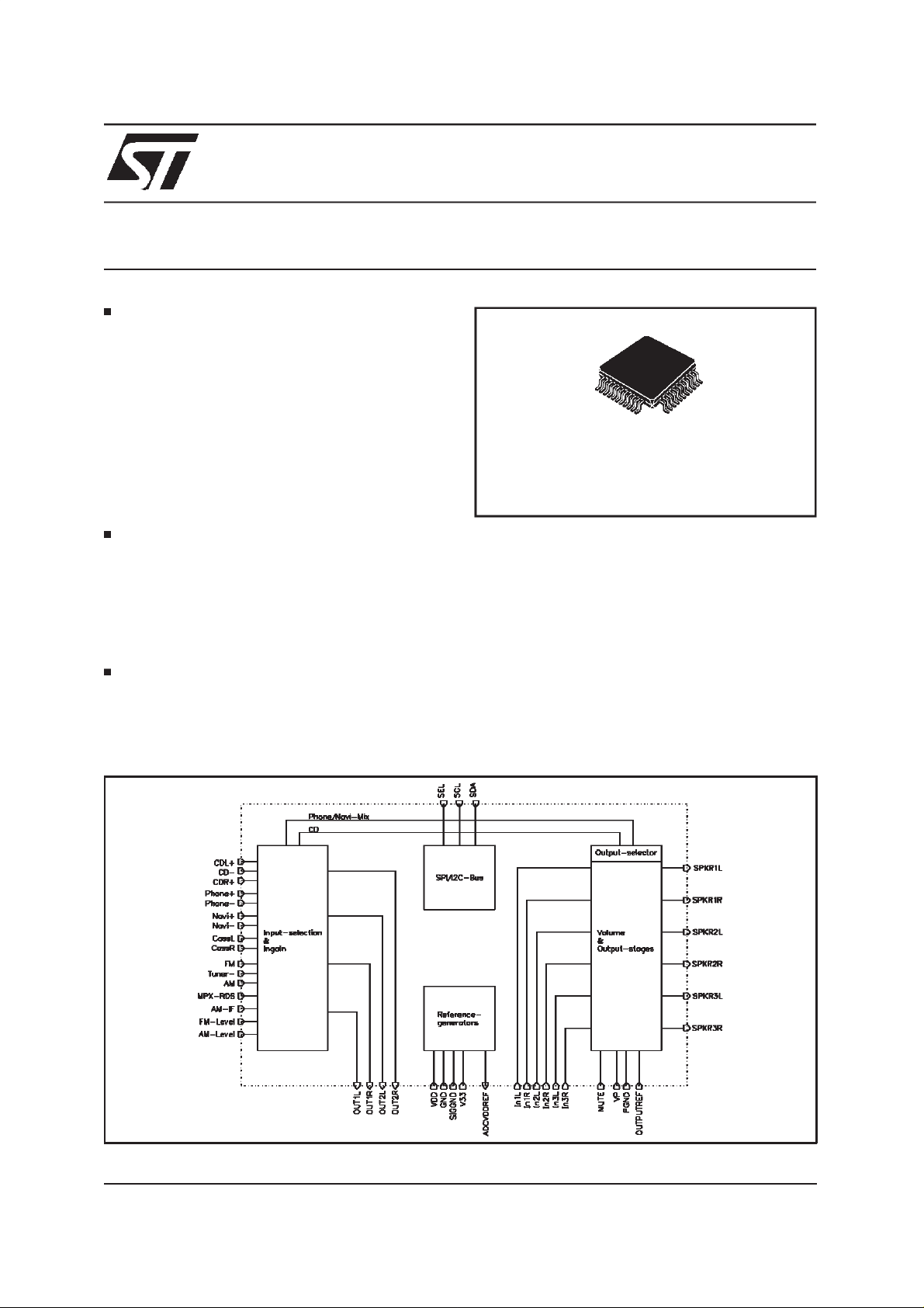
BLOCK DIAGRAM
2
C BUS INTERFACE
TDA7501
SIGNAL PROCESSOR
PRODUCT PREVIEW
TQFP44
DESCRIPTION
The Linedriver handles all analog input- and output-signals for the Digital Carradio Signal Processor TDA7501. The device contains four independent input multiplexers to select the sources
for the DSP’s four AD-converters. Four additional
gain stages allow an adaptation to run the ADCs
in best S/N condition.
The six outputs have independent volume stages
with a large dynamic range. Using a 12V-supply
the outputs are able to drive up to 4Vrms .
April 1999
This is preliminary information on a new product foreseen to be developed. Details are subject to change without notice.
1/18
TDA7501
SUPPLY
Symbol Parameter Test Condition Min. Typ. Max. Unit
V
dd
V
P
I
S8
I
S12
SVRR Ripple Rejection @ 1kHz 60 dB
ABSOLUTE MAXIMUM RATINGS
Symbol Parameter Value Unit
V
DDmax
V
Smax
T
amb
T
ESD:
All pins are protectedagainst ESD according to the MIL883 standard.
Supply Voltage 7.5 8.3 10 V
Output Supply Voltage 12 V
Supply Current V
Supply Current V
dd
P
Operating Supply Voltage V
Operating Supply Voltage V
Vdd= 8.3V 15 mA
VP= 12V 15 mA
DD
s
10.5 V
13.0 V
Operating Temperature Range -40 to 85 °C
stg
Storage Temperature Range -55 to +150 °C
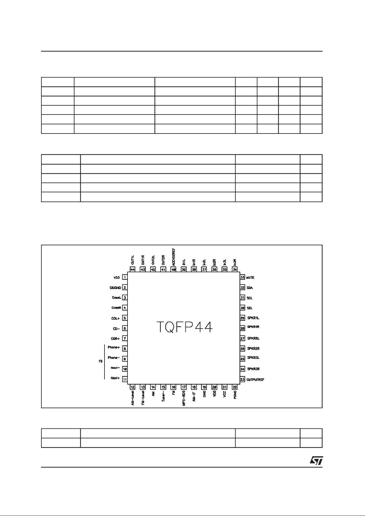
PIN CONNECTION
THERMAL DATA
Symbol Parameter Value Unit
2/18
R
th j-pins
Thermal Resistance Junction-pins Max. 65 °C/W
TDA7501
ELECTRICALCHARACTERISTICS (VDD=VS= 8.3V;T
=25°C; RL=10kΩ; all gains= 0dB;
amb
f = 1kHz; unless otherwise specified)
Symbol Parameter Test Condition Min. Typ. Max. Unit
GENERAL
V
CL
S
IN
G
IN MIN
G
IN MAX
G
STEP
V
DC
d
IN
V
DCout
R
out
QUASI DIFFERENTIAL CD STEREO INPUT (non inverting)
R
in
CMRR Common Mode Rejection Ratio V
V
N
DIFFERENTIAL PHONE/NAVIGATION/FM/AM INPUT (inverting)
R
in
CMRR Common Mode Rejection Ratio V
AM IF INPUT
R
in
CASSETTE INPUT (non inverting)
R
in
AM/FM-LEVEL INPUT
R
in
V
min
V
max
Dual MPX control (pin TUNER-)
V
CTRLMPX1
V
CTRLMPX2
V
CTRLMPX3
V
CTRLMPX4
SPEAKER OUTPUTS
R
in
G
MAX
A
MAX
Input Clipping Level 2.3 V
Input Separation 80 100 dB
Min. Input Gain 0 dB
Max. Input Gain 15 dB
Step Resolution 1 dB
DC Steps Adjacent Gain Steps 0.5 mV
G
Distortion V
MIN
OUT
to G
= 0.7V
MAX
RMS
5mV
0.002 0.08 %
Output DC-voltage pins 41..44 1.65 V
Output impedance 3 kΩ
Input Resistance (see Fig. 2) Differential 70 100 130 kΩ
=1V
CM
V
=1V
CM
@ 1kHz 45 70 dB
RMS
@ 10kHz 45 60 dB
RMS
Output-Noise 20Hz - 20kHz; unweighted 2.5 µV
Input Resistance (see Fig. 3) 35 50 65 k
=1V
CM
V
=1V
CM
@ 1kHz 40 70 dB
RMS
@ 10kHz 40 60 dB
RMS
Input Resistance 35 50 65 k
Input Resistance 70 100 130 k
Input Resistance 70 100 130 k
Minimum Input Voltage -0.4 V
Maximum Input Voltage 7 V
Control voltage for MPX 1+2 MPX1 -> MPX1 + MPX2 1.5 V
Control voltage for MPX2 MPX1 + MPX1 -> MPX2 4 V
Control voltage for MPX 1+2 MPX2 -> MPX1 + MPX2 3.5 V
Control voltage for MPX1 MPX1 + MPX2 -> MPX2 1 V
Input Impedance 35 50 65 kΩ
Max. Gain single supply mode
dual supply mode
Max. Attenuation single supply mode
dual supply mode
15
21
-79
-73
RMS
Ω
Ω
Ω
Ω
dB
dB
dB
dB
3/18
TDA7501
ELECTRICALCHARACTERISTICS (continued)
Symbol Parameter Test Condition Min. Typ. Max. Unit
A
STEP
A
MUTE
E
E
V
DC
V
DCOUT
V
CLIP
R
L
C
L
R
OUT
V
N
S/N Signal to Noise Ratio BW = 20Hz-20kHz V
d
out
S
C
ADCVDDREF (CODEC reference)
I
maxadc
BUS INPUTS
V
low
V
high
Step Resolution 1 dB
Output Mute Attenuation 80 100 dB
Attenuation Set Error from +15 to -40dB 2 dB
DC Steps Adjacent Attenuation Steps 0.1 3 mV
Output DC-voltage single supply mode
dual supply mode
4.15
outref
Output Clipping Level d = 0.3%, VCC=VDD= 8.3V
gain = 0dB
gain = 6dB
d = 0.3%, VCC= 12V
V
= 8.3V gain = 0dB
DD
2.3
2.8
4V
Output Load Resistance AC-coupled 5 k
Output Load Capacitance 10 nF
Output Impedance 30 120
Output Noise BW = 20Hz-20kHz muted 0dB
muted 6dB
gain = 0dB
gain = 6dB
=2V
O
RMS
RMS
distortion V
OUT
=1V
VO=4V
; all stages 0dB 0.005 0.08 %
RMS
3
7.5
10
13
106
110
Channel Separation left/right 80 100 dB
Max. Output Current pin 40 5 mA
Voltage for logic ”0” inputs SEL, SCL,SDA,MUTE 0.8 V
Voltage for logic ”1” inputs SEL, SCL,SDA,MUTE 2.4 V
V
V
V
V
RMS
RMS
RMS
Ω
Ω
µ
µ
µV
µ
dB
dB
V
V
V
4/18
TDA7501
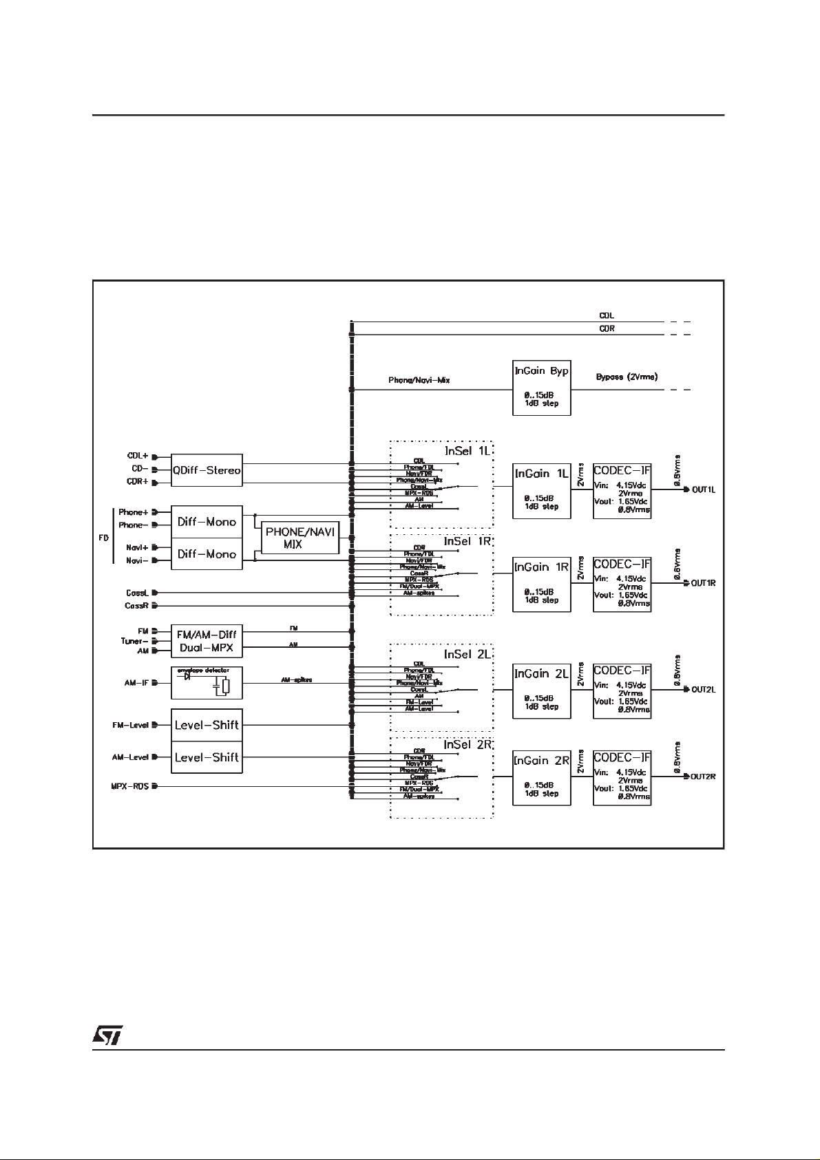
DESCRIPTIONOF THE INPUT PART
On the input side, the DSPLD (see figure 1) connects the external audio- and tuner-signals to the
four AD-converters of the Digital Carradio Signal
Processor TDA7500. The audio signals are adjusted by theinput gainstage to the internal refer-
Figure 1. Input part.
ence signal with 2V rms referred to 4.15V (=V33
à 1.2575). The following CODEC-interface attenuates the 2V
rms
to 0.8V
referred to the
rms
CODEC’s reference voltage of 1.65V which allows a DC-couplingto the TDA7500.
Input Stages
The decive offers several input stages for the different signals which have to be handled by the
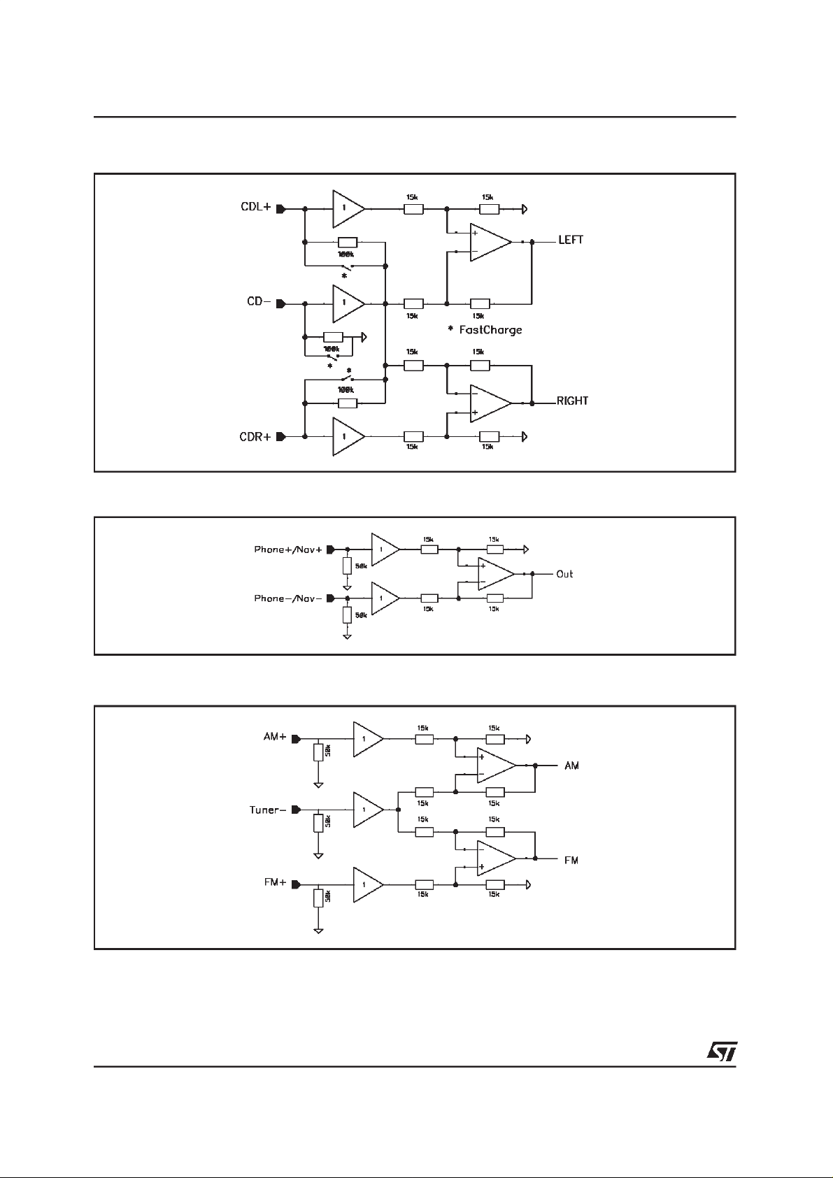
system. A quasi differential input (see figure 2)
can be used for (external) CD-changer. The two
mono differential inputs allow the connection of
Phone and Navigation(see figure 3) or it couldbe
used as fully differentialstereo input. Additionally
a single-ended stereo input is available for Cassette applications. The lower part of the input
section is dedicated to the tuner signals. Another
quasi differential input (see figure 4) is used to
connect AM and FM referred to the tuner reference (Tuner-). This concept supports also double
tuner systems. Also two seperate level inputs are
present which are followed by level-shiftersto allow the use of the TDA7500’s ADCs. For AM
noise blanking an envelope-detector driven by
the AM-IF is also available.
5/18
TDA7501
Figure 2. Quasi differential input-stage.
Figure 3. Mono differential input-stage.
Figure 4. Differentialinput-stagefor AM/FM.
6/18

TDA7501
Dual MPX mode
The TDA7501is able to support a twin tuner concept via the Dual-MPX-Mode. In this configuration
the MPX-pin and the AM-pin are acting as MPX1
and MPX2 inputs. The DC-Voltage at the
TUNER- -pin controls whether one or
Figure 4. Block diagram Dual MPX.
both MPX-signals are used to decode the stereo
FM-signal (see figure 4 Please note that the
thresholds have a hysteresis of 500mV. During
this mode the highohmic-mute acts on both inputs in parallel.
For the programming of the Dual-MPX-Mode see
the programmingsection.
7/18

TDA7501
DESCRIPTIONOF THE OUTPUT PART
The TDA7501 has 6 independent outputstage
with volume control. The first 4 (main) outputs
have an input selector which allows to select besides the DAC-outputs CD-direct or Phone/Navigation-mix. In addition one can mix the SPKR1
with Phone/Navigationso that traffic or navigation
announcementscan bypass the DSP (see figure
5).
The TDA7500 CODEC outputs have a maximum
Figure 5. Output part.
output voltage of 0.5Vrms . To obtain 4Vrms , (in
the dual supply mode only) the signal is first amplified to have a reference amplitude of 2V rms.
The following volume stage offers up to 15dB
gain which gives along with the programmable
6dB gain in the output-stage enough overdrive
capability. To achieve the maximum output swing
of 4Vrmsthe device must be supplied with an additional supply of 12V. With a single supply (V
dd
=VCC= 8.3V) 2.8Vrms are obtained at the output
at maximum.
8/18

Figure 6. Level-diagram.
TDA7501
TDA7501
REFERENCECONCEPT
For the input section the TDA7501 generates the
internal reference voltage by multiplying the V33
voltage by 1.2575.
The V33 voltage is also buffered and fed back to
the CODEC where it is used to generate all necessary references. For best performance it is recommended to filter the V33 reference pin by
means of a passive second order lowpass as
shown in figure 7 This concept allows a direct DC
coupling betweenthe TDA7501 and the DSP
because of the accurate matching of DC levels.
On the output side the TDA7501 offers two main
Figure 7. Referencevoltage generation
TDA7500
modes: a single supply and a dual supply mode.
Dual supply mode
In this mode the outputs are able to provide up to
4V rms with a minimum supply V
of 12V as
CC
well as a output reference voltage set to half of
(bit D0 of the mode select byte set to ’1’). If
V
CC
the switch D1/byte mode select is open the output reference voltage must be defined externally
e.g. a zener diode with RC-lowpass. If the switch
is closed the reference voltage will be half of V cc
and only an external capacitorhasto be added.
TDA7501
9/18

TDA7501
Single supply mode
If V
the maximum possible output swing is about 2.8V
rms . The output reference voltage pin can be left
open or otherwise the internal voltage divider can
be used to generate for the outputs a V
ence.
DIGITAL BUS
The TDA7501 digital interface offers two different
protocols: SPI and I
SEL-pin has to beconnectedto V
at the SEL-pin is more than about 1V below the
Figure 8. Timing diagram for the SPI bus mode.
and Vddare connected to a single supply
CC
CC
2
C. To select I2C-mode the
. If the voltage
DD
/2 refer-
voltage the interface switches to SPI-mode.
V
DD
In both cases the interface is able to work with a
3.3V microprocessor as well as with a 5V microprocessor. For details of both protocols refer to
the programmingsection.
SPI BUS MODE
Interface protocol
The TDA7501SPI interfaceprotocol comprises:
- a subaddressand
- a sequenceof n databytes
each consistingof 8 bits (see figure 8).
2
C BUS MODE
I
Interface Protocol
The interfaceprotocol comprises:
-a start condition (S)
-a chip address byte (writemode only)
-a subaddress byte
-a sequenceof data (N-bytes + acknowledge)
-a stop condition (P)
CHIP ADDRESS
MSB LSB MSB LSB MSB LSB
S10001100
ACK 00I0SA3 SA2SA1SA0 ACK DATA ACK P
SUBADDRESS DATA 1...DATA n
ACK = Acknowledge
S = Start
P = Stop
10/18

TDA7501
SOFTWARESPECIFICATION FOR BOTH MODES
Auto increment
If bit I in the subaddressbyte is set to ”1”, the autoincrementof the subaddressis enabled.
Reset condition
A Power-On-Reset is invoked if the Supply-Voltage V dd is below than 3.5V. After POR the following
data is written automaticallyinto the registers of all subaddresses:
MSB LSB
11111110
Subaddresses
MSB LSB
D7 D6 I D4 SA3 SA2 SA1 SA0
0
0
0
0
0
0
0
0
1
1
1
1
1
1
0
1
0 0 0 must be ”0”
0
0
0
0
1
1
1
1
0
0
0
0
1
1
The programming after POR is marked bold-face
in the programmingtables.
With this programming all the outputs are muted
to their correspondingreferencevoltages.
Input selector 1L
0
0
1
1
0
0
1
1
0
0
1
1
0
0
0
Input selector 1R
1
Input selector 2L
0
Input selector 2R
1
Bypass selector
0
Configuration
1
Mode select
0
Output selector
1
Volume 1L
0
Volume 1R
1
Volume 2L
0
Volume 2R
1
Volume 3L
0
Volume 3R
1
Autoincrement mode off
Autoincrement mode on
Input selector1L..3R, bits D7..D3(subaddresses0..3)
Name
MSB LSB
D
0
0
0
0
0
0
0
0
1
1
1
1
1
1
1
1
D
7
0
0
0
0
1
1
1
1
0
0
0
0
1
1
1
1
D
6
0
0
1
1
0
0
0
1
0
0
1
1
0
0
0
1
D
5
0
1
0
1
0
1
0
1
0
1
0
1
0
1
0
1
D
4
0
1
D
3
D
2
D
1
Function
0
mute
off
on
gain
15dB
14dB
13dB
12dB
11dB
10dB
9dB
8dB
7dB
6dB
5dB
4dB
3dB
2dB
1dB
0dB
11/18

TDA7501
Input selector1L, bits D2..D0(subaddresses0)
MSB LSB
D
D
7
D
6
D
5
D
4
D
3
0
0
0
0
1
1
1
1
D
2
1
0
0
1
1
0
0
1
1
Input selector1R, bits D2..D0(subaddresses1)
MSB LSB
D
D
7
D
6
D
5
D
4
D
3
0
0
0
0
1
1
1
1
D
2
1
0
0
1
1
0
0
1
1
D
0
source select
Function
CDL
0
Phone/FDL
1
Navigation/FDR
0
Phone/Navigation mix
1
CassL
0
MPX-RDS
1
AM
0
AM-level
1
Function
D
0
source select
CDR
0
Phone/FDL
1
Navigation/FDR
0
Phone/Navigation mix
1
CassR
0
MPX-RDS
1
FM (or MPX1/MPX2 in Dual MPX mode)
0
AM-spikes
1
Input selector2L, bits D2..D0(subaddresses2)
MSB LSB
D
D
7
D
6
D
5
D
4
D
3
0
0
0
0
1
1
1
1
D
2
1
0
0
1
1
0
0
1
1
Input selector2R, bits D2..D0(subaddresses3)
MSB LSB
D
D
7
D
6
D
5
D
4
D
3
0
0
0
0
1
1
1
1
D
2
1
0
0
1
1
0
0
1
1
D
0
source select
Function
CDL
0
Phone/FDL
1
Navigation/FDR
0
Phone/Navigation mix
1
CassL
0
AM
1
FM-level
0
AM-level
1
Function
D
0
source select
CDR
0
Phone/FDL
1
Navigation/FDR
0
Phone/Navigation mix
1
CassR
0
MPX-RDS
1
FM (or MPX1/MPX2 in Dual MPX mode)
0
AM-spikes
1
12/18

Bypass selector(subaddress 4)
TDA7501
MSB LSB
D
D
7
D
6
D
5
D
4
D
3
0
0
0
0
1
1
1
1
D
2
0
0
1
1
0
0
1
1
D
1
0
1
0
1
0
1
0
1
1 must be ”1”
0
0
0
0
0
0
0
0
1
1
1
1
1
1
1
1
0
0
0
0
1
1
1
1
0
0
0
0
1
1
1
1
0
0
1
1
0
0
0
1
0
0
1
1
0
0
0
1
0
1
0
1
0
1
0
1
0
1
0
1
0
1
0
1
Function
0
mix level phone/navigation
0/mute
-1.6dB/-15.5dB
-3.6/-9.6dB
-6/-6dB
-9.6/-3.6dB
-15.5/-1.6dB
mute/0dB
mute
gain
15dB
14dB
13dB
12dB
11dB
10dB
9dB
8dB
7dB
6dB
5dB
4dB
3dB
2dB
1dB
0dB
Mode select (subaddress5)
MSB LSB
D
D
7
0
1
D
6
D
5
D
4
D
3
D
2
1
0
1
0
1
0
1
1 must be ”1”
0
1
0
1
D
0
Function
output gain
odB
0
+6dB
1
reference voltage setting for output
internal reference (V33*1.25)
external reference
internaldivider for outputreference voltage
connected to VCC/2
disconnected
fastcharge (switches at CD input)
open
closed
RDS-mute (high impedance)
muted
unmuted
mute pin function I
”0” does not activate the output mute
”1” activates the output mute
mute pin function II
”0” activates the high impedance mute
”1” does notactivate the high impedance mute
13/18

TDA7501
Configuration(subaddress 6)
MSB LSB
D
D
7
D
6
D
5
D
4
D
3
D
2
1
0
0
1
1
0
0
1
1
0
1
0
1
1 must be ”1”
0
1
0
0
1
1
0
1
0
1
Output selector(subaddress7)
MSB LSB
D
D
7
0
0
1
1
D
6
D
5
D
4
D
3
D
2
1
0
0
1
1
0
0
1
1
0
0
1
1
0
1
0
1
0
1
0
1
0
1
0
1
D
0
AM-IF rectifier gain
Function
+18dB
0
+15.5dB
1
+12dB
0
+6dB
1
AM-IF rectifier corner frequency
14kHz
18.5kHz
28kHz
56kHz
Dual MPX mode
on (control through Tuner-voltage)
off
forced Dual MPX control
MPX1 (allows automatic selection)
MPX2 (overwrites automatic selection)
MPX1+MPX2 (overwrites automatic selection)
MPX1 (overwrites automatic selection)
Function
D
0
source select SPKR 1L
Bypass
0
CDL
1
Phone/Navigation mix / IN1L
0
IN1L
1
source select SPKR 1R
Bypass
CDL
Phone/Navigation mix / IN1R
IN1R
source select SPKR 2L
Bypass
CDL
mute
IN2L
source select SPKR 2R
Bypass
CDL
mute
IN2R
14/18

Volume speaker outputs(subaddresses 8...13)
TDA7501
MSB LSB
D
D
7
1
:
1
1
0
0
:
0
0
:
0
0
x
D
6
0
:
0
0
0
0
:
0
0
:
1
1
1
D
5
0
:
0
0
0
0
:
0
0
:
0
0
1
D
4
0
:
0
0
0
0
:
0
1
:
0
0
x
D
3
1
;
0
0
0
0
:
1
0
:
1
1
x
D
2
1
;
0
0
0
0
:
1
0
:
1
1
x
D
1
1
;
0
0
0
0
:
1
0
:
1
1
x
0
1
;
1
0
0
1
:
1
0
:
0
1
x
+15dB
:
+1dB
0dB
0dB
-1dB
:
-15dB
-16dB
:
-78dB
-79dB
Mute
Function
The unused subaddresses 14/15 must be programmed to ”11111110”to allow software compatibility to future extensions.
15/18

TDA7501
Figure 9. Applicationdiagram.
TDA7500
TDA7501
16/18

TDA7501
DIM.
mm inch
MIN. TYP. MAX. MIN. TYP. MAX.
A 1.60 0.063
A1 0.05 0.15 0.002
0.006
A2 1.35 1.40 1.45 0.053 0.055 0.057
B 0.30 0.37 0.45 0.012 0.014 0.018
C 0.09 0.20 0.004
0.008
D 12.00 0.472
D1 10.00 0.394
D3 8.00 0.315
e 0.80 0.031
E 12.00 0.472
E1 10.00 0.394
E3 8.00 0.315
L 0.45 0.60 0.75 0.018 0.024 0.030
L1 1.00 0.039
K 0°(min.),3.5°(typ.),7°(max.)
OUTLINE AND
MECHANICAL DATA
TQFP44 (10 x 10)
D
D1
A1
2333
34
B
44
1
e
11
TQFP4410
22
E
E1
12
L
0.10mm
.004
Seating Plane
B
K
A
A2
C
17/18

TDA7501
Information furnished is believed to be accurate and reliable. However, STMicroelectronics assumes no responsibility for the consequences
of use of such information nor for any infringement of patents or other rights of third parties which may result from its use. No license is
granted by implication or otherwise under any patent or patent rights of STMicroelectronics. Specification mentioned in this publication are
subject to change without notice. This publication supersedes and replaces all information previously supplied. STMicroelectronics products
are not authorized for use as critical components in life support devices or systems without express written approval of STMicroelectronics.
The STlogo is a registeredtrademark of STMicroelectronics
1999 STMicroelectronics – Printed in Italy – All Rights Reserved
STMicroelectronics GROUP OF COMPANIES
Australia - Brazil - Canada - China - France - Germany - Italy - Japan - Korea - Malaysia - Malta - Mexico - Morocco - The Netherlands -
Singapore- Spain - Sweden - Switzerland- Taiwan - Thailand - United Kingdom- U.S.A.
http://www.st.com
18/18
 Loading...