


®
y
q
DIGITAL AM/FM SIGNAL PROCESSOR
FULL SOFTWARE FLEXIBILITY WITH TWO
24X24 BIT DSP CORES
AM/FM PROCESSING
AUDIO-PROCESSING AND SOUND-PROC-
ESSING
HARDWARE RDS FILTER, DEMODULATOR
& DECODER
INTEGRATED CODEC
IIC AND SPI CONTROL INTERFACES
SPI DEDICATED TO DISPLAY MICRO
6 CHANNEL SERIAL AUDIO INTERFACE SAI
SPDIF RECEIVER WITH SAMPLE RATE
CONVERTER
EXTERNAL MEMORY INTERFACE
DOUBLE DEBUG INTERFACE
ON-CHIP PLL
5V-TOLERANT 3V I/O INTERFACE
MULTIFUNCTION GENERAL PURPOSE I/O PORTS
TDA7500
PRODUCT PREVIEW
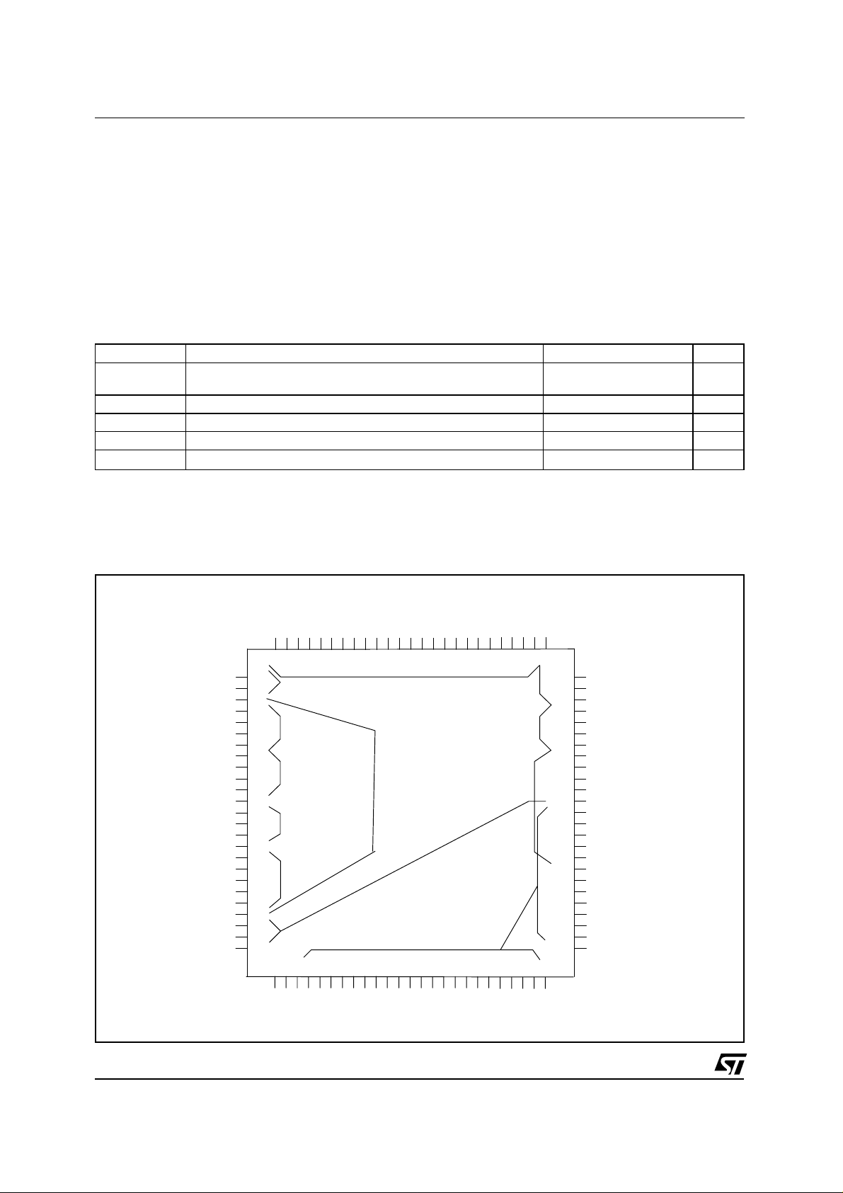
TQFP100 Power with Slug Down
DESCRIPTION
The TDA7500 is an integrated circuit implementing a fully digital, integrated and advanced solution to perform the signal processing in front of
the power amplifier and behind the AM/FM tuner
or any other audio sources. The chip integrates
two 43 MIPs DSP cores: one for stereo decoding,
noise blanking, weak signal processing and multi-
BLOCK DIAGRAM
analog audio in
AM-IF
CC
CD
tel,navi
AM/FM lev.
AM/FM mpx
RDS mpx
uP control
Main micro
Display uP
Spectrum Analyser
CLK in
8.55MHz
Data, ctl
128k (4M) x 8
(1 I/O)
Address
Audio Bus 6 ch.
dig. aud. out
clkt, wst, clkr, wsr
dig. aud. in
CD input
CDC input
MD input
RDS bit/blk Int.
RDS
Error corrected RDS blocks
alternativel
RDS clk, dat,
1
2
3
4
2
3
1
(4 I/O's)
(4 I/O's)
Audio Bus Synch.
8+3
(2 I/O's)
(2 I/O's)
(1 I/O)
(4 I/O's)
:
ual, ARI
4
4
17
3
4
2
4
4
RDS
Mute
Input Multiplexer,
Analog Level Adjus t
Σ∆
Modulator
Σ∆
Modulator
Σ∆
Modulat or
Σ∆
Modulat or
IIC / SPI
SPI
XTAL Osc.,
PLL
Ext. Memory
Interface
Serial A u d io
Interface
SPDIF
Interface
Mux
Grp & blk
sync., error
SPI
correction
supply
Cref
2
2
AM
Noise
Detector
VDD GND
32
Decimation
Filter
Decimation
Filter
1 stereo channel
Sample Rate
Converter
Demod.
2 channel analog bypass
Exchange
Interface
RDS
Filter
3
IIC
CODEC-ref
Voltage
Ref.
Codec
Ctl Reg.
Test I/F
DSP Orpheus Core
including 12 GPIO•s including 12 GPIO•s
FM processing,
AM proc es sing ,
Traffic mem., Dolby,
Speech synth., etc...
Debug, Test Interface
Oversampling
Filter
Oversampling
Filter
Oversampling
Filter
X Register
Ram 512
Y Register
Ram 512
Program
Ram 1024
Rom 256
DSP1
VS SigGnd
Output
Analog Volume Co nt rol,
select.
Line Drive r
Noise
Shaper
Noise
Shaper
Noise
Shaper
X bus 0X bus 1
DSP Orpheus Core
Audi o processing ,
Sound pro c es s ing
Debug, Test Interface
DSP0
X Register
Ram 512
Y Register
Ram 512
Program
Ram 5632
Rom 256
RefOut
DAC-ref
SC Filter
SC Filter
SC Filter
SC Filter
SC Filter
SC Filter
6
6
5
5
2
4
4
signal/line out
Int
Reset
VDD
GND
Test
(3 I/O's)
(3 I/O's)
September 1999
1/14
This is preliminary information on a new product foreseen to be developed. Details are subject to change without notice.
y
g
TDA7500
path detection and one for sound processing. An
I2C/SPI interface is implemented for control and
communication with the main micro.
A separate SPI is available to interface the display micro.
The DSP cores are integrated with their associated data and program memories. The peripherals and interfaces I
2
C, SPI, Serial Audio Interface
(SAI), PLL Oscillator, External Memory Interface,
(EMI), General Purpose I/O register (Port A) and
by DSP0, whereas the A/D registers, the SPDIF
and the General Purpose I/O register (Port B) are
connected to and controlled by DSP1. The Debug
and Test Interface are connected to both DSP
cores.
The TDA7500 is supposed to be used in kit with
the TDA7501 or any other device of the same
family. Thanks to the serial audio interface also
digital sources can be processed and a direct
output to a digital bus is also available.
the D/A registers are connected to and controlled
ABSOLUTE MAXIMUM RATINGS
Symbol Parameter Value Unit
VDD
VCC
Power supplies Digital
Analog
4.6
4.6
Analog Input Voltage -0.5 to (VDD+0.5) V
Digital Input Voltage -0.5 to (VCC+0.5) V
T
amb
T
stg
Warning: Operation at or beyond these limit may result in permanent damage to the device.
Normal operation is not guaranteed at these extremes.
Operating Temperature Range -40 to 85 °C
Storage Temperature -55 to 150 °C
PIN CONNECTION
CODEC0
CODEC2
COUT<5>
COUT<4>
COUT<3>
COUT<2>
COUT<1>
CODEC1
CVDD0
CGND0
COUT<0>
S2DREF
COIN<3>
COIN<2>
COIN<1>
VREF0
VREF1
VREF2
COVDD1
COIN<0>
COGND1
COVDD2
DBRQN0
GND2
VDD2
V
V
2/14
DSP0 GPIO0
DSP0 GPIO1
DSP0 GPIO2
DSP0 GPIO3
DSP0 GPIO4
DSP0 GPIO5
DSP0 GPIO6
DSP0 GPIO7
DSP1 GPIO4
DSP1 GPIO3
DSP1 GPIO2
DSP1 GPIO1
DSP1 GPIO0
TESTEN
TESTSE
NRESET
SCKM
MISOM
MOSIM
SSM
SCKD
MISOD
MOSID
SSD
AVDD
XTI
XTO
CLKIN
AGND
RDSINT
RDSARI_SCLK
RDSQAL_SO
RDSDAT_SI
RDSCLK_SS
INT
SRCCD
SRCMD
GND1
999897
100
1
2
3
4
5
6
7
8
9
10
11
12
13
14
15
16
17
18
19
20
21
22
23
24
25
26
VDD1
9695949392
Test
IIC/SPI master
SPI displa
PLL oscillator
RDS
SPDIF + Sample Rate Converter
272829
3031323334
CGND1
DSRA<7>
DSRA<6>
DSRA<5>
CVDD1
898887
373839
SRA<0>
SRA<1>
8685848382
4041424344
SRA<2>
SRA<3>
SRA<4>
90
91
CODEC
Control Inputs
35
36
DSRA<4>
DSRA<3>
DSRA<2>
DSRA<1>
DSRA<0>
SRA<5>
SRA<6>
SRA<7>
8180797877
Debug DSP0
DSP1
Debu
SAI
EMI
4546474849
SRA<8>
SRA<9>
SRA<10>
SRA<11>
SRA<12>
76
75
74
73
72
71
70
69
68
67
66
65
64
63
62
61
60
59
58
57
56
55
54
53
52
51
50
CGND2
DBCK0OS01
DBIN0OS00
DBOUT0
DBRQN1
DBCK1_OS11
DBIN1_OS10
DBOUT1
LRCKR
SCKR
LRCKT
SCKT
SDI0
SDI1 / SRA<21>
SDI2 / SRA<20>
SDO0 / SRA<19>
SDO1 / SRA<18>
SDO2 / SRA<17>
CASALE
DRD
DWR
SRA<16>
SRA<15>
SRA<14>
SRA<13>
CVDD2
DSP0 GPIO9
DSP0 GPIO11
DSP0 GPIO10
DSP1 GPIO9
DSP1 GPIO11
DSP1 GPIO10
SRCCDC
DSP1 GPIO5
DSP1 GPIO6
DSP1 GPIO7
DSP1 GPIO8
DSP0 GPIO8
TDA7500
PIN DESCRIPTION
N° NAME TYPE DESCRIPTION
1 GND1 Ground pin dedicated to the digital periphery.
2 VDD1 Supply pin dedicated to the digital periphery.
3 TESTEN I Test Enable (Input). When active, puts the chip into test mode and
4 TESTSE I SCAN Enable (Input). When active with TESTEN also active,
5 NRESET I System Reset (Input). A low level applied to NRESET input
6 SCKM/DSP0_GPIO0 I/O I
7 MISOM/DSP0_GPIO1 I/O I
8 MOSIM/DSP0_GPIO2 I/O SPI Master Output Slave Input Serial Data (Input/Output)/General
9 SSM/DSP0_GPIO3 I SPI Slave Select (Input)/General Purpose I/O (Input/Output). If SPI
10 SCKD/DSP0_GPIO4 I SPI Bit Clock (Input)/General Purpose I/O (Input/Output). SPI bit
11 MISOD/DSP0_GPIO5 I/O SPI Master Input Slave Output Serial Data (Input/Output)/General
12 MISOD/DSP0_GPIO6 I/O SPI Master Output Slave Input Serial Data (Input/Output)/General
13 SSD/DSP0_GPIO7 I SPI Slave Select (Input)/General Purpose I/O (Input/Output).
14 CLKIN I Clock Input pin (Input). Clock from external digital audio source to
15 AVDD audio source to synchronize the internal PLL.
16 XTI I Crystal Oscillator Input (Input). External Clock Input or crystal
17 XTO O Crystal Oscillator Output (Output). Crystal Oscillator output drive.
18 AGND Ground pin dedicated to the PLL
19 RDSINT/DSP1_GPIO4 O RDS bit/block interrupt (Output)/General Purpose I/O
muxes the XTI clock to all flip-flops. When TEST_SE is also
active, the scan chain shifting is enabled.
controls the shifting of the internal scan chains. When active with
TESTEN not active, sets all tri-state outputs into hi-impedance
mode
initializes the IC.
2
C Serial Clock Line (Input/Output)/SPI Bit Clock (Input)/General
Purpose I/O (Input/Output). Clock line for I
2
C bus. Schmitt trigger
input. If SPI interface is enabled, behaves as SPI bit clock.
Optionally it can be used as general purpose I/O controlled by
DSP0.
2
C Serial Data Line (Input/Output)/SPI Master Input Slave Output
Serial Data (Input/Output)/General Purpose I/O (Input/Output).
Data line for I
2
C bus. Schmitt trigger input. If SPI is enabled,
behaves as Serial Data Input when in SPI Master Mode and Serial
Data Output when in SPI Slave Mode. Optionally it can be used as
general purpose I/O controlled by DSP0.
Purpose I/O (Input/Output). Serial Data Output when in SPI
Master Mode and Serial Data Input when in SPI Slave Mode.
Optionally it can be used as general purpose I/O controlled by
DSP0.
is enabled, behaves as Slave Select line for SPI bus. Optionally it
can be used as general purpose I/O controlled by DSP0.
clock. Schmitt trigger input. Optionally it can be used as general
purpose I/O controlled by DSP0.
Purpose I/O (Input/Output). Schmitt trigger input. Behaves as
Serial Data Input when in SPI Master Mode and Serial Data
Output when in SPI Slave Mode. Optionally it can be used as
general purpose I/O controlled by DSP0.
Purpose I/O (Input/Output). Serial Data Output when in SPI
Master Mode and Serial Data Input when in SPI Slave Mode.
Optionally it can be used as general purpose I/O controlled by
DSP0.
Behaves as Slave Select line for SPI bus. Optionally it can be
used as general purpose I/O controlled by DSP0.
synchronize the internal PLL.
Oscillator input.
(Input/Output). Provides an interrupt to the main micro. Optionally
it can be used as general purpose I/O controlled by DSP1.
3/14
TDA7500
PIN DESCRIPTION
N° NAME TYPE DESCRIPTION
20 RDSARI_SCK/DSP1_GPIO3 O SPI Bit Clock (Input)/ARI indicator (Output)/General Purpose I/O
21 RDSQAL_SO/DSP1_GPIO2 O SPI Slave Output Serial Data (Output)/RDS Bit Quality
22 RDSDAT_SI/DSP1_GPIO1 I SPI Slave Input Serial Data (Input)/RDS Bit Data (Output)/General
23 RDSCLK_SS/DSP1_GPIO0 I SPI Chip Select (Input)/RDS Bit Clock (Output)/General Purpose
24 INT I External interrupt line (Input). When this line is asserted low, the
25 CGND1 Ground pin dedicated to the digital core part.
26 CVDD1 Supply pin dedicated to the digital core part.
27 SCRCCD I SPDIF Input 1 (Input). Stereo SPDIF input to connect a digital
28 SCRCMD I SPDIF Input 2 (Input). Stereo SPDIF input to connect a digital
29 DSRA<7> I/O DSP SRAM Data Lines<7> (Input/Output). When in SRAM Mode
30 DSRA<6> I/O DSP SRAM Data Lines<6> (Input/Output). When in SRAM Mode
31 DSRA<5> I/O DSP SRAM Data Lines<5> (Input/Output). When in SRAM Mode
32 DSRA<4> I/O DSP SRAM Data Lines<4> (Input/Output). When in SRAM Mode
33 DSRA<3> I/O DSP SRAM Data Line<3> (Input/Output)/DSP DRAM Data
34 DSRA<2> I/O DSP SRAM Data Line<2> (Input/Output)/DSP DRAM Data
35 DSRA<1> I/O DSP SRAM Data Line<1> (Input/Output)/DSP DRAM Data
36 DSRA<0> I/O DSP SRAM Data Line<0> (Input/Output)/DSP DRAM Data
37 SRA<0> O DSP SRAM Address Line<0> (Output)/DSP DRAM Address
38 SRA<1> O DSP SRAM Address Line<1> (Output)/DSP DRAM Address
(continued)
(Input/Output). Schmitt trigger input. If SPI interface is enabled,
behaves as SPI bit clock. Optionally it provides the ARI indication
bit. Optionally it can be used as general purpose I/O controlled by
DSP1.
(Output)/General Purpose I/O (Input/Output). If SPI is enabled,
behaves as Serial Data Output. Optionally it provides the RDS
serial data quality information. Optionally it can be used as general
purpose I/O controlled by DSP1.
Purpose I/O (Input/Output). If SPI is enabled, behaves as Serial
Data Input. Optionally it provides the RDS serial data stream.
Optionally it can be used as general purpose I/O controlled by
DSP1.
I/O (Input/Output). If SPI is enabled, behaves as Chip Select line
for SPI bus. Optionally it provides the 1187.5Hz RDS Bit Clock.
Optionally it can be used as general purpose I/O controlled by
DSP1.
DSP may be interrupted.
audio source like a CD.
audio source like a MD.
this pin act as the EMI data line 7.
this pin act as the EMI data line 6.
this pin act as the EMI data line 5.
this pin act as the EMI data line 4.
Line<3> (Input/Output). This pin act as the EMI data line 3 in both
SRAM Mode and DRAM Mode.
Line<2> (Input/Output). This pin act as the EMI data line 2 in both
SRAM Mode and DRAM Mode.
Line<1> (Input/Output). This pin act as the EMI data line 1 in both
SRAM Mode and DRAM Mode.
Line<0> (Input/Output). This pin act as the EMI data line 0 in both
SRAM Mode and DRAM Mode.
Line<0> (Output). This pin act as the EMI address line 0 in both
SRAM Mode and DRAM Mode.
Line<1> (Output). This pin act as the EMI address line 1 in both
SRAM Mode and DRAM Mode.
4/14
TDA7500
PIN DESCRIPTION
N° NAME TYPE DESCRIPTION
39 SRA<2> O DSP SRAM Address Line<2> (Output)/DSP DRAM Address
40 SRA<3> O DSP SRAM Address Line<3> (Output)/DSP DRAM Address
41 SRA<4> O DSP SRAM Address Line<4> (Output)/DSP DRAM Address
42 SRA<5> O DSP SRAM Address Line<5> (Output)/DSP DRAM Address
43 SRA<6> O DSP SRAM Address Line<6> (Output)/DSP DRAM Address
44 SRA<7> O DSP SRAM Address Line<7> (Output)/DSP DRAM Address
45 SRA<8> O DSP SRAM Address Line<8> (Output)/DSP DRAM Address
46 SRA<9> O DSP SRAM Address Line<9> (Output)/DSP DRAM Address
47 SRA<10> O DSP SRAM Address Line<10> (Output)/DSP DRAM Address
48 SRA<11> O DSP SRAM Address Line<11> (Output)/DSP DRAM Address
49 SRA<12> O DSP SRAM Address Line<12> (Output)/DSP DRAM Address
50 CGND2 Ground pin dedicated to the digital core part.
51 CVDD2 Supply pin dedicated to the digital core part.
52 SRA<13> O DSP SRAM Address Line<13> (Output)/DSP DRAM Address
53 SRA<14> O DSP SRAM Address Line<14> (Output)/DSP DRAM Address
54 SRA<15> O DSP SRAM Address Line<15> (Output)/DSP DRAM Address
55 SRA<16>/DSP0_GPIO8 O DSP SRAM Address Line<16> (Output)/DSP DRAM Address
56 DWR O DSP SRAM Write Enable (Output)/DRAM Write Enable (Output).
57 DRD O DSP SRAM Read Enable(Output)/DRAM Read Enable (Output).
(continued)
Line<2> (Output). This pin act as the EMI address line 2 in both
SRAM Mode and DRAM Mode.
Line<3> (Output). This pin act as the EMI address line 3 in both
SRAM Mode and DRAM Mode.
Line<4> (Output). This pin act as the EMI address line 4 in both
SRAM Mode and DRAM Mode.
Line<5> (Output). This pin act as the EMI address line 5 in both
SRAM Mode and DRAM Mode.
Line<6> (Output). This pin act as the EMI address line 6 in both
SRAM Mode and DRAM Mode.
Line<7> (Output). This pin act as the EMI address line 7 in both
SRAM Mode and DRAM Mode.
Line<8> (Output). This pin act as the EMI address line 8 in both
SRAM Mode and DRAM Mode.
Line<9> (Output). This pin act as the EMI address line 9 in both
SRAM Mode and DRAM Mode.
Line<10> (Output). This pin act as the EMI address line 10 in both
SRAM Mode and DRAM Mode.
Line<11> (Output). This pin act as the EMI address line 11 in both
SRAM Mode and DRAM Mode.
Line<12> (Output). This pin act as the EMI address line 12 in both
SRAM Mode and DRAM Mode.
Line<13> (Output). This pin act as the EMI address line 13in both
SRAM Mode and DRAM Mode.
Line<14> (Output). This pin act as the EMI address line 14 in both
SRAM Mode and DRAM Mode.
Line<15> (Output). This pin act as the EMI address line 15 in both
SRAM Mode and DRAM Mode.
Line<16> (Output)/General Purpose I/O (Input/Output). This pin
acts as the EMI address line 16 in both SRAM Mode and DRAM
Mode. Optionally it can be used as general purpose I/O controlled
by DSP0.
This pin serves as the write enable for the EMI in both DRAM and
SRAM Mode.
This pin serves as the read enable for the EMI in both DRAM and
SRAM Mode.
5/14
 Loading...