

TDA7499
6 + 6W STEREO AMPLIFIER WITH MUTE & ST-BY
WIDE SUPPLY VOLTAGE RANGE UP TO
±18V
6 + 6W @ THD=10%,R
L
=8Ω,VS=+14V
NO POP AT TURN-ON/OFF
MUTE(POP FREE)
STAND-BY FEATURE (LOWI
q
)
SHORTCIRCUITPROTECTIONTO GND
THERMALOVERLOADPROTECTION
DESCRIPTION
The TDA7499 is class AB dual Audio power amplifier assembled in the Multiwatt package, specially designed for high quality sound application
as Hi-Fi music centers and stereo TV sets.
May 1997
Multiwatt11
ORDERING NUMBER: TDA7499
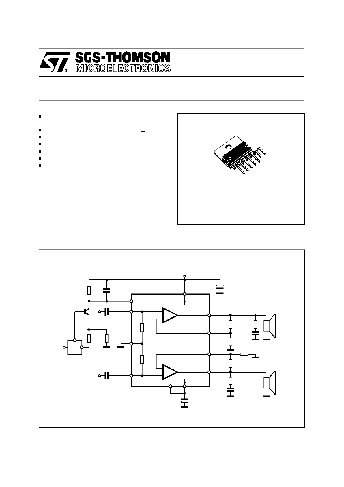
+5V
18K15K
IN (L)
1µF
15K 1µF
MUTE/
ST-BY
GND
IN (R)
1µF
4.7Ω
4.7Ω
100nF
100nF
OUT (L)
OUT (R)
1000µF
1000µF
+V
S
3
5
7
9
6
11
2
4+
+
-
-
D94AU085
RL (L)
RL (R)
-V
S
µP
560Ω
18K
IN- (L)8
10 IN- (R)
1
560Ω
18K
Figure 1: Typical ApplicationCircuit
1/7
ABSOLUTE MAXIMUM RATINGS
Symbol Parameter Value Unit
V
S
DC Supply Voltage ±20 V
I
O
Output PeakCurrent (internally limited) 2.5 A
P
tot
Power Dissipation T
case
=70°C23W
T
op
Operating Temperature 0 to 70 °C
T
stg,Tj
Storage and Junction Temperature -40to +150 °C
1
2
3
4
5
6
7
9
10
11
8
IN+(1)
IN-(1)
GND
IN-(2)
IN+(2)
-V
S
MUTE
OUTPUT(2)
+V
S
OUTPUT(1)
-V
S
TAB CONNECTED TO PIN 6
D95AU316
PIN CONNECTION(Topview)
THERMAL DATA
Symbol Description Value Unit
R
th j-case
Thermal Resistance Junction-case Max 2.8 °C/W
R
th j-amb
Thermal Resistance Junction to Ambient Max 35 °C/W
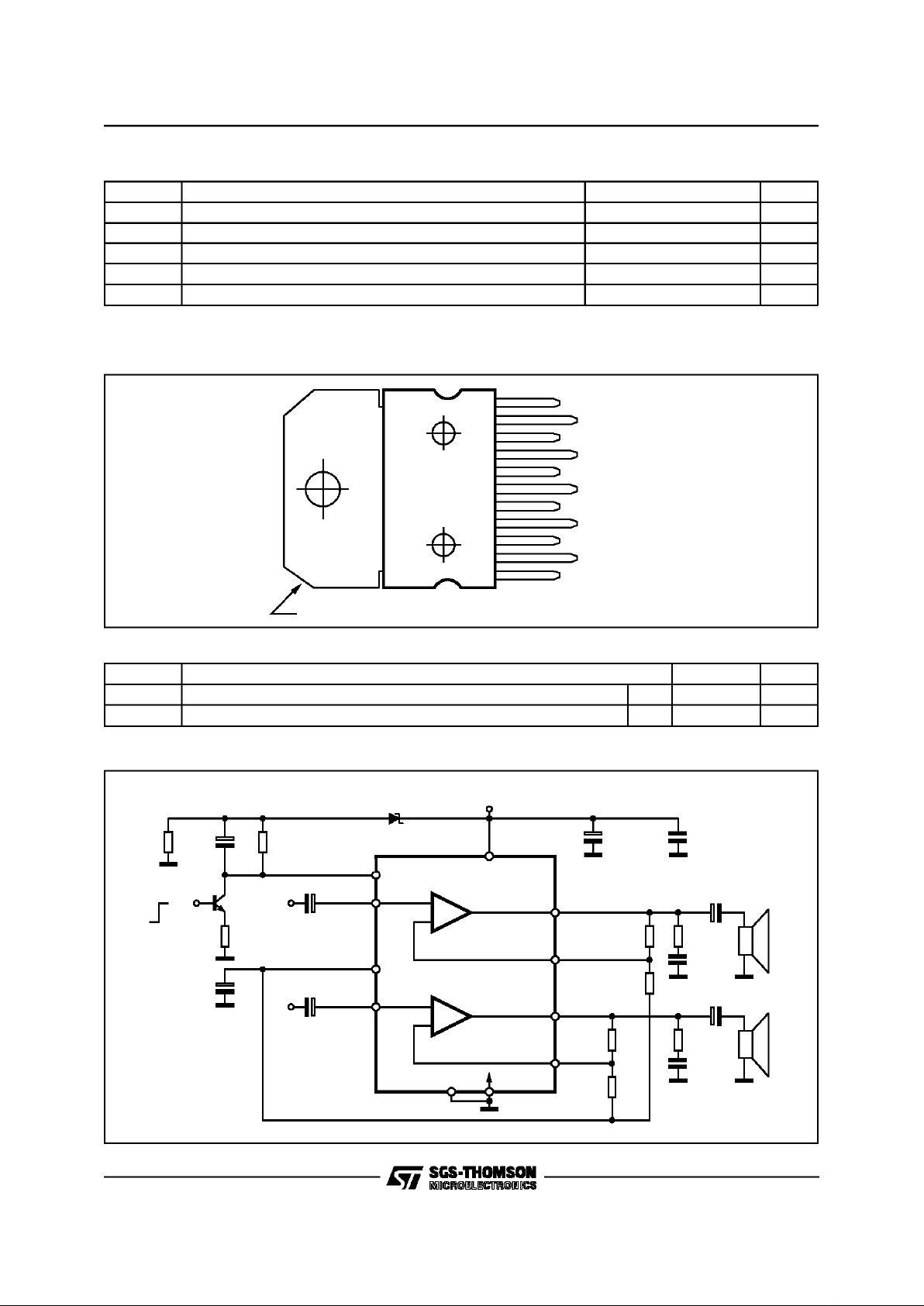
PLAY
5V
R2
15K
IN (L)
C3 1µF
R1
10K
C1
1µF
MUTE/ST-BY
IN (R)
C4 1µF
R8
4.7Ω
R7
1K
C7
0.1µF
OUT (L)
OUT (R)
C5
1000µF
+V
S
3
5
7
9
6
11
2
4+
+
-
-
D96AU444
OUT
(L)
OUT
(R)
GND
R4
30K
IN- (L)8
10
IN- (R)
1
R5
1K
R6
30K
R9
4.7Ω
C9 470µF
C10 470µF
C8
0.1µF
R3
15K
0
MUTE
Q1
BSX33
C6
0.1µF
D1 5.1V
C2
100µF
Figure 2: Single SupplyApplication
TDA7499
2/7
ELECTRICALCHARACTERISTICS (Refer to the test circuit, VS= + 14V; RS =50Ω;
G
V
= 30dB;f = 1KHz; T
amb
=25°C, unless otherwise specified.)
Symbol Parameter Test Condition Min. Typ. Max. Unit
V
S
Supply Range RL=8Ω +5 +18 V
R
L
=4Ω +5 +13.5 V
I
q
Total Quiescent Current 50 90 mA
V
OS
Input Offset Voltage –25 +25 mV
I
b
Output BiasCurrent 500 nA
P
O
Output Power THD = 10%
R
L
=8Ω ;
V
S
+ 11V; RL=4Ω
810
7.5
W
W
THD = 1%
R
L
=8Ω ;
V
S
+ 11V; RL=4
Ω
6 7.5
6
W
W
THD Total Harmonic Distortion R
L
=8Ω ;PO= 1W; f = 1KHz 0.03 %
R
L
=8Ω ;
P
O
= 0.1 to 5W; VS+ 13V;
f = 100Hz to 15KHz
0.2 0.5 %
R
L
=4Ω;PO= 1W; f = 1KHz 0.02 %
R
L
=4Ω ;VS+ 10V;
P
O
= 0.1 to 4W;
f = 100Hz to 15KHz
0.2 1 %
C
T
Cross Talk f = 1KHz
f = 10KHz 50
70
60
dB
dB
SR Slew Rate 6.5 10 V/µs
G
OL
Open Loop Voltage Gain 80 dB
e
N
Total Input Noise A Curve
f = 20Hz to 22KHz
3
48
µ
V
µV
R
i
Input Resistance 15 20 KΩ
SVR Supply Voltage Rejection
(each channel)
fr = 100Hz Vr = 0.5V 60 dB
T
j
Thermal Shut-down
Junction Temperature
145 °C
MUTE FUNCTION [ref: +V
S
]
VT
MUTE
Mute / Play Threshold -7 -6 -5 V
A
M
Mute Attenuation 60 70 dB
STAND-BY FUNCTION [ref: +V
S
] (only For Split Supply)
VT
ST-BY
Stand-by / Mute Threshold -3.5 -2.5 -.5 V
A
ST-BY
Stand-by Attenuation 110 dB
I
q ST-BY
Quiescent Current @ Stand-by 3 6 mA
TDA7499
3/7

MUTE STAND-BY FUNCTION
The pin 5 (MUTE/STAND-BY) controls the amplifier status by two different thresholds, referred to
+V
S
.
- When V
pin5
higher than = +VS - 2.5V the
amplifier is in Stand-by mode and the final
stage generatorsare off
- when V
pin5
is between +VS- 2.5V and+V
S
- 6V the final stage current generators are
switched on and the amplifier is in mute
mode
- when V
pin5
is lower than +VS - 6V the am-
plifier is play mode.
t
OFF
STDBY
MUTE MUTE
MUTE
MUTE
PLAY STDBY PLAY OFF
STDBY
20
+V
S
(V)
-20
-V
S
V
IN
(mV)
Vpin5
(V)
V
S
VS-2.5
V
S-
6
V
S
-10
I
q
(mA)
0
VOUT
(V)
D94AU086
Figure 3.
TDA7499
4/7

R3
IN (L)
C1
R2 C3
MUTE/
ST-BY
GND
IN (R)
C2
R7
R10
C8
C9
OUT (L)
OUT (R)
C6
C4
+V
S
3
5
7
9
6
11
2
4+
+
-
-
D94AU087
RL (L)
RL (R)
+V
S
-V
S
R9
R5
IN- (L)8
10 IN- (R)
1
SW1
R1
DZ
R4
SW2
C7
R8
R6
C5
Figure 4: Test and Application Circuit (StereoConfiguration).
APPLICATIONS SUGGESTION
(Demo Board Schematic)
The recommendedvalues of the external compo-
nents are those shownare the demo board schematic different values can be used: the following
table can help the designer.
COMPONENTS
RECOMMENDED
VALUE
PURPOSE
LARGER THAN
RECOMMENDED VALUE
SMALLER THAN
RECOMMENDED VALUE
R1 10KΩ Mute Circuit
Increase of Dz
Biasing Current
R2 15KΩ Mute Circuit V
pin
# 5 Shifted Downward V
pin
# 5 Shifted Upward
R3 18KΩ Mute Circuit V
pin # 5 Shifted Upward Vpin # 5 Shifted Downward
R4 15K
Ω
Mute Circuit V
pin
# 5 Shifted Upward V
pin
# 5 Shifted Downward
R5, R8 18K
Ω
Closed Loop Gain
Setting (*)
Increase of Gain
R6, R9 560Ω Decrease of Gain
R7, R10 4.7Ω Frequency Stability Danger of Oscillations Danger of Oscillations
C1, C2 1µF
Input DC
Decoupling
Higher Low Frequency
Cutoff
C3 1µF
St-By/Mute Time
Constant
Larger On/Off Time Smaller On/Off Time
C4, C6 1000µF
Supply Voltage
Bypass
Danger of Oscillations
C5, C7 0.1µF
Supply Voltage
Bypass
Danger of Oscillations
C8, C9 0.1µF FrequencyStability
Dz 5.1V Mute Circuit
(*) Closed loop gain has to be => 25dB
TDA7499
5/7

MULTIWATT11 PACKAGE MECHANICAL DATA
DIM.
mm inch
MIN. TYP. MAX. MIN. TYP. MAX.
A 5 0.197
B 2.65 0.104
C 1.6 0.063
D 1 0.039
E 0.49 0.55 0.019 0.022
F 0.88 0.95 0.035 0.037
G 1.57 1.7 1.83 0.062 0.067 0.072
G1 16.87 17 17.13 0.664 0.669 0.674
H1 19.6 0.772
H2 20.2 0.795
L 21.5 22.3 0.846 0.878
L1 21.4 22.2 0.843 0.874
L2 17.4 18.1 0.685 0.713
L3 17.25 17.5 17.75 0.679 0.689 0.699
L4 10.3 10.7 10.9 0.406 0.421 0.429
L7 2.65 2.9 0.104 0.114
M 4.1 4.3 4.5 0.161 0.169 0.177
M1 4.88 5.08 5.3 0.192 0.200 0.209
S 1.9 2.6 0.075 0.102
S1 1.9 2.6 0.075 0.102
Dia1 3.65 3.85 0.144 0.152
TDA7499
6/7

Information furnished is believed to be accurate and reliable. However, SGS-THOMSON Microelectronics assumes no responsibility for the
consequences of use of such information nor for any infringement of patents or other rights of third parties which may result from its use. No
license is granted by implication or otherwise under any patent or patent rights of SGS-THOMSON Microelectronics. Specifications mentioned in this publication are subject to change without notice. This publication supersedes and replaces all information previously supplied.
SGS-THOMSON Microelectronics products are not authorized for use as critical components in life support devices or systems without express written approval of SGS-THOMSON Microelectronics.
1997SGS-THOMSON Microelectronics - All Rights Reserved
MULTIWATT is a registered trademark of companies belonging to the SGS-THOMSON Microelectronics Group
SGS-THOMSON Microelectronics GROUP OF COMPANIES
Australia - Brazil - Canada - China - France - Germany - Hong Kong - Italy- Japan - Korea - Malaysia - Malta- Morocco - The Netherlands -
Singapore- Spain - Sweden - Switzerland - Taiwan - Thailand - United Kingdom- U.S.A.
TDA7499
7/7
 Loading...