


TDA7497
10W+10W+10W/15W TRIPLE AMPLIFIER
PRODUCT PREVIEW
10+10W(RL=8Ω) + 15W ( RL=6Ω)
or 10+10+ 10W (R
OUTPUTPOWER@THD = 10% V
=8Ω)
L
CC
= 29V
INDEPENDENT MUTE FOR CENTER CHANNEL AND MAIN CHANNELS
NO TURN-ON TURN-OFF POP NOISE
NO BOUCHEROTCELL
SINGLESUPPLYRANGINGUP TO 35V
SHORTCIRCUITPROTECTION
THERMALOVERLOADPROTECTION
INTERNALLYFIXED GAIN
SOFTCLIPPING
MULTIWATT 15 PACKAGE
DESCRIPTION
The TDA7497 is a triple 10+10+10W/15W class
AB power amplifier assembled in the @ Multiwatt
15 package, specially designed for high quality
sound, TV applications.
BLOCK AND APPLICATION DIAGRAM
V
S_C
2
MUTE/STBY
PROTECTIONS
+
-
+
-30K
INR
INL
PW_GND
470nF
S_GND
PW_GND_C
470nF
11
1
30K
8
4
5
MULTIPOWERBI50II TECHNOLOGY
Multiwatt15
ORDERING NUMBER: TDA7497
Features of the TDA7497 include mute functions,
independently controller for main and center
channels.
V
S
13
OP AMP
60K
OP AMP
15
14
10
12
9
PW_GND
1000µF
OUTR
1µF
MUTE2
MUTE1
OUTL
1000µF
1µF
10K
10K
MUTE2
S1
(CENTER)
S2
MUTE1
(L/R)
S_GND
+5V
+5V
INC 3 OUTC
470nF
470µF
6
SVR 7
+
-30K
OP AMP
1000µF
D98AU961B
January 2000
This is preliminary information on a new product foreseen to be developed. Details are subject tochange without notice.
1/5
TDA7497
ABSOLUTE MAXIMUM RATINGS
Symbol Parameter Value Unit
V
S
P
tot
amb
T
T
stg,Tj
(1) Operation between -20 to 85 °C guaranteed by correlation with 0 to 70°C.
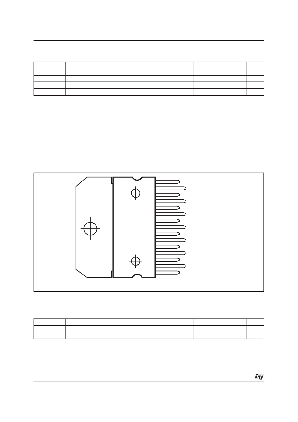
PIN CONNECTION (Top view)
DC Supply Voltage 40 V
Total Power Dissipation (Tamb = 70°C) 20 W
Ambient Operating Temperature (1) 0 to 70 °C
Storage and Junction Temperature -40 to 150 °C
15
14
13
12
11
10
9
8
7
6
5
4
3
2
1
D98AU962A
PW_GND
OUTR
V
S
OUTL
PW_GND
MUTE1 (L/R)
MUTE2 (CENTER)
S_GND
SVR
INC
INL
PW_GND_C
OUTC
V
S_C
INC
THERMAL DATA
Symbol Parameter Value Unit
R
th j-case
R
th j-amb
Thermal Resistance Junction-case Typ. = 1.3 Max. = 1.9 °C/W
Thermal Resistance Junction-ambient max 35 °C/W
2/5
TDA7497
ELECTRICALCHARACTERISTICS
(Refer to the test circuitV
= 28V;RL=8Ω,Rg=50Ω,T
S
amb
Symbol Parameter Test Condition Min. Typ. Max. Unit
S
V
q
I
O
V
O_L/R
P
O_C
P
THD Total Harmonic Distortion P
peak L/R
I
peak C
I
Supply Voltage Range 11 35 V
Total Quiescent Current 100 mA
Quiescent Output Voltage 12.5 14 15.5 V
Output Power Left / Right
Channels
THD= 10%;RL=8Ω;VS= 28V 10 12 W
THD= 1%;R
THD= 10%;R
THD= 1%;R
THD= 10%;R
THD= 1%;R
=8Ω;VS=28V 7.8 9.3 W
L
=4Ω;VS=20V 7 8 W
L
=4Ω;VS=20V 5 6 W
L
=8Ω;VS= 18V 3.5 3.8 W
L
=8Ω;VS=18V 2.2 2.9 W
L
Output Power Center Channel THD = 10%;RL=6Ω;VS= 28V 15 17 W
THD= 1%;R
= 1W; f = 1KHz; 0.4 %
O
=6Ω;VS=28V 11.7 13.3 W
L
Output Peak Current (internally limited) 1.7 2.4 A
Output Peak Current Central
(internally limited) 2 2.8 A
Channel
V
G
Closed Loop Gain 29 30 31 dB
BW 0.6 MHz
N
e
Total Output Noise f= 20Hz to 22KHz 60 150 µV
SR Slew Rate 5 8 V/µs
i
R
SVR Supply Voltage Rejection f = 1kHz
T
M
s
T
Input Resistance 22.5 30 KΩ
35 39 dB
C
SVR
= 470µF; V
RIP
=1V
rms
Thermal Muting 150 °C
Thermal Shut-down 160 °C
MUTE STAND-BY & INPUT SELECTION FUNCTIONS
MUTE1
V
MUTE2
V
MUTE
A
muteBIAS
I
Mute Threshold (L/R) 2.3 2.5 2.7 V
Mute Threshold (Center only) 2.3 2.5 2.7 V
Mute Attenuation 50 65 dB
Mute bias current
Mute1/Mute2
Mute 1 5 µA
Play 0.2 2 µA
=25°C)
3/5

TDA7497
DIM.
MIN. TYP. MAX. MIN. TYP. MAX.
A5
B 2.65 0.104
C 1.6 0.063
D 1 0.039
E 0.49 0.55 0.019 0.022
F 0.66 0.75 0.026 0.030
G 1.02 1.27 1.52 0.040 0.050 0.060
G1 17.53 17.78 18.03 0.690 0.700 0.710
H1 19.6 0.772
H2 20.2 0.795
L 21.9 22.2 22.5 0.862 0.874 0.886
L1 21.7 22.1 22.5 0.854 0.870
L2 17.65 18.1 0.695 0.713
L3 17.25 17.5 17.75 0.679 0.689 0.699
L4 10.3 10.7 10.9 0.406 0.421 0.429
L7 2.65 2.9 0.104 0.114
M 4.25 4.55 4.85 0.167 0.179 0.191
M1 4.63 5.08 5.53 0.182 0.200 0.218
S 1.9 2.6 0.075 0.102
S1 1.9 2.6 0.075 0.102
Dia1 3.65 3.85 0.144 0.152
mm inch
0.197
0.886
OUTLINE AND
MECHANICAL DATA
Multiwatt15 V
4/5

TDA7497
Information furnished is believed to be accurate and reliable. However, STMicroelectronics assumes no responsibility for the consequences
of use of such information nor for any infringement of patents or other rights of third parties which may result from its use. No license is
granted by implication or otherwise under any patent or patent rights of STMicroelectronics. Specification mentioned in this publication are
subject to change without notice. This publication supersedes and replaces all information previously supplied. STMicroelectronics products
are not authorized for use as critical components in life support devices or systems without express written approval of STMicroelectronics.
The ST logo is a registered trademark of STMicroelectronics
2000STMicroelectronics – Printed in Italy– All Rights Reserved
STMicroelectronics GROUP OF COMPANIES
Australia - Brazil - China- Finland- France - Germany - Hong Kong - India - Italy - Japan - Malaysia - Malta - Morocco -
Singapore - Spain - Sweden - Switzerland - United Kingdom - U.S.A.
http://www.st.com
5/5
 Loading...