


2W+2W AMPLIFIER WITH DC VOLUME CONTROL
2W+2W OUTPUT POWER
R
= 8Ω @THD = 10% VCC = 14V
L
ST-BY AND MUTE FUNCTIONS
LOW TURN-ON TURN-OFF POP NOIS E
LINEAR VOLUME CONTROL DC COUPLED
WITH POWER OP. AMP.
NO BOUCHEROT CELL
NO ST-BY RC INPUT NETWORK
SINGLE SUPPLY RANGING UP TO 15V
SHORT CIRCUIT PROTECTION
THERMAL OVERLOAD PROTECTION
INTERNALLY FIXED GAIN
SOFT CLIPPING
VARIABLE OUTPUT AFTER VOLUME CON-
TROL CIRCUIT
POWERDIP (14+3+3) PACKAGE
DESCRIPTION
The TDA7496L is a stereo 2W+2W class AB
power amplifier assembled in the @ Powerdip
TDA7496L
Powerdip (14+3+3)
ORDERING NUMBER:
14+3+3 package, specially designed for high
quality sound, TV and Monitor applications.
Features of the TDA7496L include linear volume
control, Stand-by and mute functions.
TDA7496L
BLOCK DIAGRAM
GND
INR
470nF
INL
470nF
SVR 10
470µF
1,2,3,13,
18,19,20
9
4
30K
VOLUME
100nF
VAROUT_R
VOLUME
VOLUME
65
VAROUT_L
300K
V
S
7
15,16
+
OP AMP
MUTE/STBY
PROTECTIONS
+
-30K
OP AMP
+5V
60K
14
OUTR
11
STBY
12
MUTE
17
OUTL
D97AU596A
1000µF
1000µF
1µF
10K
S1 ST-BY
S2 MUTE
+5V
S_GND
+5V
April 1998
1/10
TDA7496L
ABSOLUTE MAXIMUM RATINGS
Symbol Parameter Value Unit
V
S
V
IN
P
tot
T
amb
T
, T
stg
V
6
DC Supply Voltage 26 V
Maximum Input Voltage 8 Vpp
Total Power Dissipation (T
= 60°C) 6 W
case
Ambient Operating Temperature 0 to 70 °C
Storage and Junction Temperature -40 to 150 °C
j
Volume CTRL DC voltage 7 V
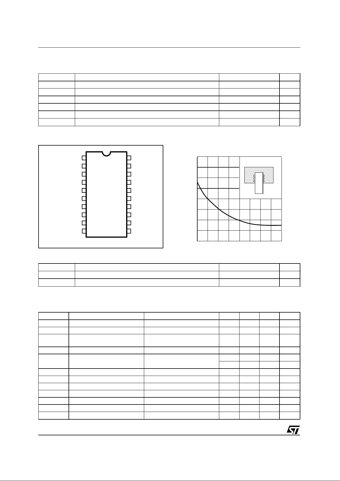
PIN CONNECTION
Rth with "on board" Square Heatsink vs. copper area.
R
GND
GND
GND
INL
VAROUT_L
VOLUME
VAROUT_R
N.C.
INR
1
2
3
4
5
6
7
8
9 MUTE
19
18
17
16
15
14
13
12
GND20
GND
GND
OUTL
V
S
V
S
OUTR
GND
thj-a
(˚C/W)
60
50
40
COPPER AREA 35µ
THICKNESS
D97AU675
PC BOARD
SVR 10 STBY11
D97AU597A
30
0 4 8 12 Area(cm2)
THERMAL DATA
Symbol Parameter Value Unit
R
th j-pins
(*) Thermal Resistance Junction-ambient max. 50 °C/W
R
th j-amb
(*) Mounted on PCB with no heatsink
Thermal Resistance Junction-pins max. 15 °C/W
ELECTRICAL CHARACTERISTICS
(Refer to the te s t ci r cui t V
= 14V; RL = 8Ω, Rg = 50Ω, T
S
= 25°C).
amb
Symbol Parameter Test Condition Min. Typ. Max. Unit
V
DCV
S
I
q
Supply Voltage Range 10 18 V
Total Quiescent Current 25 50 mA
Output DC Offset Referred to
OS
No Input Signal 200 mV
SVR Potenial
V
O
P
O
THD Total Harmonic Distortion G
I
peak
V
in
G
V
G
vLine
A
Min VOL
Quiescent Output Voltage 7 V
Output Power THD = 10%; RL = 8Ω; 1.6 2 W
THD = 1%; R
= 30dB; PO = 1W; f = 1KHz; 0.4 %
V
= 8Ω; 1.3 W
L
Output Peak Current (internally limited) 0.7 0.9 A
Input Signal 2.8 Vrms
Closed Loop Gain Vol Ctrl > 4.5V 28.5 30 31.5 dB
Monitor Out Gain Vol Ctrl > 4.5V; Zload > 30KΩ -1.5 0 1.5 dB
Attenuation at Minimum Volume Vol Ctrl < 0.5V 80 dB
BW 0.6 MHz
2/10
TDA7496L
ELECTRICAL CHARACTERISTICS
(continued)
Symbol Parameter Test Condition Min. Typ. Max. Unit
e
N
Total Output Noise f = 20Hz to 22KHz
500 800 µV
Play, max volume
f = 20Hz to 22KHz
100 250 µV
Play, max attenuation
f = 20Hz to 22KHz
60 150 µV
Mute
SR Slew Rate 5 8 V/µs
R
R
Var Out
R
load Var Out
SVR Supply Voltage Rejection f = 1kHz; max volume
T
M
T
s
Input Resistance 22.5 30 KΩ
i
Variable Output Resistance 30 100 Ω
Variable Output Load 2 KΩ
35 39 dB
C
= 470µF; V
SVR
f = 1kHz; max attenuation
C
= 470µF; V
SVR
RIP
RIP
= 1V
=1V
rms
55 65 dB
rms
Thermal Muting 150 °C
Thermal Shut-down 160 °C
MUTE STAND-BY & INPUT SELECTION FUNCTION S
V
ST ON
V
ST OFF
V
M ON
V
M OFF
I
qST-BY
A
MUTE
I
stbyBIAS
muteBIAS
I
Stand-by ON Threshold 3.5 V
Stand-by OFF Threshold 1.5 V
Mute ON Threshold 3.5 V
Mute OFF Threshold 1.5 V
Quiescent Current @ Stand-by 0.6 1 mA
Mute Attenuation 50 65 dB
Stand-by bias current Stand by on V
V
ST-BY
MUTE
= 5V
= 5V
80 µA
Play or Mute -20 -5 µA
Mute bias current Mute 1 5 µA
Play 0.2 2 µA
µA
APPLICATION SUGGES TION S
The recommended values of the external components are those shown on the application circuit of figure 1A. Different values can be used, the following table can help the designer.
COMPONENT
SUGGESTION
VALUE
R1 300K Volume control
circuit
PURPOSE
LARGER THAN
SUGGESTION
Larger volume regulation
time
R2 10K Mute time constant Larger mute on/off time Smaller mute on/off time
P1 50K Volume control
circuit
C1 1000µF Supply voltage
bypass
C2 470nF Input DC decoupling Lower low frequency cutoff Higher low frequency cutoff
C3 470nF Input DC decoupling Lower low frequency cutoff Higher low frequency cutoff
C4 470µF Ripple rejection Better SVR Worse SVR
C5 100nF Volume control time
costant
C6 1000µF Output DC
Larger volume regulation
time
Lower low frequency cutoff Higher low frequency cutoff
decoupling
C7 1µF Mute time costant Larger mute on/off time Smaller mute on/off time
C8 1000µF Output DC
Lower low frequency cutoff Higher low frequency cutoff
decoupling
C9 100nF Supply voltage
bypass
SMALLER THAN
SUGGESTION
Smaller volume regulation
time
Danger of oscillation
Smaller volume regulation
time
Danger of oscillation
3/10
TDA7496L
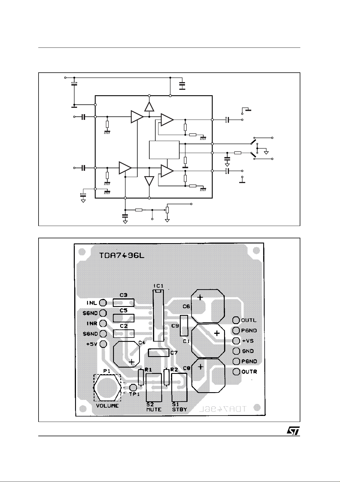
Figure 1A. Application Circuit.
+V
S
C4 470µF
INR
INL
C1
1000µF
PW_GND
C2 470nF
C3 470nF
SVR 10
1,2,3,13,
18,19,20
9
4
30K
VOLUME
C5
100nF
VAROUT_R
VOLUME
VOLUME
65
VAROUT_L
R1 300K
TP1
7
15,16
+
OP AMP
MUTE/STBY
PROTECTIONS
+
-30K
OP AMP
V
VOL
P1
50K
LOG
C9
0.1µF
S
60K
+5V
C8 1000µF
14
11
12
C7
1µF
17
C6 1000µF
R2 10K
D97AU598A
PW_GND
OUTR
OUTL
PW_GND
S1 STBY
S2 MUTE
+5V
S_GND
+5V
Figure 1B. PCB and Component Layout of the Fig. 1A (1.25:1 scale)
4/10

MUTE STAND-BY TRUTH TABLE
MUTE ST-BY OPERATING CONDITION
H H STANDBY
L H STANDBY
H L MUTE
L L PLAY
Turn ON/OFF Sequences (for optimizing the POP performances)
A) USING MUTE AND STAND-BY FUNCTION S
VS (V)
ST-BY
pin#11 (V)
5
TDA7496L
V
SVR
pin#10(V)
2.5V
MUTE
pin#12 (V)
5
INPUT
(mV)
V
OUT
(V)
I
Q
(mA)
OFFSTBY MUTE PLAY STBYOFF MUTE
D97AU683
B) USING ONLY THE MUTE FUNCTI ON
To simplify the application, the stand-by pin can
be connected directly to Ground.
During the ON/OFF transitions is recommend to
respect the following conditions.
- At the turn-on, the transition mute - play must be
made when the SVR pin is higher than 2.5V
- At the turn-off, t he TDA7496L must be brought
to mute from the play condition when the SVR pin
is higher than 2.5V.
5/10

TDA7496L
Quiescent current vs. Supply Voltage
Iq (mA)
34
32
30
28
26
24
22
20
18
16
Vi=0
10 11 12 13 14 15 16 17 18
Supply Vol tage (V)
Output DC Offset vs. Supply Voltage
Vodc-Vs v r (V)
300
280
260
240
220
200
180
160
140
120
100
10 11 12 13 14 15 16 17 18
Vi=0
Supply Vol tage (V)
Output DC Voltage vs. Supply Voltage
Vodc (V)
10
9.5
9
8.5
8
7.5
7
6.5
6
5.5
5
4.5
4
Vi=0
10 11 12 13 14 15 16 17 18
Supply Vol tage (V)
Output Power vs. Supp ly Voltage
Oup ut Powe r (W)
4
3.5
3
2.5
2
1.5
1
0.5
0
Rl=8 Ohm
F= 1 KHz
10 11 12 13 14 15 16 17 18
Supply Vol tage (V)
THD=10 %
THD=1 %
Distortion vs. Output Power
Distortion (%)
10
Vs=12V
Rl=8 Ohm
1
0.1
F=1 KHz
0.01
0 0.2 0.4 0 .6 0.8 1 1.2 1 .4 1.6 1 .8 2
Output Power (W)
6/10
F=15 KHz
Closed Loop gain vs. Frequency
Closed Loop Gain (dB)
32
31
30
29
28
27
26
25
24
23
22
21
20
0.02 0.2 2 20
Frequency (KHz)
Rl=8 Ohm
Pout=0.5W
Cin=470nF
Cout =1000uF
Csvr=470 uF

TDA7496L
St-By Atten u ati on vs . Vpi n 11
Stand-by Attenuation (dB)
20
10
0
-10
-20
-30
-40
Rl=8 Ohm
-50
0 dB @ Pout=1W
-60
-70
-80
-90
-100
-110
-120
-130
-140
00.511.522.533.544.55
Vpin # 11 (V)
PIN DESCRIPTION
Mute Attenuation vs. Vpin 12
Mute Att enu ation (dB)
20
10
0
-10
-20
-30
Rl=8 Ohm
-40
0 dB @ Pout=1W
-50
-60
-70
-80
-90
-100
-110
-120
0 0.4 0.8 1.2 1.6 2 2.4 2.8 3.2 3.6 4 4.4 4.8 5.2
Vpin # 12 (V)
PIN: SVR
SVR
V
S
20K
20K
100µA
V
S
V
S
+
OUT L
-
6K
6K
1K
1K
30K
30K
-
OUT R
+
D97AU585A
7/10

TDA7496L
PINS: INL, INR
INn
SVR
PIN: VOLUME
VOL
30K
10µA
D97AU591
6K
D97AU589
V
S
V
S
500µA
PINS: VAROUT-L, VAROUT-R
V
S
VAROUT-L
D97AU590
PIN: MUTE
200MUTE
10K
D97AU592
50µA
V
S
PINS: PW-GND, S-GND
GND
PIN: STBY
STBY
200
65K
V
D97AU593
PINS: OUT R, OUT L
V
S
S
D97AU588
V
S
10µA
OUT
8/10
D97AU594

POWERDIP20 PACKAGE MECHA NICAL DATA
TDA7496L
DIM.
MIN. TYP. MAX. MIN. TYP. MAX.
a1 0.51 0.020
B 0.85 1.40 0.033 0.055
b 0.50 0.020
b1 0.38 0.50 0.015 0.020
D 24.80 0.976
E 8.80 0.34 6
e 2.54 0.100
e3 22.86 0.900
F 7.10 0.280
I 5.10 0.201
L 3.30 0.130
Z 1.27 0.050
mm inch
9/10

TDA7496L
Information furnished is believed to be acc urate and reliable. However, SGS-THOMSON Microelectronics assumes no responsibility for the
consequences of us e of s uch information nor for any i nfringement of patents or other right s of third part ie s whi ch may result from its use. No
license is granted by implication or otherwise under any patent or patent r ights of SGS-THOMSO N Microelectroni cs. Specification me ntioned in this publication are sub ject to change wit hout notice. This publication su persedes and replaces all information previ ously supp lied.
SGS-THOMSON Mic roelectr onics produc ts are not authorized f or use as critical components in life sup port devic es or sy stems wit hout express written approval of SGS-THOMSON Microelectronics.
© 1998 SGS-THOMSON Microelectronics – Printed in Italy – All Rights Reserved
SGS-THOMSON Microelectronics GROUP OF COMPANIES
Australia - Brazil - Canada - China - France - Germany - Italy - Japan - Korea - Malaysia - Malta - Morocco - The Netherlands -
Singapore - Spain - Sweden - Switzerland - Taiwan - Thailand - United Kingdom - U.S.A.
10/10
 Loading...