

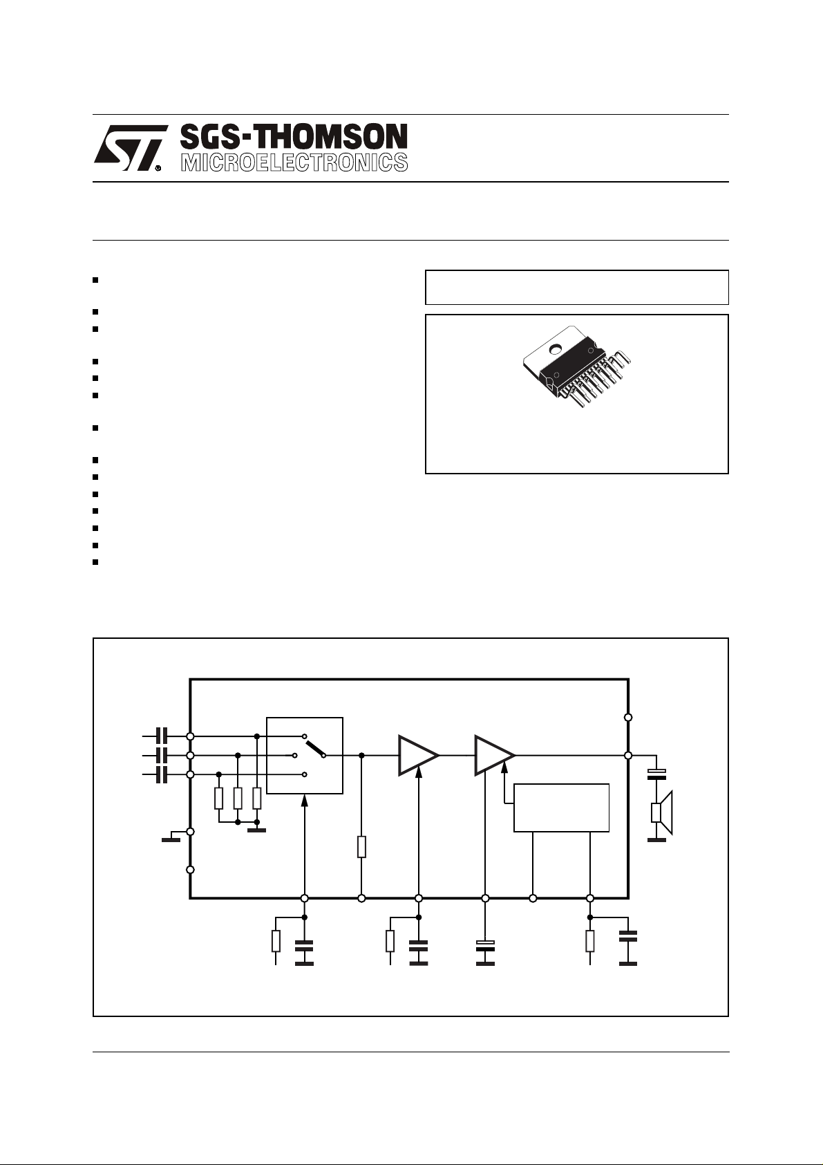
TDA7494
10W AMPLIFIER WITH DC VOLUME CONTROL
10W OUTPUT POWER RL = 8Ω,
@ THD = 10% V
CC
= 28V
ST-BY AND MUTE FUNCTIONS
LINEAR VOLUME CONTROL DC COUPLED
WITH POWER OP AMPLIFIER
NO BOUCHEROT CELL
NO ST-BY RC INPUT NETWORK
SIGNAL LINE OUTPUT BEFORE VOLUME
CONTROLLING AND MUTING
3 SWITCHABLE VOLTAGE CONTROLLED
INPUT PINS
SINGLE SUPPLY RANGING UP TO 35V
SHORT CIRCUIT PROTECTION
THERMAL OVERLOAD PROTECTION
INTERNALLY FIXED GAIN
SOFT CLIPPING
LOW TURN-ON TURN-OFF POP NOIS E
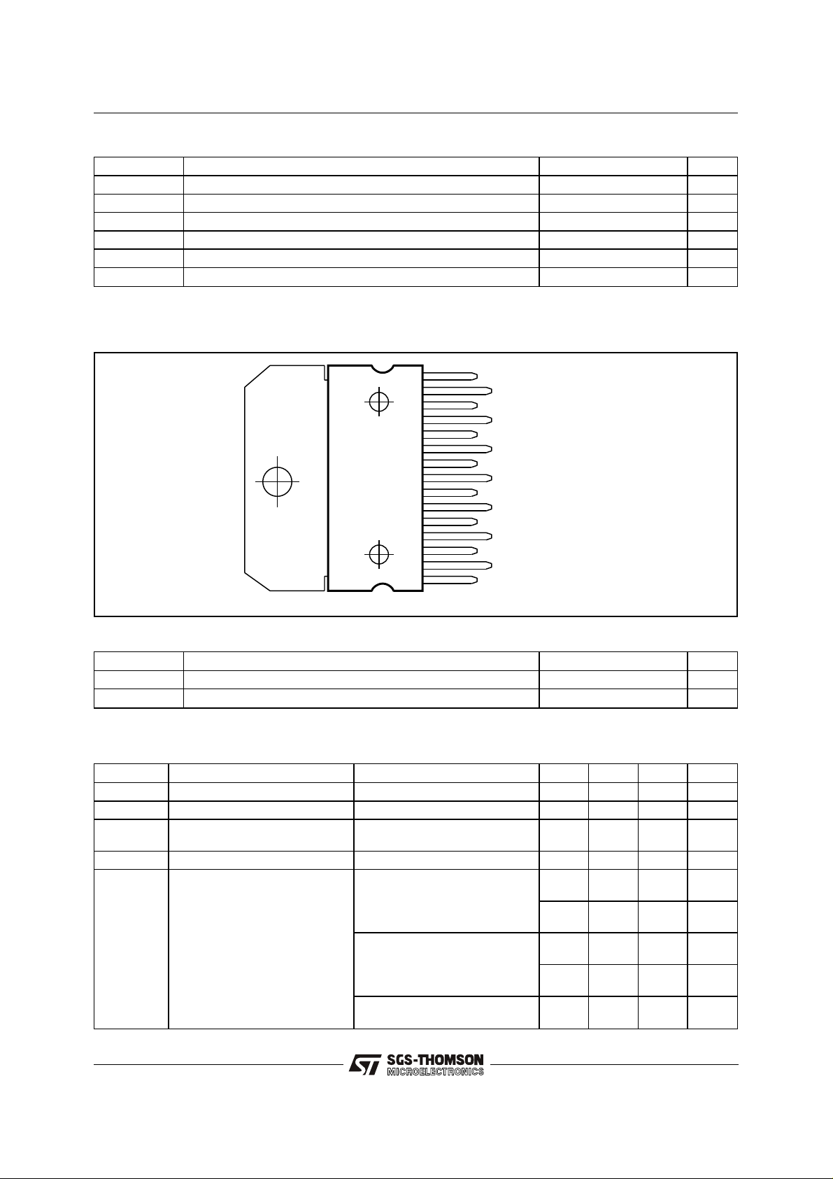
MULTIWATT 15 PACKAGE
BLOCK AND APPLICATION DIAGRAM
MULTIPOWER BI50II TECHNOLOGY
Multiwatt15
ORDERING NUMBER:
DESCRIPTION
The TDA7494 10W is class AB power amplifier
assembled in the @Multiwatt 15 package, specially designed for high quality sound, TV applications.
Features of the TDA7494 include volume control,
3 switchable inputs, Stand-by and mute functions.
TDA7494
3 x
470nF
IN 1
IN 2
IN 3
PWR GND
SGN GND
February 1997
5
6
1
15
8
D95AU414D
100K
2
SW CTL
SW
1
3
243 7910
MONITOR
OUT
100K
300nF
VOL PWR
2K
VOL CTL
300nF
SVR
MUTE/STBY
PROTECTIONS
STAND-BY
470µF
10K 1µF
13 +V
14
MUTE
CC
470µF
OUT
1/12
TDA7494
ABSOLUTE MAXIMUM RATINGS
Symbol Parameter Value Unit
V
S
V
IN
P
tot
T
amb
, T
T
stg
, V
V
2
(1) Operation between -20 to 85 °C guaranteed by correlation with 0 to 70°C.
PIN CONNECTION
DC Supply Voltage 35 V
Maximum Input Voltage 8 Vpp
Total Power Dissipation (Tamb = 70°C) 16 W
Ambient Operating Temperature Range (1) -20 to +85 °C
Storage and Junction Temperature -40 to 150 °C
j
Volume CTRL DC voltage 7 V
3
D95AU415A
PWR GND
OUT
+V
CC
N.C.
N.C.
MUTE
STAND-BY
SGN GND
SVR
IN 2
IN 1
MONITOR OUT
VOLUME CONTROL
SW CTL
IN 3
15
14
13
12
11
10
9
8
7
6
5
4
3
2
1
THERMAL DATA
Symbol Parameter Value Unit
R
th j-case
R
th j-amb
ELECTRICAL CHARACTERISTICS
= 25°C; unless otherwise specified.)
T
amb
Symbol Parameter Test Condition Min. Typ. Max. Unit
V
S
I
q
DCV
OS
V
O
P
O
Thermal Resistance Junction-case Typ = 3.8 Max = 4.8 °C/W
Thermal Resistance Junction-ambient max 35 °C/W
(Refer to the test circuit, V
= 21V, RL = 8Ω; Rg = 50Ω;
S
Supply Voltage Range 11 35 V
Total Quiescent Current 22 50 mA
Output DC Offset Referred to
No Input Signal -400 400 mV
SVR Potential
Quiescent Output Voltage VS = 28V 14 V
Output Power THD = 10%; VCC = 28V, RL = 8Ω
THD = 1%; V
CC
= 28V
THD = 10%; VCC = 21V,
THD = 1%; V
THD = 10%; V
THD = 1%; V
= 21V,
CC
= 21V, RL = 4Ω
CC
= 21V,
CC
THD = 10%; VCC = 18V,
THD = 1%; V
THD = 10%; V
THD = 1%; V
= 18V
CC
= 18V, RL = 8Ω
CC
= 18V
CC
8
6
5
3.5
5
3.9
4.5
3.5
3.5
2.5
10
8
5.5
4
7.5
5.5
6
4.5
3.75
2.85
W
W
W
W
W
W
2/12
TDA7494
ELECTRICAL CHARACTERISTICS
(continued)
Symbol Parameter Test Condition Min. Typ. Max. Unit
THD Total Harmonic Distortion P
I
G
A
MinVol
peak
T
V
G
vLine
op
in
V
Output Peak Current (internally limited) 1.4 1.9 A
Operating Temperature 0 70 °C
Input Signal 2.8 Vrms
Closed Loop Gain Vol Ctrl > 4.5V 24.5 26 27.5 dB
Monitor Out Gain R
Attenuation at Min Volume Vol Ctrl < 0.5V 80 dB
= 1W; f = 1KHz; Gv = 26dB 0.4 %
O
LOAD Mon
= ∞ -3 -1.5 0 dB
BW 0.6 MHz
e
N
Total Output Noise f = 20Hz to 22KHz
350 700 µV
Play, max volume
f = 20Hz to 22KHz
60 100 µV
Play, max attenuation
f = 20Hz to 22KHz
30 50 µV
Mute
SR Slew Rate 5 8 V/µs
R
i
R
Mon
R
load Mon
SVR Supply Voltage Rejection f = 1kHz; max volume
T
M
T
s
V
ST-BY
V
MUTE
Input Resistance 22.5 30 KΩ
Monitor Output Resistance 1.4 2 3 KΩ
Monitor Output Load 30 KΩ
36 43 dB
C
= 470µA; V
SVR
f = 1kHz; max attenuation
C
= 470µA; V
SVR
RIP
RIP
= 1V
= 1V
RMS
60 73 dB
RMS
Thermal Muting 150 °C
Thermal Shut-down 160 °C
Stand-by threshold 2.3 2.5 2.7 V
Mute Threshold 2.3 2.5 2.7 V
Sel #1 Control Voltage Input #1 selected 0 1 V
Sel #2 Control Voltage Input #2 selected 2.3 2.7 V
Sel #3 Control Voltage Input #3 selected 4 5 V
I
qST-BY
A
MUTE
I
stbyBIAS
Quiescent Current @ Stand-by 0.6 1 mA
Mute Attenuation 60 75 dB
Stand-by bias current Stand by on; V
V
= 5V;
MUTE
ST-BY
= 5V;
80 150 µA
Play or Mute 2 20 µA
I
muteBIAS
Mute bias current Mute 1.5 10 µA
Play 0.5 5 µA
I
switchBIAS
Switch bias current Input #1 selected -0.5 5 µA
Input #2 selected 1 10 µA
Input #3 selected 1.5 20 µA
3/12
TDA7494
Figure 1:
+5V
R1
3.3K
R2
3.3K
Figure 2:
Test and Application Circuit.
MONITOR
OUT
213
IN 1
IN 2
IN 3
C3 470nF
C4 470nF
C5 470nF
S1
4
JMP1
TP1
4
5
6
1
R3 100K
300nF
C6
SGN GND
P.C.B. and component layout.
13 +V
SW
1
2
3
82
+5V
VOL
P1
50K
LOG
R4
100K
5K
VOL PWR
TP2
C10 470µF
14
MUTE/STBY
PROTECTIONS
37910
SVR
C7
300nF
C8
470µF
STAND-
BY
R5
10K
S3S2
15
MUTE
GND
C9
1µF
+5V
+5V
D96AU492B
C2
0.1µF
OUT
PGND
C1
1000µF
GND
CC
4/12

TDA7494
APPLICATION SUGGES TION S
The recommended values of t he external components are those shown on t he application circuit of figure 1. Different values can be used; the following table can help the designer.
COMPONENT
R1 3.3KΩ Input switch circuit Vpin #2 shifted downward Vpin #2 shifted upward
R2 3.3KΩ Input switch circuit Vpin #2 shifted upward Vpin #2 shifted downward
R3 100KΩ
R4 100KΩ
R5 10KΩ Mute time constant Larger mute on/off time Smaller mute on/off time
P1 50KΩ Volume control circuit
C1 1000µF Supply voltage bypass Danger of oscillation
C2 100nF Supply voltage bypass Danger of oscillation
C3 470nF Input DC decoupling
C4 470nF Input DC decoupling
C5 470nF Input DC decoupling
C6 300nF
C7 300nF
C8 470µF Ripple Rejection Better SVR Worse SVR
C9 1µF Mute time constant Larger mute on/off time Smaller mute on/off time
C10 470µF Output DC decoupling
SUGGESTION
VALUE
PURPOSE
Input switch time
constant
Volume control time
constant
Input- switch time
constant
Volume control time
constant
LARGER THAN
SUGGESTION
Larger Input Switch Time Smaller input switch time
Larger Volume
Regulation Time
Lower low frequency
cutoff
Lower low frequency
cutoff
Lower low frequency
cutoff
Larger-Input- switch time Smaller input- switch time
Larger volume regulation
time
Lower low frequency
cutoff
SMALLER THAN
SUGGESTION
Smaller volume
regulation time
Higher low frequency
cutoff
Higher low frequency
cutoff
Higher low frequency
cutoff
Smaller volume regulation
time
Higher low frequency
cutoff
TYPICAL CHARACTERISTICS:
Refer to the Application Circuit of Fig.1 V
RS = 8Ω; Tamb = 25°C; RS = 50Ω; unless otherwise specified
Figure 3:
P
Output Power vs Supply Voltage
OUT
(W)
14
12
10
8
6
4
2
0
5 10 15 20 25 30 Vs(V)
d=10%
D96AU517
d=1%
Figure 4:
d
(%)
1
0.1
0.01
= 21V; RL = 8Ω; f = 1KHz;
S
Distortion vs Output Power
D96AU518
VS=28V
R
=8Ω
L
f=15KHz
f=1KHz
02468P
OUT
(W)
5/12

TDA7494
Figure 5:
P
OUT
(W)
7
6
5
4
3
2
1
0
11 13 15 17 19 VS(V)
Figure 7:
d
(%)
1
Output Power vs Supply Voltage
D96AU519
RL=4Ω
d=10%
d=1%
Distortion vs Frequency
D96AU521
P
=1W
OUT
R
=8Ω
L
Figure 6:
d
(%)
1
0.1
0.01
0246P
Figure 8:
d
(%)
1
Distortion vs Output Power
VS=21V
=4Ω
R
L
f=15KHz
f=1KHz
Distortion vs Frequency
P
=1W
OUT
=4Ω
R
L
D96AU520
OUT
D96AU522
(W)
0.1
0.01
20
Figure 9:
I
Q
(mA)
28
26
24
22
20
18
16
10 14 18 22 26 30 VS(V)
100
1K
f(Hz)
Quiescent Current vs Supply Voltage
D96AU523
0.1
0.01
20
Figure 10:
V
DDC
(V)
15
13
11
9
7
5
10 14 18 22 26 30 VS(V)
100
1K
f(Hz)
Quiescent Output Voltage vs Supply
Voltage
D96AU524
6/12

TDA7494
Figure 11:
Gain vs Volume Control (pin #3)
Gain
(dB)
20
10
0
-10
P
OUT
=1W
-20
-30
-40
-50
-60
-70
-80
-90
0.0 1.0 2.0 3.0 4.0 Vpin#3(V)
Figure 13:
ATT
(dB)
-20
-40
Stand-by Attenuation vs Vpin # 9
0
0dB=1W
D96AU525
D96AU527
Figure 12:
Supply Voltage Rejection vs Fre-
quency
SVR
(dB)
V
=1V
RIP
-20
-40
-60
-80
-100
20 100 1K f(Hz)
Figure 14:
ATT
(dB)
0
-20
MAX VOLUME
MAX ATTENUATION
Mute Atttenuation vs Vpin # 10
RMS
0dB=1W
D96AU526
D96AU528
-60
-80
-100
-120
-140
0 1 2 3 4 Vpin#9(V)
Figure 15:
P
DISS
(W)
8
6
4
2
Power Dissipation vs Output Power
D96AU529
RL=8Ω
VS=35V
VS=28V
VS=21V
-40
-60
-80
-100
01234Vpin#10(V)
Figure 16:
P
DISS
(W)
8
6
4
2
Power Dissipation vs Output Power
D96AU530
RL=4Ω
VS=21V
VS=18V
0
0.1 1 10 P
OUT
(W)
0
0.1 1 10 P
OUT
(W)
7/12

TDA7494
MUTE STAND-BY TRUTH TABLE
MUTE ST-BY OPERATING CONDITION
H H STANDBY
L H STANDBY
H L MUTE
L L PLAY
Turn ON/OFF Sequences (for optimising the POP performances)
A) USING MUTE AND STAND-BY FUNCTION S
(V)
V
S
28
ST-BY
pin#9 (V)
5
V
SVR
pin#7(V)
2.5V
MUTE
pin#10 (V)
5
INPUT
(mV)
V
OUT
(V)
I
Q
(mA)
B) USING ONLY THE MUTE FUNCTI ON
To semplify the application, the stand-by pin can
be connected directly to Ground.
During the ON/OFF tr ansitions we recommend to
respect the following conditions:
OFFSTBY MUTE PLAY STBYOFF MUTE
D96AU531A
- At the turn-on the transition mute to play must
be made when the SVR pin is higher than
2.5V
- At the turn-off the TDA7494 must be brought
to mute from the play condition when the SVR
pin is higher than 2.5V.
8/12

TDA7494
PINS:
IN3, IN1, IN2
PIN:
VOLUME
INn
SVR
D97AU581
VOL
30K
10µA
D97AU591
V
V
S
S
100µA
PIN:
SWITCH
PIN:
MONITOR
SWITCH
D97AU582
BUFFER
2K
V
S
10µA
MONITOR
V
S
10µA
D97AU584
PIN:
SVR
SVR
1mA
V
V
S
S
V
S
V
S
+
OUT L
-
20K
20K
6K
6K
1K
1K
30K
30K
-
OUT R
+
100µA
D97AU585
9/12

TDA7494
PIN:
ST-BY
PIN:
MUTE
PIN:
OUT
STBY
D97AU588
200
10µA
D97AU586
V
OUT
V
S
300MUTE
10K
V
S
50µA
D97AU587
PINS:
PW-GND , S-G ND
S
V
S
GND
D97AU593
10/12

MULTIWATT15 PACKAGE MECHANICAL DATA
TDA7494
DIM.
MIN. TYP. MAX. MIN. TYP. MAX.
A 5 0.197
B 2.65 0.104
C 1.6 0.063
D 1 0.039
E 0.49 0.55 0.019 0.022
F 0.66 0.75 0.026 0.030
G 1.02 1.27 1.52 0.040 0.050 0.060
G1 17.53 17.78 18.03 0.690 0.700 0.710
H1 19.6 0.772
H2 20.2 0.795
L 21.9 22.2 22.5 0.862 0.874 0.886
L1 21.7 22.1 22.5 0.854 0.870 0.886
L2 17.65 18.1 0.695 0.713
L3 17.25 17.5 17.75 0.679 0.689 0.699
L4 10.3 10.7 10.9 0.406 0.421 0.429
L7 2.65 2.9 0.104 0.114
M 4.25 4.55 4.85 0.167 0.179 0.191
M1 4.63 5.08 5.53 0.182 0.200 0.218
S 1.9 2.6 0.075 0.102
S1 1.9 2.6 0.075 0.102
Dia1 3.65 3.85 0.144 0.152
mm inch
11/12

TDA7494
Information furnis hed is believe d to be ac curate and reliabl e. However, SGS-THOMS ON Mi croelect ronics as sumes no res ponsib ility for the
consequences of use of such information nor for any infringement of patents or othe r ri ghts of third parties w hi ch m ay result from i ts use. No
license is granted by implication or otherwise under any patent or patent rights of SGS-THOMSON Microelectronics. Specification me ntio ned
in this publication are subject to change without notice. This publication supersedes and replaces all information previously supplied.
SGS-THOMSON Microelectronics products are not authorized for use as critical components in life support devices or systems without express
written approval of SGS-THOMSON Microelectronics.
© 1997 SGS-THOMSON Microelectronics – Printed in Italy – All Rights Reserved
SGS-THOMSON Microelectronics GROUP OF COMPANIES
Australia - Brazil - Canada - China - France - Germany - Hong Kong - Italy - Japan - Korea - Malaysia - Malta - Morocco - The Netherlands -
Singapore - Spain - Sweden - Switzerland - Taiwan - Thailand - United Kingdom - U.S.A.
12/12
 Loading...