


®
25W + 25W STEREO CLASS-D AMPLIFIER
25W + 25W OUTPUT POWER:
R
= 8Ω/4
L
HIGH EFFICIENCY
WIDE SUPPLY VOLTAGE RANGE (FROM
10 TO ±25V)
±
SPLIT SU PPLY
TURN OFF/ON POP FREE
ST-BY AND MUTE F EA T U RES
SHORT CIRCUIT PROTECTION ACROSS
THE LOAD
THERMAL OVERLOAD PROTECTION
EXTERNALLY SINCHRO NIZABLE
BRIDGE CONFIGURATION
Figure 1. Test and application circuit. (Stereo Configuration)
THD = 10%
Ω;
DESCRIPTION
The TDA7490 is a dual audio class D amplifier
assembled in Flexiwatt 25 package; it is specially
designed for high efficiency application mainly for
TV and Home Stereo sets.
50W MONO IN BTL
Flexiwatt 25
ORDERING NUMBER:
TDA7490
PRODUCT PREVIEW
TDA7490
R1 10K
C3
100nF
C4
100nF
STBYMUTE R2
R3
10K
INPUT1
R1 10K
-V
CC
-V
CC
INPUT2
C1 330nF
C2
1nF
C7 100nF
C5 330nF
C6
1nF
R 6.8
30K
C27
2.2µF
R21 4.7K
10
PREAMPLIFIER1
12
13
16
1
25
PREAMPLIFIER2
G=2.5
18
R5 4.7K
R17 52.3K
+V
C26 470pF C25 470pF
R20
68K
79
INTEGRATOR1
INTEGRATOR2
19 17
C8 470pF
R6
C9 470pF
68K
CC
R4
130K
14 2 46
PWM-stage1G=2.5
PWM-stage2
20 24 22
R9 52.3K
C23
2200µF
OSC
C28
2200µF
+V
-V
-V
CC
CC
C22
C21
100nF
2200µF
5
3
C18 330pF
11
8
C16 330pF
15
23
21
C12
C11
2200µF
100nF
+V
CC
CC
C20
33nF
R14 22K
C17
24pF
R12 22K
C14
33nF
-V
CC
-V
CC
R15
100
C19
560pF
R13
10K
C15
560pF
R11
100
D98AU978A
L1 30µ
L2 30µ
OUT1
C10
220nF
OUT2
C29
220nF
EXT_CK
December 1999
This is preliminary information on a new product now in development. Details are subject to change without notice.
1/9

TDA7490
Figure 2. Test and application circuit. (Bridge Configuration)
INPUT
R63
4.7K
10
PRE +
PRE
18
C41
R5 52.3K
PWM-stage
PWM-stage
R62 52.3K
3
23
470pF 470pF
C40
R4
68K
79
-
Int.
+
Int.
-
19 17
470pF 470pF
C60 C59
R61
68K
The LC filter is optimized for 8Ω
(<->LC filter for 4Ω in single-ended)
It hos to be changed for other loads
L9 30µ
C23
235nF
C24
235nF
L10 30µ
C26
470nF
C29
470nF
D99AU1081
R27
10
R28
10
dumping
(common
mode)
R25
Rload
ABSOLUTE MAXIMUM RATINGS
Symbol Parameter Value Unit
V
P
T
stg
T
V
6,8,10,18
CC
tot
op
, T
DC Supply Voltage (no signal)
Power Dissipation T
Storage and Junction Temperature –40 to 150 °C
j
= 70°C 35 W
case
Operating Temperature Range 0 to 70 °C
Maximum Voltage on pins # 6,8,10,18 referred to GND
30 V
±
5V
±
THERMAL DATA
Symbol Parameter Typ. Max. Unit
R
th j-case
Thermal Resistance Junction-case 1 °C/W
2/9
PIN CONNECTION (Top view)
1 25
TDA7490
-VCC-V
CC
OUT1
CC
+V
BOOT1
OSC
FEED1
STBY-MUTE
IN1
FEED2
T1
+5V
GND
T2
CURREF
PIN FUNCTIONS
N. Name Function
10
11
12
13
14
15
16
17
18
19
20
21
22
23
24
25
1
2
3
4
5
6
7
8
9
-V
CC sign/sub
-V
CCpow1
out 1
+V
CCpow1
BOOT1
STBY-MUTE
FEED1
OSC
FEED2
IN1
T1
+5V
GND
CURREF
T2
-5V
FEED3
IN2
FEED4
NC
BOOT2
+V
CCpow2
OUT2
-V
CCpow2
V
reg
Negative signal/substrate supply
Negative power supply CH1
PWM output of CH1
Positive power supply CH1
Bootstrap CH1
Control State Pin
Feedback pin 1 CH1
Master Oscillator Setting Freequency Pin (or external sync.)
Feedback pin2 CH1
Input CH1
Triangular waveform CH1
+5V regulator (only for internal purposes)
Signal ground
Setting current resistor
Triangular waveform CH2
-5V regulator (only for internal purposes)
Feedback pin1 CH2
Input CH2
Feedback pin2 CH2
Not connected
Bootstrap CH2
Positive power supply CH2
PWM output of CH2
Negative power supply CH2
10V regulator
-5V
IN2
FEED3
N.C.
FEED4
CC
+V
BOOT2
D97AU816B
OUT2
CC
Vreg
-V
3/9

TDA7490
ELECTRICAL CHARACTERISTICS (Refer to the test circuit, V
CC
= ±21V; RL = 8Ω; Demod. filter L =
30mH, C = 220nF; f = 1KHz; fsw = 200kHz; Tamb = 25°‘C unless otherwise specified.)
Symbol Parameter Test Condition Min. Typ. Max. Unit
V
S
I
q
V
OS
P
O
Supply Range
Total Quiescent Current RL = ∞ no LC filter 70 120 mA
Output Offset Voltage –150 +150 mV
Output Power THD = 10%
THD = 1%
P
O(BTL)
Output Power in Bridge
Configuration
Vs =±22V; RL = 16
THD = 10%
Ω
THD = 1%
Vs =±17V; R
= 8
L
Ω
THD = 10%
THD = 1%
(1)
P
O
Output Power RL = 4Ω VCC = ±16V
THD = 10%
THD = 1%
P
D
(2)
η
Maximum Dissipated Power VCC = ±21V; RL = 8
P
= 25W + 25W; THD = 10%
O
Ω
Efficiency (*) PO = 25W + 25W 89 %
THD Total Harmonic Distortion RL = 8Ω; PO = 1W 0.1 %
I
max
Overcurrent Protection
RL = 0 3.5 5 A
Threshold
T
j
Thermal Shut-down Junction
Temperature
G
V
G
∆
V
e
N
C
T
R
i
Closed Loop Gain 30 dB
(3)
Gain Matching -1 +1 dB
Total Input Noise
R
= 50Ω
G
A Curve
f = 20Hz to 22KHz
Cross talk f = 1KHz, PO = 1W 55 dB
Input Resistance 30 k
SVR Supply Voltage Rejection f = 100Hz; Vr = 0.5 60 dB
V
Tr, T
R
DSON
F
SW
rmax
Overvoltage Threshold
Rising and Falling Time 50 ns
f
Power Transistor on Resistance 0.4
(4)
Switching Frequency Range 100 200 230 KHz
(5)
MUTE & STAND-BY FUNCTIONS
V
ST-BY
V
MUTE
V
PLAY
A
MUTE
I
qST-BY
*: PO = measured across the load using the following inductor:
COIL58120 MPPA 2 (magnectics) TURN S = 20 ø 1mm
(1) L = 15µH, C = 470nF
= 90% where VCC = ±25V; RL = 8Ω; PO = 43W + 43W; THD = 20%
(2)
η
Top
(3) ∆Gv is intended with R2, R17, R5, R9 1% precision
= 0.25 ⋅ (1/(300ns + R13 ⋅ ( C17 + 76pF) ⋅ 0.85)
(4) F
SW
(5) V
RMAX
Stand-by range 0 0.7 V
Mute Range 1.7 2.5 V
Play Range 4 5 V
Mute Attenuation 60 dB
Quiescent Current @ Stand-by 3 mA
= (+VCC) - (-VCC) when VR ≥V
RMAX
the device goes in Stand-By mode
10
±
25 V
±
25
18
50
40
50
40
25
18
6W
150 °C
7
12
55 60 V
W
W
W
W
W
W
W
W
V
µ
V
µ
Ω
Ω
4/9

Figure 3. P.C. Board and component layout of the Figs. 1, 2.
(for Stereo and Bridge compatible configuration)
TDA7490
C
O
M
P
O
N
E
N
T
S
I
D
E
S
O
L
D
E
R
S
I
D
E
5/9

TDA7490
Figure 4. Distortion vs. Output Power
THD
(%)
5
2
1
0.5
0.2
0.1
0.05
0.02
0.01
0246 16182022248 101214 PO(W)
Stereo
V
± 21V; Rl=8Ω;
S
f=1KHz
Figure 6. Crosstalk vs. Frequency
CT
(dB)
-20
-30
-40
-50
-60
-70
-80
-90
-100
0.001 0.01 0.1 1 f(KHz)111
VS ± 21V;
Rl=8Ω;
0dB=1W
D99AU1088
D99AU1090
Figure 5. Distortion vs. Output Power
THD
(%)
5
2
1
0.5
0.2
0.1
0.05
0.02
0.01
0246 16182022248 101214 PO(W)
Stereo
V
± 16V; Rl=4Ω;
S
f=1KHz
D99AU1089
Figure 7. Frequency Response
AMP
(dB)
2
0
-2
-4
-6
-8
-10
-12
-14
0.01 0.1 1 10 f(KHz)
VS ± 21V;
Rl=8Ω;
0dB=1W
D99AU1091
Figure 8. Power Dissipation vs. Output Power
Power Dissipation (W)
8
7.5
7
6.5
5.5
4.5
3.5
2.5
1.5
0.5
6/9
Vs= +/- 21 V; Rl = 8 Ohm; f= 1 KHz
6
5
4
3
2
1
0
0 2 4 6 8 10 12 14 16 18 20 22 24 26
Output Power (W)
Figure 9. Distortion vs Output Power in BTL
THD
(%)
5
2
1
0.5
0.2
0.1
0.05
0.02
0.01
0 5 10 15 20 25 30 35 40 45 50 PO(W)
Bridge
V
± 17V;
S
Rl=8Ω;
f=1KHz
D99AU1082

Figure 10. Distortion vs Output Power in BTL
TDA7490
THD
(%)
5
2
1
0.5
0.2
0.1
0.05
0.02
0.01
0 5 10 15 20 25 30 35 40 45 50 PO(W)
Bridge
V
± 22V;
S
Rl=16Ω;
f=1KHz
D99AU1083
7/9

TDA7490
DIM.
MIN. TYP. MAX. MIN. TYP. MAX.
mm inch
A 4.45 4.50 4.65 0.175 0.177 0.183
B 1.80 1.90 2.00 0.070 0.074 0.079
C 1.40 0.055
D 0.75 0.90 1.05 0.029 0.035 0.041
E 0.37 0.39 0.42 0.014 0.015 0.016
F (1) 0.57 0.022
G 0.80 1.00 1.20 0.031 0.040 0.047
G1 23.75 24.00 24.25 0.935 0.945 0.955
H (2) 28.90 29.23 29.30 1.138 1.150 1.153
H1 17.00 0.669
H2 12.80 0.503
H3 0.80 0.031
L (2) 22.07 22.47 22.87 0.869 0.884 0.904
L1 18.57 18.97 19.37 0.731 0.747 0.762
L2 (2) 15.50 15.70 15.90 0.610 0.618 0.626
L3 7.70 7.85 7.95 0.303 0.309 0.313
L4 5 0.197
L5 3.5 0.138
M 3.70 4.00 4.30 0.145 0.157 0.169
M1 3.60 4.00 4.40 0.142 0.157 0.173
N 2.20 0.086
O 2 0.079
R 1.70 0.067
R1 0.5 0.02
R2 0.3 0.12
R3 1.25 0.049
R4 0.50 0.019
V 5˚ (Typ.)
V1 3˚ (Typ.)
V2 20˚ (Typ.)
V3 45˚ (Typ.)
(1): dam-bar protusion not includ ed
(2): molding protusion included
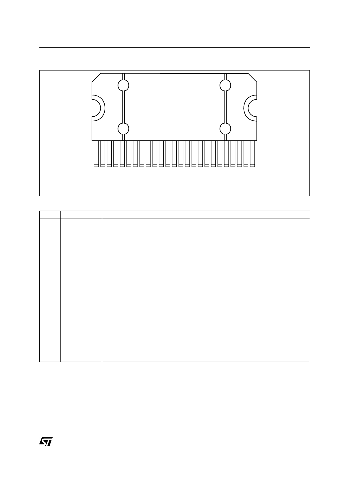
OUTLINE AND
MECHANICAL DATA
Flexiwatt25
L2
H
V3
OL3 L4
V
C
H3
G
H1
G1
R3
H2
F
A
R4
N
V2
R2
R
V
R2
B
L
FLEX25ME
L1
V1
R1
L5
V1
R1 R1
M1
M
D
E
8/9

TDA7490
Information furnishe d is beli eved to be accu rate and reliable. However, STMicroelec tronics assumes no res ponsibility for the consequences
of use of such i nformation nor for any i nfringement of patents or ot her rights of third par ties which may result from its use. No license i s
granted by impli cation or otherwis e under any patent or patent righ ts of STMicroelect ronics. Specifica tion mentioned in this publication are
subject to change without notic e. This public ation supers edes and replaces all information prev iously supplied. STMic roelec tronic s products
are not authorized for use as critical components in life support devices or systems without express written approval of STMicroelectronics.
The ST logo is a registered trademark of STMicroelect roni cs
© 1999 STMicroelectronics – Printed in Italy – All Rights Reserved
STMicroelectronics GROUP OF COMPANIES
Australia - Brazil - China - Finland - France - Germany - Hong Kong - India - Italy - Japan - Malaysia - Malta - Morocco -
Singapore - Spain - Sweden - Switzerland - United Kingdom - U.S.A.
http://www.st.com
9/9
 Loading...