


®
10W MONO CLASS-D AMPLIFIER
10W OUT P UT POWER:
R
= 8Ω/4Ω; THD = 10%
L
HIGH EFFICIENCY
NO HEATSINK
SPLIT SU PPLY
OVER VO LT AGE PROTE C T ION
ST-BY AND MUTE FEA T U RES
SHORT CIRCUIT PROTECTION
THERMAL OVERLOAD PROTECTION
DESCRIPTION
The TDA7480 is an audio class-D amplifier assembled in Power DIP package specially designed for high efficiency applications mainly for
TV and Home Stereo sets.
PDIP20
(14+3+3)
ORDERING NUMBER:
TDA7480
TDA7480
Figure 1: Test and Application Circuit.
+5V
R1
10K
R2
R3
7K
30K
MUTEST-BY 12
IN1
C2 0.33µF
C4 4.7nF
D96AU536E
C1
2.2
µF
ST-BY/
MUTE
IN1
C3
1nF
FEEDCAP
SGN-GND
C8
270pF
11
8
10
9 1,2,3,18,19,20 17
-VCC
(Pin 17)
N.C.
7,13
FREQ
R4 12KΩ
C5 100nF
V
CC POW
-
PRE
+
16 14
-V
CC
-VCC
+VCC
V
CC SIGN
100nF
-
PWM
+
C9
100nF
6
BOOT
4
OUT
BOOTDIODE
5
VREG
C7
2200µF
C10
2200µF
C11
100nF
C12
560pF
R5
150Ω
L1 60µH
C14
470nF
C15
100nF
8Ω
C6
15
-V
CC
-VCCRF
September 1998
1/10
TDA7480
ABSOLUTE MAXIMUM RATINGS
Symbol Parameter Value Unit
DC Supply Voltage
Storage and Junction Temperature –40 to 150 °C
j
Maximum Voltage Across VFREQ (Pin 9) 8 V
Operating Temperature Range -20 to 70 °C
T
V
V
CC
stg
FREQ
T
op
, T
ESD Maximum ESD on Pins
20 V
±
1.8 kV
±
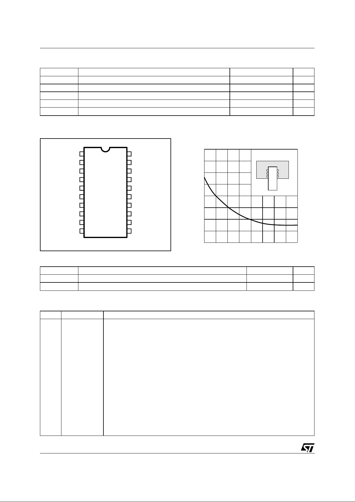
PIN CONNECTION (Top view)
Rth with "on board" Square Heatsink vs. copper area.
R
-V
CC
-V
CC
-V
CC
OUT
BOOTDIODE
BOOT
N.C.
FEEDCAP
FREQ
SGN-GND 10 IN11
1
2
3
4
5
6
7
8
9 STBY/MUTE
D96AU537B
20
19
18
17
16
15
14
13
12
-V
CC
-V
CC
-V
CC
-V
CC
+V
CC POW
VREG
+V
CC SIGN
N.C.
thj-a
(˚C/W)
60
50
40
30
COPPER AREA 35µ
THICKNESS
PC BOARD
D97AU675
0 4 8 12 Area(cm2)
THERMAL DATA
Symbol Parameter Value Unit
R
th j-amb
R
th j-pin
Thermal Resistance Junction to ambient 80 °C/W
Thermal Resistance Junction to Pin Max. 12 °C/W
PIN FUNCTIONS
N. Name Function
2/10
1
2
3
4
5
6
7
8
9
10
11
12
13
14
15
16
17
18
19
20
-V
CC
-V
CC
-V
CC
OUT
BOOTDIODE
BOOT
NC
FEEDCAP
FREQUENCY
SGN-GND
IN
ST-BY-MUTE
NC
+V
SIGN
CC
VREG
+V
POW
CC
-V
CC
-V
CC
-V
CC
-V
CC
NEGATIVE SUPPLY.
NEGATIVE SUPPLY.
NEGATIVE SUPPLY.
PWM OUTPUT
BOOTSTRAP DIODE ANODE
BOOTSTRAP CAPACITOR
NOT CONNECTED
FEEDBACK INTEGRATING CAPACITANCE
SETTING FREQUENCY RESISTOR
SIGNAL GROUND
INPUT
ST-BY/ MUTE CONTROL PIN
NOT CONNECTED
POSITIVE SIGNAL SUPPLY
10V INTERNAL REGULATOR
POSITIVE POWER SUPPLY
NEGATIVE SUPPLY (TO BE CONNECTED TO PIN 16 VIA C5)
NEGATIVE SUPPLY
NEGATIVE SUPPLY
NEGATIVE SUPPLY
TDA7480
ELECTRICAL CHARACTERISTICS (Refer to the test circuit, V
= 12KΩ; Demod.. filter L = 60µH, C = 470nF; f = 1KHz; T
R
f
= ±14V; RL = 8Ω; RS = 50Ω;
CC
= 25°C unless otherwise specified.)
amb
Symbol Parameter Test Condition Min. Typ. Max. Unit
V
S
I
q
V
OS
P
O
P
(*) Dissipated Power at 1W Output
d
Supply Range
Total Quiescent Current RL = ∞; NO LC Filter 25 40 mA
Output Offset Voltage Play Condition –50 +50 mV
Output Power THD = 10%
THD = 1%
R
= 4Ω VCC = ±10.5V
L
THD = 10%
THD = 1%
Rf = 12KΩ PΟ = 1W 1 W
±
8.5
10
6
10
10
16 V
±
W
7
W
W
7
W
Power
P
DMAX
η
THD Total Harmonic Distortion R
I
max
Maximum Dissipated Power PΟ = 10W THD 10%
R
= 38°C/W (Area 12cm2)
th-j-amb
P
Efficiency ≡
O
PO + P
D
Overcurrent Protection
≡
P
O
(**)
P
I
THD 10%
R
= 38°C/W (Area 12cm2)
th-j-amb
= 8Ω; PO = 0.5W 0.1 %
L
RL = 0 3.5 5 A
1.8 W
80 85 %
Threshold
T
j
Thermal Shut-down Junction
150 °C
Temperature
G
V
e
N
R
i
Closed Loop Gain 29 30 31 dB
Total Input Noise A Curve
f = 20Hz to 22KHz
12
7
µ
µ
Input Resistance 20 30 K
V
V
Ω
SVR Supply Voltage Rejection f = 100Hz; Vr = 0.5 46 60 dB
T
r
R
DSON
F
F
SW_OP
, T
SW
Rising and Falling Time 50 ns
f
Power Transistor on Resistance 0.4
Switching Frequency 100 120 140 KHz
Switching Frequency Operative
100 200 KHz
Ω
Range
B
F
Zero Signal Frequency
1.4x10
9
Hz
Ω
Constant (***)
R
F
Frequency Controller Resistor
71214K
Ω
Range (****)
MUTE & STAND-BY FUNCTIONS
V
ST-BY
V
MUTE
V
PLAY
A
MUTE
I
qST-BY
*: The output average power when the amplifier is playing music can be considered roughly 1/10 of the maximum output power. So it is useful
to consider the dissipated power in this condition for thermal dimensioning.
**: P
= measured across the load using the following inductor:
O
COIL 58120 MPPA2 (magnetics) TURNS: 28 ∅ 1mm
COIL77120 KOOL M
***: The zero-signal switching frequency can be obtained using the following expression: F
****: The maximum value of RF is related to the maximum possible value for the voltage drop on RF itself.
(1): For V
Stand-by range 0.8 V
Mute Range 1.8 2.5 V
Play Range (1) 4 V
Mute Attenuation 60 80 dB
Quiescent Current @ Stand-by 3 5 mA
(magnetics) TURNS: 28
µ
>5.2V, an input impedance of 10KΩ is to be considered.
12
∅
1mm
SW
= BF/R
F
3/10

TDA7480
Figure 2: Recomended P.C. Board and Component Layout of the Circuit of Figure1 (1.25:1 scale).
Note: Capacitor C5 must be as close as possible to device’s pins 16 and 17
4/10

Figure 3: Stereo Application in Single Supply.
(*) +5V
MUTE/
ST-BY
IN LEFT
MUTE/
ST-BY
IN RIGHT
(*) +5V Referred to VCC/2
R1 10K
R3
30K
2.2µF
C2 0.33µF
C4 4.7nF
C16 0.33µF
C18 4.7nF
R2
10K
MUTE ST-BYC1
SGN-GND
ST-BY/MUTE
C3
1nF
FEEDCAP
C8
270pF
SGN-GND
ST-BY/MUTE
C17
1nF
FEEDCAP
C24
270pF
N.C.
7,13
10
12
IN
11
8
9
C19 100nF
N.C.
7,13
10
12
IN
11
8
9
TDA7480
FREQ
R4
12KΩ
TDA7480
FREQ
R8
12KΩ
-VCC
(Pin 17)
V
CC
14,16
LEFT
1,2,3,17,
18,19,20
V
CC
14,16
RIGHT
1,2,3,17,
18,19,20
C5 100nF
-V
CC SIGN
100nF
-V
CC SIGN
C22
100nF
TDA7480
C29
2200µF/
50VI
C30
2200µF/
50VI
+VS
L2 1µH
D97AU815C
R6
1K/2W
R7
1K/2W
C14
470nF
C28
470nF
C7
47µF/50VI
C10
47µF/50VI
L3 1µH
L4 1µH
C21
47µF/50VI
C23
47µF/50VI
L7 1µH
L8 1µH
OUT R
PGND
OUT R
PGND
L6 1µH
OUT
LEFT
OUT
RIGHT
C6
100nF
6
BOOT
C11
100nF
4
OUT
5
BOOTDIODE
15
VREG
C9
C20
100nF
6
BOOT
C25
100nF
4
OUT
5
BOOTDIODE
15
VREG
C15
100nF
C27
100nF
C12
560pF
R5
150Ω
C26
560pF
R9
150Ω
L1 60µH
L5 60µH
5/10

TDA7480
Figure 4: PC Board and component Layout of the Circuit of Figure 3.
6/10

TYPICAL CHARACTERISTICS (Application Circuit of fig 1 unless otherwise specified)
TDA7480
Figure 5. Output Power vs. Supply Voltage
Output Power (W)
16
15
14
13
12
11
10
9
8
7
6
5
4
3
2
1
0
10 10.5 11 11.5 12 12.5 13 13.5 14 14.5 15 15.5 16
Rl= 8 Ohm
F= 1 KHz
Thd=10%
Thd=1%
Supply Voltage (+/- V)
Figure 7. Distortion vs. Output Power
THD (%)
10
1
Vs= +/- 10.5V
0.1
012345678910
Output Power (W)
Rl= 4 Ohm
F= 1 KHz
Figure 6. Distortion vs. Output Power
THD (%)
10
1
0.1
0.01
012345678910
Vs= +/- 14V
Rl= 8 Ohm
F= 1 KHz
Output Power (W)
Figure 8. Power Dissipation and Efficiency vs.
Output Power
Power Dissipation (W)
2
1.8
1.6
1.4
1.2
1
0.8
0.6
0.4
0.2
0
012345678910
Efficiency
Pdiss
Output Power (W)
Efficiency (%)
Vs= +/- 14V
Rl= 8 Ohm
F= 1 KHz
100
80
60
40
20
0
Figure 9. Power Dissipation and Efficiency vs.
Output Power
Power Dissipation (W)
2.5
Efficiency
2
1.5
1
Pdiss
0.5
0
012345678910
Output Power (W)
Vs= +/- 10.5V
Rl= 4 Ohm
F= 1 KHz
Efficiency (%)
100
90
80
70
60
50
40
30
20
10
0
Figure 10. Mute Attenuation vs. Vpin 12
Attenuation (dB)
20
10
0
Vs= +/- 14V
Rl= 8 Ohm
-10
0 dB =1 W @ F= 1 KHz
-20
-30
-40
-50
-60
-70
-80
-90
-100
-110
-120
0 0.5 1 1.5 2 2.5 3 3.5 4 4.5 5
Vpin #12 (V)
7/10

0
TDA7480
Figure 11. Supply Voltage Rejection vs. Fre-
quency
S.V.R. (dB)
0
-10
-20
-30
-40
-50
-60
-70
-80
-90
-100
-110
-120
0.01 0.1 1 1
Vs= +/- 14V
Rl= 8 Ohm
Rs= 50 Ohm
Vr=0.5Vrms
Frequency (KHz)
8/10

POWERDIP20 PACKAGE MECHA NICAL DATA
TDA7480
DIM.
MIN. TYP. MAX. MIN. TYP. MAX.
a1 0.51 0.020
B 0.85 1.40 0.033 0.055
b 0.50 0.020
b1 0.38 0.50 0.015 0.020
D 24.80 0.976
E 8.80 0.346
e 2.54 0.100
e3 22.86 0.900
F 7.10 0.280
I 5.10 0.201
L 3.30 0.130
Z 1.27 0.050
mm inch
9/10

TDA7480
Information furnishe d is beli eved to be accu rate and reliable. However, STMicroelec tronics assumes no res ponsibility for the consequences
of use of such i nformation nor for any i nfringement of patents or ot her rights of third par ties which may result from its use. No license i s
granted by impli cation or otherwis e under any patent or patent righ ts of STMicroelect ronics. Specifica tion mentioned in this publication are
subject to change without notic e. This public ation supers edes and replaces all information prev iously supplied. STMic roelec tronic s products
are not authorized for use as critical components in life support devices or systems without express written approval of STMicroelectronics.
The ST logo is a registered trademark of STMicroelect roni cs
© 1998 STMicroelectronics – Printed in Italy – All Rights Reserved
STMicroelectronics GROUP OF COMPANIES
Australia - Brazil - Canada - China - France - Germany - Italy - Japan - Korea - Malaysia - Malta - Mexico - Morocco - The Netherlands -
Singapore - Spain - Sweden - Switzerland - Taiwan - Thailand - United Kingdom - U.S.A.
http://w ww.s t.com
10/10
 Loading...