

DIGITALLYCONTROLLEDAUDIO PROCESSOR WITH
SRS SURROUND SOUND AND VOICE CANCELLER
The Device incorporates the SRS
(Sound Retrieval System) under
licencefromSRS Labs, Inc.
1 STEREOINPUT
INPUT ATTENUATION CONTROL IN 0.5dB
STEP
TREBLEMIDDLE ANDBASS CONTROL
VOICECANCELLERIS AVAILABLE
STEREO SRS SURROUND SOUND WITH
CENTER& SPACECONTROL IS AVAILABLE
THREE STANDARD SURROUND MODES
ARE AVAILABLE:
- MUSICIN 4 DIFFERENTSELECTABLE
RESPONSES
- MOVIE ANDSIMULATED IN256
DIFFERENTSELECTABLE RESPONSES
2 SPEAKERSOUTPUTS
- INDEPENDENTATTENUATORS IN1dB
STEPFOR BALANCEFACILITY
- ZEROCROSSINGATTENUAT IONAVAILABLE
- AVAILABILITYOF LOUDSPEAKERS
EQUALIZATION FIXEDBY EXTERNAL
COMPONENTS
- INDEPENDENTMUTE FUNCTION
2 RECORD OUTPUTS
- INDEPENDENTATTENUATORS IN1dB
STEPFOR BALANCEFACILITY
- MUXAVAILABLE FORPROCESSESSIGNAL
SELECTIO N
- INDEPENDENTMUTE FUNCTION
ALL FUNCTIONS PROGRAMMABLE VIA SERIAL BUS
DESCRIPTION
The TDA7466 is a volume tone (bassmiddle and
treble) balance (Left/Right) processorswith stereo
SRS and voicecanceller for quality audio applications in car radio, Hi-Fi, TV systems.
It reproduces SRS (Sound Retrieval System)
sound by external components and surround
sound by using phase shifters and a signal matrix. The AC signal setting is obtained by resistor
networks and switches combined with operational
amplifiers according to the SRS laboratories
specification. Control of all the functions is ac-
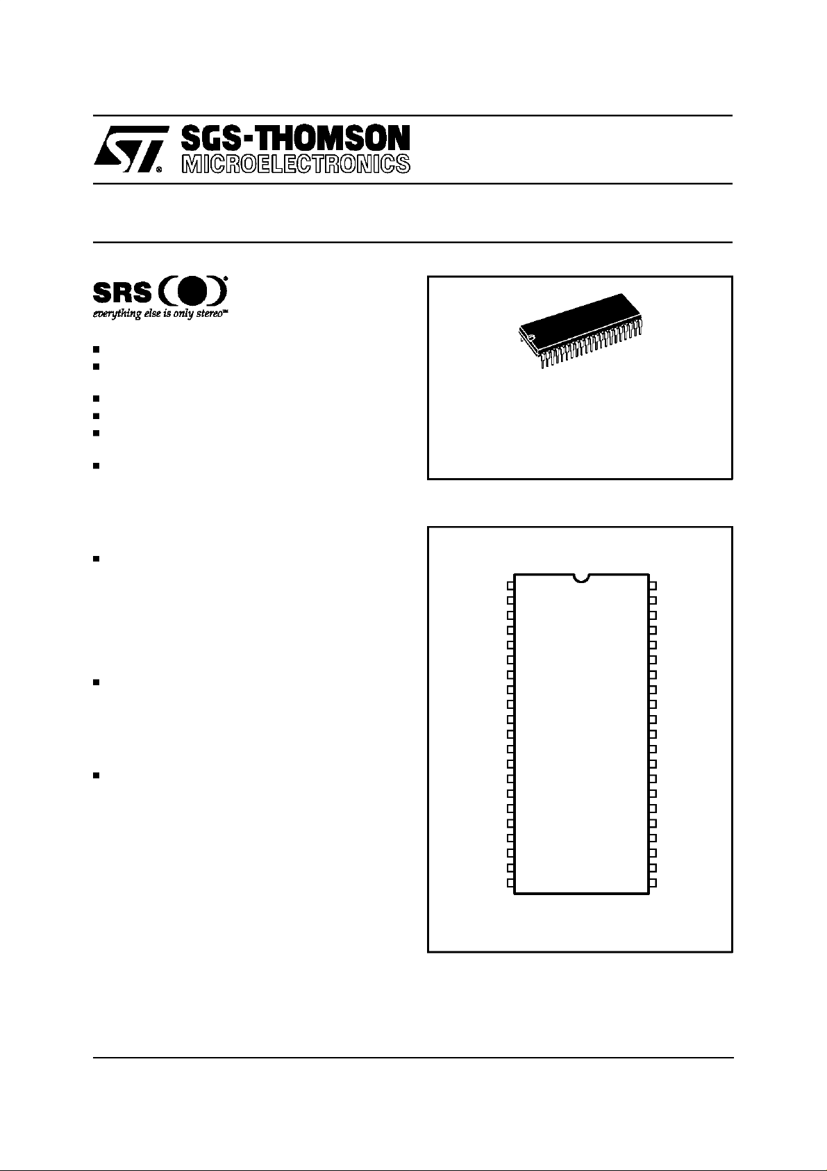
TDA7466
SDIP42
ORDERING NUMBER: TDA7466
PIN CONNECTION
1
V
S
LP
LP1
2
3
4
5
6
7
8
9
10
11
12
13
14
15
16
17
18
19
20
21
D96AU445A
PS4
PS3
PS2
PS1 R_IN
HP1
HP2
VAR_L
BASSO_L
VAR_R
BASSO_R
BASS_LO
BASS_LI
BASS_RO
BASS_RI
MIDDLE_LO
MIDDLE_LI
MIDDLE_RO
MIDDLE_RI
complishedby serialbus.
Thanks to the used BIPOLAR/CMOSTechnology,
Low Distortion, Low Noise and DC stepping are
obtained.
42
41
40
39
38
37
36
35
34
33
32
31
30
29
27
26
25
24
23
22
CREF
NBRO
NBRIN
LPVC
VREFOUT
L_IN
NBLIN
NBLO
NETW2
NETW1
RECOUT_L
RECOUT_R
L_OUT
R_OUT28
DIG_GND
SCL
SDA
AGND
TREBLE_L
TREBLE_R
May 1997
1/21
TDA7466
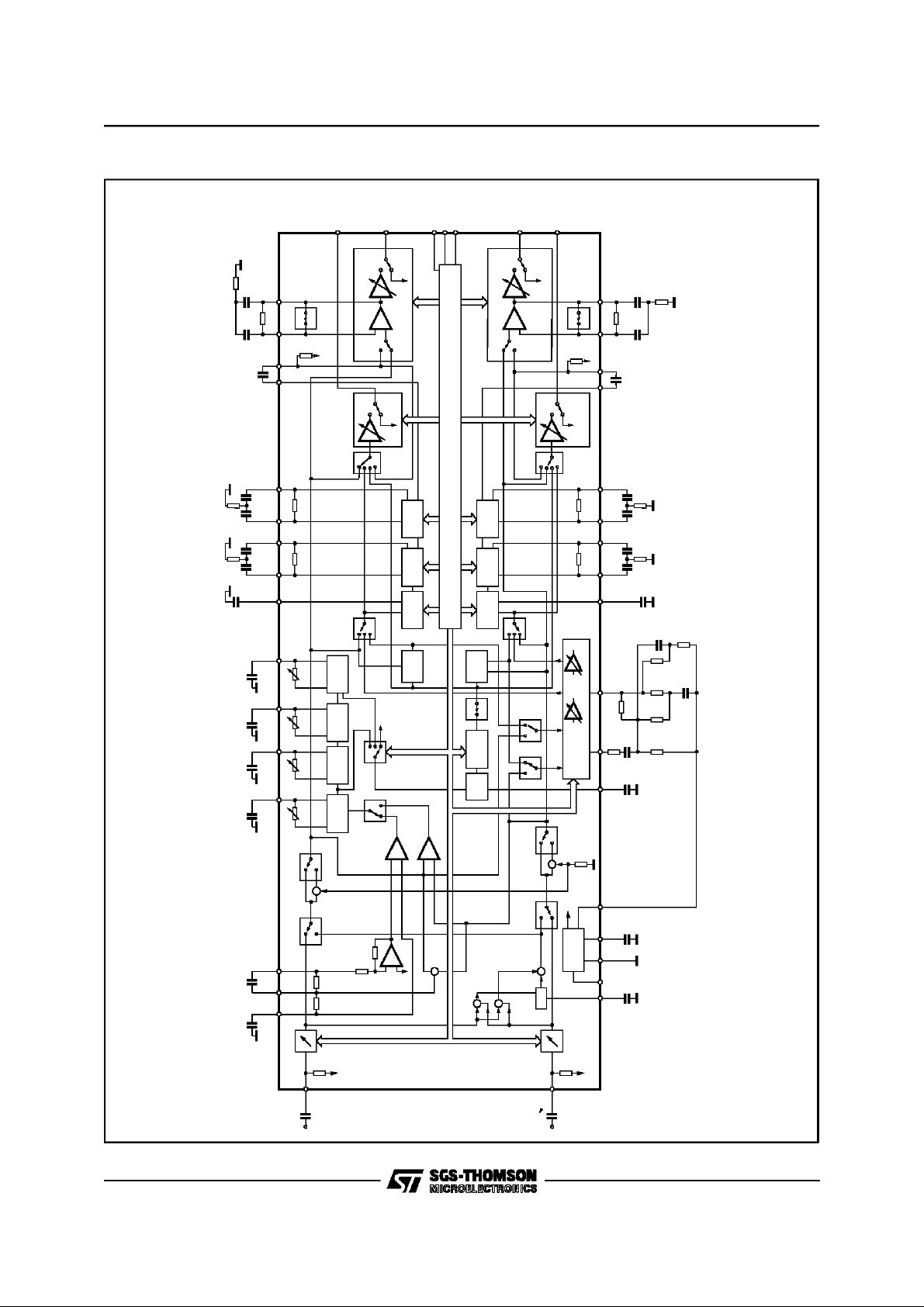
BLOCK DIAGRAM
SCL
SDA
DIG_GND
262527
79dB CONTROL
ATT
REC
79dB CONTROL
SPKR
-
VAR
L-OUT
29
ATT
MUTE
+
FIX
MUTE
RECOUT-L
31
NB1
3435
NB2
NBLIN NBLO
NB-LA NB-LB
2.2µF
30K
BASSO-L VAR-L
ATT
SPKR
79dB CONTROL
+
FIX
28
R-OUT
-
VAR
MUTE
REC
RECOUT-R
30
ATT
MUTE
D96AU446B
NB4
NB3
NBRIN NBRO
30K
1213162239
BASSO-R VAR-R
79dB CONTROL
NB-RA NB-RB
2.2µF
5.6K
2.7K
100nF
100nF
22nF
18nF
5.6nF
22nF
22nF
4.7nF
100nF
5.6nF 680nF
BASS-LO
14 11 10
BASS-LI
MIDDLE-LO
MIDDLE-LI
19 18 15
23
TREBLE-L
PS4
PS3
PS2
PS1
789 5 4 3 2
LP1 HP1 HP2
31.5dB control
SRS
SIM
MOVIE/
R6
REAR
SURR
OFF
-
3BAND
C BUS DECODER + LATCHES
2
I
BASS
MIDDLE
TREBLE
AMP
MIXING
MUSIC
SIM
MOVIE/
-
L-R
-
+
+
+
+
FIX
RB
RM
RPS4
RPS3
RPS2
RPS1
MIX SW
36
L-IN
0.22µF
SURR
FIX
PS4
400Hz
PS3
400Hz
MUSIC
PS2
4KHz
PS1
90Hz
+
R5
RHP1
RLP1
50K
AMP
MIXING
EFFECT
CONTROL
LPF
9KHz
+
TREBLE MIDDLE BASS
FIX
-
SURR
3BAND
FIX
SRS
VOICE
BASS-RO
SURR
REAR
RM RB
21 20 17
CENTER SPACE
SRS
32 33
STEREO
100K
+
REF
V
37 40 41
ON
SUPPLY
+LPF
12442 6
31.5dB
control
50K
38
R-IN
100K
0.22µF
NETW2NETW1
1K
LP
CREF
AGND
S
V
LPVC TREBLE-R
BASS-RI
100nF 100nF
MIDDLE-RO
18nF 22nF
MIDDLE-RI
130K
0.47µF
1.2nF
VREFOUT
22µF
100nF
5.6nF
5.6K
2.7K
4.7nF
3.74K
47.5K
0.47µF
1.5K 32.4K
4.42K
2/21
TDA7466
THERMAL DATA
Symbol Description Value Unit
R
thj-pins
ABSOLUTE MAXIMUM RATINGS
Symbol Parameter Value Unit
V
T
amb
T
QUICK REFERENCE DATA
Symbol Parameter Min. Typ. Max. Unit
V
V
THD Total Harmonic Distortion V = 1Vrms f= 1KHz 0.01 0.1 %
S/N Signal to Noise Ratio V
S
Thermal Resistance Junction-pins Max. 85 °C/W
Operating Supply Voltage 11 V
S
Operating Ambient Temperature -10 to 85
Storage Temperature Range -55 to +150 °C
stg
Supply Voltage 7 9 10.2 V
S
CL
Max. input signal handling 2 Vrms
out = 1Vrms (mode = OFF) 106 dB
Channel Separation f = 1KHz 90 dB
C
Input Attenuation Control (0.5dB) -31.5 0 dB
Treble Control (2db step) -14 +14 dB
Middle Control (2db step) -14 +14 dB
Bass Control (2dB step) -14 +14 dB
Balance Control 1dB step (L
CH, RCH) -79 0 dB
Mute Attenuation 100 dB
C
°
ELECTRICALCHARACTERISTICS (refer to the test circuit T
= 1Vrms;RG= 600Ω, allcontrols flat (G = 0dB),Effect Ctrl = -6dB, MODE= OFF; f = 1KHz
V
in
=25°C, VS= 9V,RL= 10KΩ,
amb
unless otherwise specified)
Symbol Parameter Test Condition Min. Typ. Max. Unit
SUPPLY
V
S
I
S
SVR Ripple Rejection L
Supply Voltage 7 9 10.2 V
Supply Current 25 mA
CH /RCH out, Mode = OFF 60 80 dB
INPUTSTAGE
R
IN
V
CL
A
RANGE
A
VMIN
A
VMAX
A
STEP
V
DC
A
VO1
A
VO2
Input Resistance 37.5 50 62.5 KΩ
Clipping Level THD = 0.3% 2 2.5 Vrms
Attenuation Range 31.5 dB
Min. Attenuation -1 0 1 dB
Max. Attenuation 31 31.5 32 dB
Step Resolution -1 0.5 1 dB
DC Steps Adjacent att. step -3 0 3 mV
Voice Canceller Output 1 LIN=RIN,RIN=ON,
V
= 0V FIX, 0dB attenuation
mix
Voice Canceller Output 2 LIN=RIN=0VV
mix
=1V
rms
FIX,
567dB
-1 0 1 dB
0dB attenuation
3/21
TDA7466
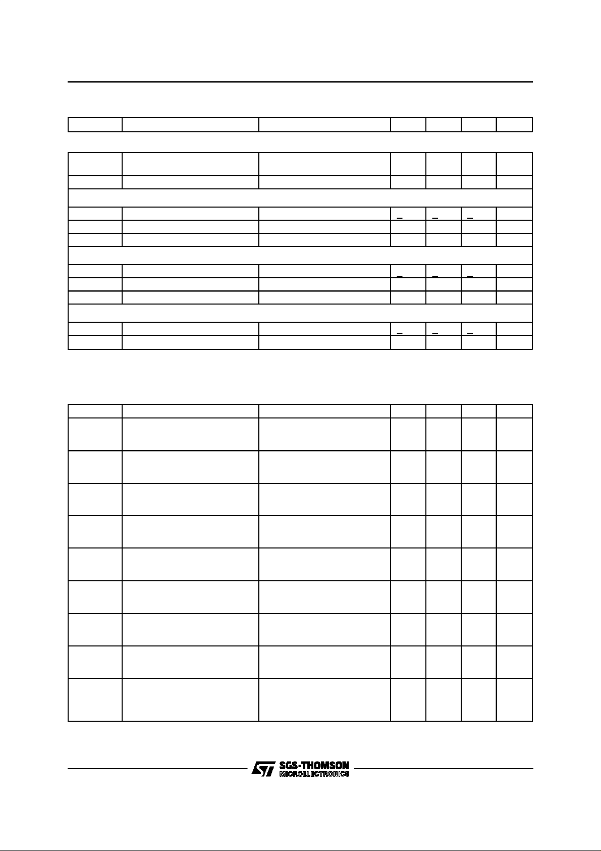
ELECTRICALCHARACTERISTICS (continued)
Symbol Parameter Test Condition Min. Typ. Max. Unit
SUPPLY
A
VO3
Voice Canceller Output 3 LIN=-RIN,V
= 0V FIX,
mix
567dB
0dB attenuation
R
LPV
Low Pass Filter Resistance 24 32 40 KΩ
BASSCONTROL
Gb Control Range Max. Boost/cut +12.0 +14.0 +16.0 dB
B
STEP
R
B
Step Resolution 1 2 3 dB
Internal Feedback Resistance 33 44 55 KΩ
MIDDLE CONTROL
Gm Control Range Max. Boost/cut +12.0 +14.0 +16.0 dB
M
STEP
R
M
Step Resolution 1 2 3 dB
Internal Feedback Resistance 18.75 25 31.25 K
TREBLECONTROL
Gt Control Range Max. Boost/cut +13.0 +14.0 +15.0 dB
T
STEP
Step Resolution 1 2 3 dB
STANDARDSURROUND SOUND MATRIX
TEST CONDITION (PhaseResistor Selection D0=0, D1=1, D2=0. D3=1, D4=0,D5=1, D6=0,D7=1
Symbol Parameter Test Condition Min. Typ. Max. Unit
G
D
OFF
GOFF
In-phase Gain (OFF) Mode OFF, Input signal of
LR In-phase Gain Difference
(OFF)
G
MOV
D
GMOV
In-phase Gain (Movie) Movie mode, Effect Ctrl = -6dB
LR In-phase Gain Difference
(Movie)
G
MUS
D
GMUS
In-phase Gain (Music) Music mode, Effect Ctrl = -6dB
LR In-phase Gain Difference
(Music)
L
MON1
L
MON2
L
MON3
Simulated L Output 1 SimulatedMode,EffectCtrl= -6dB
Simulated L Output 2 SimulatedMode,EffectCtrl= -6dB
Simulated L Output 3 SimulatedMode, EffectCtrl= -
1kHz, 1.4 V
Lin→ L
out
p-p,Rin
→
R
out
Mode OFF, Input signal of
1kHz, 1.4 V
R
→
in
Input signal of 1kHz, 1.4 V
R
→
in
R
out,Lin
R
out,Lin
p-p
→
→
L
out
L
p-p
out
Movie mode, Effect Ctrl = -6dB
Input signal of 1kHz, 1.4 V
(Rin→ R
)–(Lin→ L
out
Input signal of 1kHz, 1.4 V
(Rin→ R
), (Lin→ L
out
out
out
p-p
)
p-p
)
Music mode, Effect Ctrl = -6dB
Input signal of 1kHz, 1.4 V
(Rin→ R
)-(Lin→ L
out
out
p-p
)
Input signal of 250Hz,
1.4 V
p-p,Rin
and L
L
→
in
out
Input signal of 1kHz,
1.4 V
p-p,Rin
and Lin→ L
out
6dB
Input signal of 3.6kHz,
1.4 V
p-p,Rin
and Lin→ L
out
-1 0 1 dB
-1 0 1 dB
8dB
0dB
7dB
0dB
4.5 dB
– 4.0 dB
7.0 dB
Ω
4/21

TDA7466
ELECTRICALCHARACTERISTICS (continued)
Symbol Parameter Test Condition Min. Typ. Max. Unit
R
MON1
R
MON2
R
MON3
R
LP1
R
HPI
R
LPF
STANDARDSURROUND SOUND EFFECT CONTROL
C
RANGE
S
STEP
SURROUND SOUNDMATRIX PHASE
R
PS10
R
PS11
R
PS12
R
PS13
R
PS20
R
PS21
R
PS22
R
PS23
R
PS30
R
PS31
R
PS32
R
PS33
R
PS40
R
PS41
R
PS42
R
PS43
Simulated R Output 1 SimulatedMode,EffectCtrl= -6dB
– 4.5 dB
Input signal of 250Hz,
1.4 V
Simulated R Output 2 SimulatedMode,EffectCtrl= -6dB
p-p,Rin
and Lin→R
out
3.8 dB
Input signal of 1kHz,
1.4 V
p-p,Rin
and L
Simulated R Output 3 SimulatedMode,EffectCtrl= -6dB
R
→
in
out
–20 dB
Input signal of 3.6kHz,
1.4 V
p-p,Rin
and L
R
→
in
out
Low Pass Filter Resistance 7.5 10 12.5 KΩ
High Pass Filter Resistance 45 60 75 K
LP Pin Impedance 7.5 10 12.5 KΩ
Control Range - 21 - 6 dB
Step Resolution 1 dB
Phase Shifter 1:D1 = 0, D0 = 0 8.8 11.8 14.8 KΩ
Phase Shifter 1:D1 = 0, D0 = 1 10.6 14.1 17.6 K
Phase Shifter 1:D1 = 1, D0 = 0 13.4 17.9 22.4 KΩ
Phase Shifter 1:D1 = 1, D0 = 1 28 37.3 46.6 KΩ
Phase Shifter 2:D3 = 0, D2 = 0 4.2 5.6 7 K
Phase Shifter 2:D3 = 0, D2 = 1 5.1 6.8 8.5 KΩ
Phase Shifter 2:D3 = 1, D2 = 0 6.3 8.4 10.5 K
Phase Shifter 2:D3 = 1, D2 = 1 13.7 18.3 22.9 KΩ
Phase Shifter 3:D5 = 0, D4 = 0 9 12.1 15.1 K
Phase Shifter 3:D5 = 0, D4 = 1 10.9 14.5 18.1 KΩ
Phase Shifter 3:D5 = 1, D4 = 0 13.6 18.1 22.6 KΩ
Phase Shifter 3:D5 = 1, D4 = 1 29.3 39.1 48.9 KΩ
Phase Shifter 4:D7 = 0, D6 = 0 9 12.1 15.1 KΩ
Phase Shifter 4:D7 = 0, D6 = 1 10.9 14.5 18.1 K
Phase Shifter 4:D7 = 1, D6 = 0 13.6 18.1 22.6 KΩ
Phase Shifter 4:D7 = 1, D6 = 1 29.3 39.1 48.9 K
Ω
Ω
Ω
Ω
Ω
Ω
Ω
SRS SURROUND SOUND MATRIX
CENTER SRS Control Range -31 0 dB
Step
SPACE SRS Space Control Range -31 0 dB
Step
P
ERSP1
P
ERSP2
L+R L+ R SRS Curve SPACE= MUTE,CENTER
Center Step Resolution 1 dB
C
Space Step Resolution 1 dB
S
Perspective 1 Input Signal of 125Hz
12 dB
SPACE= 0dB,CENTER= MUTE
R
in = GND; Lin → ROUT
Perspective 2 Input Signal of 2.15KHz
0dB
SPACE= 0dB,CENTER= MUTE
R
= GND; Lin→ R
in
OUT
-8.5 dB
=0dB
R
= GND; Li
in
n →ROUT
5/21
TDA7466
ELECTRICALCHARACTERISTICS (continued)
Symbol Parameter Test Condition Min. Typ. Max. Unit
SPEAKER & RECORDATTENUATORS
C
range
S
STEP
E
A
V
DC
A
MUTE
R
VAR
SPEAKER ATTENUATORS
V
TH
AUDIOOUTPUTS
N
O(OFF)
N
O(MOV)
N
O(MUS)
N
O(SIM)
N
O(SRS)
d Distorsion Av = 0 ; V
S
C
V
OCL
R
OUT
V
OUT
BUS INPUTS
V
IL
V
IH
I
IN
V
O
Control Range 79 dB
Step Resolution 0.5 1 1.5 dB
Attenuation set error Av = 0 to -20dB -1.5 0 1.5 dB
Av = -20 to -79dB -3 0 2 dB
DC Steps Adjacent att. steps -3 0 3 mV
Output Mute Condition 70 100 dB
Input Impedance 22.5 30 37.5 KΩ
Zero CrossingThreshold D7 = 0
Output Noise (OFF) Output Mute, Flat
B
= 20Hz to 20KHz
W
Output Noise (Movie) Standard
Surround Sound
Output Noise (Music) Standard
Surround Sound
Output Noise (Simulated)
Standard Surround Sound
Output Noise (SRS)
Mode =Movie ,
B
= 20Hz to 20KHz
W
Mode = Music ,
B
= 20Hz to 20KHz,
W
Mode = Simulated,
B
= 20Hz to 20KHz
W
BW= 20Hz to 20KHz 50
V
S
+
20
2
4
5
30 µVrms
30
30 µVrms
Surround Sound
= 1Vrms 0.01 0.1 %
in
Channel Separation 70 90 dB
Clipping Level d = 0.3% 2 2.5 Vrms
Output Resistance 10 30 50
DC Voltage Level 3.8 V
Input Low Voltage 1V
Input High Voltage 3 V
Input Current -5 +5 µA
Output Voltage SDA
IO= 1.6mA 0.4 V
Acknowledge
mV
Vrms
µ
µVrms
Vrms
µ
Vrms
µ
Ω
6/21
TDA7466
I2C BUSINTERFACE
Data transmission from microprocessor to the
TDA7466 and viceversa takes place through the
2 wires I
2
C BUS interface, consisting of the two
lines SDA and SCL (pull-up resistors to positive
supply voltage mustbe connected).
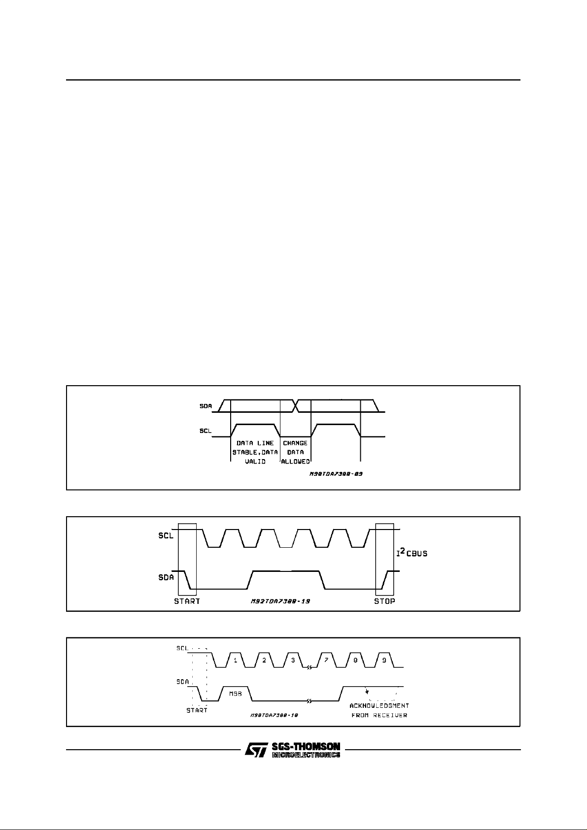
Data Validity
As shown in fig. 3, the data on the SDA line must
be stable during the high period of theclock. The
HIGH and LOW state of the data line can only
change when the clock signal on the SCL line is
LOW.
Start andStop Conditions
As shown in fig.4 a start condition is a HIGH to
LOW transition of the SDA line while SCL is
HIGH. The stop condition is a LOWto HIGH transition of the SDA linewhile SCL is HIGH.
Byte Format
Every byte transferred on the SDA line must con-
tain 8 bits. Each byte must be followed by an ac-
2
Figure 3: Data Validity on theI
CBUS
knowledgebit. The MSB is transferredfirst.
Acknowledge
The master (µP) puts a resistiveHIGHlevelon the
SDA line during the acknowledge clock pulse(see
fig. 5). The peripheral (audioprocessor) that acknowledges has to pull-down (LOW) the SDA line
duringthisclock pulse.
The audioprocessor which has been addressed
has to generate an acknowledge after the reception of each byte, otherwise the SDA line remains
at the HIGH level during the ninth clock pulse
time. In this case the master transmitter can generate the STOP information in order to abort the
transfer.
Transmission without Acknowledge
Avoiding to detect the acknowledge of the audio-
processor,the µP can use a simpler transmission:
simply it waits one clock without checking the
slaveacknowledging,and sends the new data.
This approach of course is less protected from
misworking.
Figure 4: TimingDiagram of I
2
Figure 5: Acknowledgeon the I
CBUS
2
CBUS
7/21

TDA7466
SOFTWARESPECIFICATION
InterfaceProtocol
The interfaceprotocol comprises:
A start condition (S)
address
A subaddressbytes
A sequenceof data (N byte + achnowledge)
A stopcondition (P)
A chip address byte, containing the TDA7466
CHIP ADDRESS
MSB LSB MSB LSB MSB LSB
S100000A0ACK ACK DATA ACK P
D95AU226A
SUBADDRESS DATA 1 to DATA n
B DATA
ACK = Achnowledge
S = Start
P = Stop
A = Address
B = AutoIncrement
EXAMPLES
No IncrementalBus
rect chip address, a subaddresswith the MSB= 0
(no incremental bus), N-data (all these data concern the subaddressselected), a stop condition.
The TDA7466 receives a start condition, the cor-
CHIP ADDRESS
MSB LSB MSB LSB MSB LSB
S100000A0ACK ACK DATA ACK P
D95AU306
Incremental Bus
The TDA7466 receives a start condition, the correct chip address,a subaddresswith the MSB = 1
(incremental bus): now it is in a loop condition
with an autoincrease of the subaddress whereas
CHIP ADDRESS
MSB LSB MSB LSB MSB LSB
S100000A0ACK ACK DATA ACK P
D95AU307
SUBADDRESS DATA
0D3
X X X D2 D1 D0
SUBADDRESS from ”1XXX1010” to ”1XXX1111”
of DATAare ignored.
The DATA 1 concerns thesubaddress sent, and
the DATA 2 concerns the subaddress sent plus
one in the loop etc. and, at the end, it receives the
stop condition.
SUBADDRESS DATA 1 to DATA n
1D3
X X X D2 D1 D0
8/21

DATA BYTES (Address= 80(HEX)):
FUNCTIONSELECTION:
The firstbyte (subaddress)
MSB LSB SUBADDRESS
D7 D6 D5 D4 D3 D2 D1 D0
BXXX0000INPUT ATTENUATION
BXXX0001SURROUND & OUT & EFFECT
CONTROL
BXXX0010PHASERESISTOR
BXXX0011BASS& NATURAL BASE
BXXX0100MIDDLE & TREBLE
BXXX0101SPEAKERATTENUATION ”L”
BXXX0110SPEAKERATTENUATION ”R”
BXXX0111RECORD ATTENUATION ”L”
BXXX1000RECORD ATTENUATION”R”
BXXX1001INPUT MULTIPLEXER, VOICE
CANCELLER & REC OUT
BXXX1010SRS/SPACE ATTENUATION
BXXX1011SRS/CENTER ATTENUATION
B = 1 INCREMENTAL BUS; ACTIVE
B = 0 NOINCREMENTAL BUS;
X = DONT’CARE
TDA7466
INPUT ATTENUATION SELECTION
MSB LSB INPUT ATTENUATION
D7 D6 D5 D4 D3 D2 D1 D0 0.5 dB STEPS
1 000 0
1 0 0 1 -0.5
1 010 -1
1 0 1 1 -1.5
1 100 -2
1 1 0 1 -2.5
1 110 -3
1 1 1 1 -3.5
4 dB STEPS
1000 0
1001 -4
1010 -8
1011 -12
1100 -16
1101 -20
1110 -24
1111 -28
INPUT ATTENUATION= 0 ∼ -31.5dB
9/21

TDA7466
STANDARD SURROUND SELECTION
MSB LSB
D7 D6 D5 D4 D3 D2 D1 D0 SURROUND MODE
0 0 SIMULATED
0 1 MUSIC
1 0 OFF
1 1 MOVIE
OUT
0 VAR
1 FIX
EFFECT CONTROL
0000 -6
0001 -7
0010 -8
0011 -9
0100 -10
0101 -11
0110 -12
0111 -13
1000 -14
1001 -15
1010 -16
1011 -17
1100 -18
1101 -19
1110 -20
1111 -21
PHASE RESISTORSELECTION
MSB LSB
D7 D6 D5 D4 D3 D2 D1 D0 PHASE SHIFT 1 (KΩ)
00 12
01 14
10 18
11 37
00 6
01 7
10 8
11 18
00 12
01 14
10 18
11 39
00 12
01 14
10 18
11 39
SURROUND PHASE
RESISTOR
PHASE SHIFT 2 (KΩ)
PHASE SHIFT 3 (KΩ)
PHASE SHIFT 4 (KΩ)
10/21

BASS SELECTION
MSB LSB BASS
D7 D6 D5 D4 D3 D2 D1 D0 2 dB STEPS
0000 -14
0001 -12
0010 -10
0011 -8
0100 -6
0101 -4
0110 -2
0111 0
1111 0
1110 2
1101 4
1100 6
1011 8
1010 10
1001 12
1000 14
NATURAL BASE
0
1
NBRIN, NBRO, NBLIN,
NBLO PIN ACTIVE
NO NBRIN, NBRO, NBLIN,
NBLO PIN
When external componentsaren’t connected, the data from NATURAL BASE must put ”OFF”
TDA7466
11/21

TDA7466
MIDDLE& TREBLESELECTION
MSB LSB MIDDLE
D7 D6 D5 D4 D3 D2 D1 D0 2 dB STEPS
0000 -14
0001 -12
0010 -10
0011 -8
0100 -6
0101 -4
0110 -2
0111 0
1111 0
1110 2
1101 4
1100 6
1011 8
1010 10
1001 12
1000 14
TREBLE
2 dB STEPS
0000 -14
0001 -12
0010 -10
0011 -8
0100 -6
0101 -4
0110 -2
0111 0
1111 0
1110 2
1101 4
1100 6
1011 8
1010 10
1001 12
1000 14
12/21

TDA7466
LEFT CHANNEL SPEAKER ATTENUATION SELECTION
MSB LSB SPEAKER/RECORD ATT
D7 D6 D5 D4 D3 D2 D1 D0 1 dB STEPS
000 0
001 -1
010 -2
011 -3
100 -4
101 -5
110 -6
111 -7
8 dB STEPS
0000 0
0001 -8
0010 -16
0011 -24
0100 -32
0101 -40
0110 -48
0111 -56
1000 -64
1001 -72
MUTE
101X
11XX
LEFT & RIGHTCHANNELS BOTH
MSB LSB ZERO CROSS ATT. MODE
D7 D6 D5 D4 D3 D2 D1 D0 1 dB STEPS
0 ON
1 OFF
X = DON’TCARE
SPEAKER/RECORDATTENUATION= 0dB
∼
-79dB
13/21

TDA7466
RECORDAND RIGHT CHANNEL SPEAKER ATTENUATION SELECTION
MSB LSB SPEAKER/RECORD ATT
D7 D6 D5 D4 D3 D2 D1 D0 1 dB STEPS
000 0
001 -1
010 -2
011 -3
100 -4
101 -5
110 -6
111 -7
8 dB STEPS
0000 0
0001 -8
0010 -16
0011 -24
0100 -32
0101 -40
0110 -48
0111 -56
1000 -64
1001 -72
MUTE
101X
11XX
X = DON’TCARE
SPEAKER/RECORDATTENUATION= 0dB
∼
-79dB
VOICE CANCELLER/INPUT/RECOUT L & R SELECTION
MSB LSB
D7 D6 D5 D4 D3 D2 D1 D0 VOICE CANCELLER
1 110 OFF
1 111 ON
REC OUT ”L”
1 0 0 1 1 VAR 1 (3BAND)
1 0 1 1 1 VAR 2 (SURR)
1 1 0 1 1 VAR 3 (REAR)
1 1 1 1 1 FIX
REC OUT ”R”
1 0 0 1 1 VAR 1(3BAND)
1 0 1 1 1 VAR 2 (SURR)
1 1 0 1 1 VAR 3 (REAR)
111 11 FIX
14/21

TDA7466
SRS SPACE CONTROL: ATTENUATION SELECTION
MSB LSB SPACE ATTENUATION
D7 D6 D5 D4 D3 D2 D1 D0 1 dB STEPS
000 0
001 -1
010 -2
011 -3
100 -4
101 -5
110 -6
111 -7
8 dB STEPS
000 0
001 -8
010 -16
011 -24
MUTE
1XXXXX
X = DON’TCARE
∼
SPEAKER/RECORDATTENUATION= 0dB
-31dB
SRS CENTER CONTROL:ATTENUATION SELECTION
MSB LSB CENTER ATTENUATION
D7 D6 D5 D4 D3 D2 D1 D0 1 dB STEPS
000 0
001 -1
010 -2
011 -3
100 -4
101 -5
110 -6
111 -7
8 dB STEPS
000 0
001 -8
010 -16
011 -24
MUTE
1XXXXX
SRS INPUT
0 NO SURROUND SIGNAL
1 SURROUND SIGNAL
SRS SWITCH
0 SRS ON
1 SRS OFF
X = DON’TCARE
∼
SPACEATTENUATION= 0dB
-31dB
RECOMMENDED TO ATTENUATE -3dB IN INPUTATTENUATION DURING ”SRS OFF”
TO FULFILL SRS BYPASSMODE WHEN SRS FUNCTION IS USED
15/21

TDA7466
POWER ON RESET
SURROUND & OUT CONTROL+ EFFECT CONTROL OFF + FIX + MAX ATTENUATION
SPEAKER/RECORD ATTENUATION L &R MODE MUTE + ZERO CROSS ATT.OFF
INPUT ATTENUATION + REAR SWITCH MAX ATTENUATION + ON
NATURAL BASE OFF
VOICE CANCELLER OFF
INPUT IN1
MIX SWITCH NO MIX PIN
SRS SURROUND OFF + MAX ATTENUATION
BASS & MIDDLE 2dB
TREBLE 0dB
PIN DESCRIPTION
PIN: L-OUT, R-OUT, RECOUT-L, RECOUT-R
V
S
10Ω
20µAGND
D96AU477
GND
GND
PIN: HP2
V
S
PIN: HP1
LP1
HP2
PIN: L-IN, R-IN
V
V
S
10K
60K
GND
D94AU198
S
16/21
HP1
GND
5.5K
60K
D94AU199
5.5K
20µA
GND
20µA
50K
V
REF
D94AU200

TDA7466
PIN: VAR-L, VAR-R,
V
S
SW
30K
Vref
GND
PIN: LP1
V
S
20µA
D95AU227
20µA
PIN: CREF
V
S
PIN: SCL, SDA
GND
20K
20K
20µA
42K
D95AU336
20µA
10K
GND
HP1
PIN: PS1, PS2, PS3, PS4, LP
V
S
GND
20µA
D94AU211
D95AU308
PIN: NETW2
GND
GND
D94AU205
V
S
20µA
D96AU473
17/21

TDA7466
PIN: BASSO-L,BASSO-R,NETW1
V
S
20µA
GND
D95AU230
PIN: BASS-LO,BASS-RO,MIDDLE-LO,MIDDLE-RO,
V
S
20µA
PIN: BASS-LI,BASS-RI,MIDDLE-LI,MIDDLE-R I,
V
S
20µA
45K
:
GND
BASS-LO
BASS-RO,MIDDLE-LO,MIDDLE-RO
or
25K
Bass
: MIDDLE
D95AU231A
PIN: TREBLE-L,TREBLE-R
V
S
20µA
(*)
GND
BASS-LI,BASS-RI,MIDDLE-LI,MIDDLE-RI
(*) 45K :
Bass
25K : MIDDLE
PIN: VOUT REF
V
S
20µA
GND
10K
GND
D95AU232
D95AU233A
GND
D95AU309
PIN: NBLIN, NBRIN
V
S
D95AU234
25K
20µA
SWGND
18/21

PIN: NBLO, NBRO
V
S
GND
D95AU235A
TDA7466
VREF
19/21

TDA7466
SDIP42 PACKAGE MECHANICAL DATA
DIM.
mm inch
MIN. TYP. MAX. MIN. TYP. MAX.
A 5.08 0.20
A1 0.51 0.020
A2 3.05 3.81 4.57 0.120 0.150 0.180
B 0.38 0.46 0.56 0.0149 0.0181 0.0220
B1 0.89 1.02 1.14 0.035 0.040 0.045
c 0.23 0.25 0.38 0.0090 0.0098 0.0150
D 36.58 36.83 37.08 1.440 1.450 1.460
E 15.24 16.00 0.60 0.629
E1 12.70 13.72 14.48 0.50 0.540 0.570
e 1.778 0.070
e1 15.24 0.60
e2 18.54 0.730
e3 1.52 0.060
L 2.54 3.30 3.56 0.10 0.130 0.140
E
E1
A2
A1
LA
BeB1
D
42
1
22
21
c
SDIP42
e1
e2
E
.015
0,38
Gage Plane
e3
e2
20/21

TDA7466
Information furnished is believed to be accurate and reliable. However, SGS-THOMSON Microelectronics assumes no responsibility for the
consequences of use of such information nor for any infringement of patents or other rights of third parties which may result from its use. No
license is granted by implicationor otherwise under any patent or patentrights of SGS-THOMSON Microelectronics. Specification mentioned
in this publication are subject to change without notice. This publication supersedes and replaces all information previously supplied.
SGS-THOMSON Microelectronics products are not authorized foruseas criticalcomponents in life support devices or systemswithout express
written approval of SGS-THOMSON Microelectronics.
1997 SGS-THOMSON Microelectronics – Printedin Italy – AllRights Reserved
The Sound Retrieval Systemand are registered trademarks of SRS Labs, Inc.
SGS-THOMSON Microelectronics GROUP OF COMPANIES
Australia - Brazil - Canada - China - France - Germany - Hong Kong - Italy - Japan - Korea - Malaysia - Malta- Morocco - The Netherlands-
Singapore - Spain - Sweden - Switzerland - Taiwan - Thailand - United Kingdom - U.S.A.
21/21
 Loading...