


TDA7442
®
TONE CONTROL AND SURROUND
DIGITALLY CONTROLLED AUDIO PROCESSOR
4 STERE O INPU T S
INPUT ATTENUATION CONTROL IN 0.5dB
STEP
TREBLE AND BASS CONTROL
TWO SURROUND MODE AVAILABLE WITH
4 SELECTABLE RESPONSES:
- MUSIC
- SIMULATED STEREO
TWO SPEAKER ATTENUATORS:
- 2 INDEPENDENT SPEAKER CONTROLS
IN 1dB STEPS FOR BALANCE FACILITY
- INDEPENDENT MUTE FUNCTION
ALL FUN CTIONS PROGR AMMABLE VI A SE-
RIAL BUS
2 MONITOR OUTPUT (ONLY FOR TDA7442)
DESCRIPTION
The TDA7442/42D is volume tone (bass and
treble) balance (Left/Right) processors for quality
audio applications in TV and Hi-Fi systems.
It reproduces surround sound by using a pro-
TDA7442D
SO28
ORDERING NUMBER: TDA7442D (SO28)
TDA7442 (SDIP32)
grammable phase shifter. Control of all the functions is accomplished by serial bus.
The AC signal setting is obtained by resistor networks and switches combined with operational
amplifiers.
Thanks to the BIPOLAR/CMOS Technology used,
Low Distortion, Low Noise and DC stepping are
obtained.
SDIP32
PIN CONNECTIONS
R_IN3
R_IN2
R_IN1
L_IN1
L_IN2 V
L_IN3
L_IN4
MUXOUTL
IN(L)
MUXOUT(R)
IN(R)
BIN(R)
BOUT(R)
BIN(L)
January 2001
1
2
3
4
5
6
7
8
9
10
11
12
13
14
D98AU948
SO28
28
27
26
25
24
22
21
20
19
18
17
16
15
R_IN4
LOUT
ROUT
AGND
S
CREF23
SDA
SCL
DIG-GND
TREBLE(R)
TREBLE(L)
PS1
LP
BOUT(L)
R-IN2
R-IN1
MONITOR(L)
MONITOR(R)
L-IN1 AGND
L-IN2
L-IN3
L-IN4
MUXOUT(L)
IN(L)
MUXOUT(R)
N.C.
IN(R)
BIN(R)
BOUT(R) LP18
BIN(L) BOUT(L)17
1
2
3
4
5
6
7
8
9
10
11
12
13
14
15
16
D01AU1247
SDIP32
32
31
30
29
28
27
26
25
24
23
22
21
20
19
R-IN3
R-IN4
L-OUT
R-OUT
V
S
CREF
SDA
SCL
DIGGND
TREBLE-R
N.C.
TREBLE-L
PS1
1/16

TDA7442 - TDA7442D
BLOCK DIAGRAM (TDA7442)
0.47µF
0.47µF
0.47µF
0.47µF
0.47µF
0.47µF
0.47µF
0.47µF
L-IN1
L-IN2
L-IN3
L-IN4
R-IN1
R-IN2
R-IN3
R-IN4
5.6K
100nF
100nF
BIN(L)
BOUT(L)
171620193109
RB
FIX
BASS
I2C BUS DECODER + LATCHES
FIX
VAR
RB
BIN(R) BOUT(R)
100nF 100nF
5.6K
79dB CONTROL
-
VAR
+
FIX
+
-
SPKR
MUTE
SPKR
MUTE
79dB CONTROL
D98AU947B
ATT
30
LOUT
24
SCL
25
SDA
23
DIG GND
ATT
29
ROUT
AMP
AMP
5.6nF
TREBLE-L
OFF
SURR
TREBLE
TREBLE BASS
SURR
OFF
Vref
TREBLE-R
5.6nF
SYMULATED
+
100nF
PS1
RPS1
PS1
90Hz
MUSIC/
SYMULATED
SUPPLY
AGND
MIXING
MIXING
CREF
22µF
MUSIC
L-R
OFF
LPF
EFFECT
9KHz
CONTROL
V
LP
S
1.2nF
2.2µF
MONITOR(L)
MUXOUT(L)
5
50K
6
50K
7
50K
8
50K
2
50K
1
50K
32
50K
31
50K
31.5dB
control
31.5dB
control
4 1113 1827 2826 22 14 13
MUXOUT(R)
MONITOR(R)
IN(L)
30K
-
+
+
L+R
30K
IN(R)
2.2µF
BLOCK DIAGRAM (TDA7442D)
2.2µF
0.47µF
0.47µF
0.47µF
0.47µF
0.47µF
0.47µF
0.47µF
0.47µF
L-IN1
L-IN2
L-IN3
L-IN4
R-IN1
R-IN2
R-IN3
R-IN4
MUXOUT(L)
4
50K
5
50K
6
50K
7
50K
3
50K
2
50K
1
50K
28
50K
31.5dB
control
31.5dB
control
MUXOUT(R)
IN(L)
30K
-
+
+
L+R
30K
10 11 16 24 25 23 19 12 13
IN(R)
2.2µF
SYMULATED
+
5.6K
100nF
100nF
BIN(L)
BOUT(L)
1514181798
RB
FIX
BASS
I2C BUS DECODER + LATCHES
FIX
VAR
RB
BIN(R) BOUT(R)
100nF 100nF
5.6K
79dB CONTROL
-
VAR
+
FIX
+
-
SPKR
MUTE
SPKR
MUTE
79dB CONTROL
D01AU1248
ATT
27
LOUT
21
SCL
22
SDA
20
DIG GND
ATT
26
ROUT
AMP
AMP
5.6nF
TREBLE-L
OFF
SURR
TREBLE
TREBLE BASS
SURR
OFF
Vref
TREBLE-R
5.6nF
100nF
PS1
RPS1
PS1
90Hz
MUSIC/
SYMULATED
SUPPLY
AGND
MIXING
MIXING
CREF
22µF
MUSIC
L-R
OFF
LPF
EFFECT
9KHz
CONTROL
V
LP
S
1.2nF
2/16

TDA7442 - TDA7442D
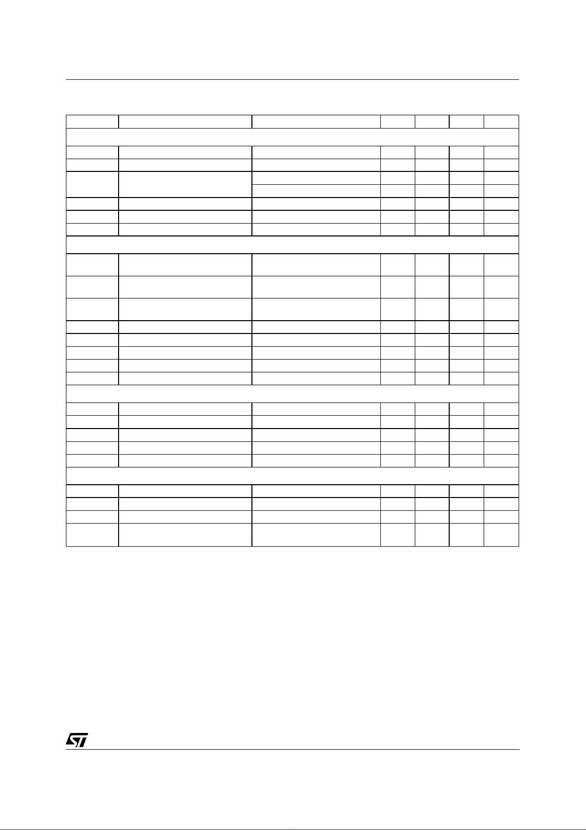
QUICK REFERENCE DATA
Symbol Parameter Min. Typ. Max. Unit
V
V
CL
THD Total Harmonic Distortion V = 1Vrms f = 1KHz 0.01 0.1 %
S/N Signal to Noise Ratio V
S
THERMAL DATA
Symbol Description Value Unit
R
th j-pins
ABSOLUTE MAXIMUM RATINGS
Supply Voltage 7 9 10.2 V
S
Max. input signal handling 2 Vrms
= 1Vrms (mode = OFF) 106 dB
out
Channel Separation f = 1KHz 90 dB
C
Treble Control (2db step) -14 +14 dB
Bass Control (2dB step) -14 +14 dB
Balance Control 1dB step (L
) -79 0 dB
CH, RCH
Mute Attenuation 100 dB
Thermal Resistance Junction-pins Max. 85 °C/W
Symbol Parameter Value Unit
V
T
amb
T
Operating Supply Voltage 11 V
S
Operating Ambient Temperature -10 to 85 °C
Storage Temperature Range -55 to +150 °C
stg
3/16

TDA7442 - TDA7442D
ELECTRICAL CHARACTERISTICS
(refer to the test circuit T
= 25°C, VS = 9V, RL = 10KΩ,
amb
Vin = 1Vrms; RG = 600Ω, all controls flat (G = 0dB), Effect Ctrl = -6dB, MODE = OFF; f = 1KHz
unless otherwise specified)
Symbol Parameter Test Condition Min. Typ. Max. Unit
SUPPLY
V
S
I
S
SVR Ripple Rejection LCH / R
Supply Voltage 7 9 10.2 V
Supply Current 10 18 26 mA
, Mode = OFF 60 80 dB
CH out
INPUT STAGE
C
RANGE
A
A
A
R
IN
V
CL
VMIN
VMAX
STEP
Input Resistance 35 50 65 KΩ
Clipping Level THD = 0.3% 2 2.5 Vrms
Control Range 31.5 dB
Min. Attenuation -1 0 1 dB
Max. Attenuation 31 31.5 32 dB
Step Resolution 0.5 1 dB
BASS CONTROL
Gb Control Range Max. Boost/cut +11.5 +14.0 +16.0 dB
B
STEP
R
B
Step Resolution 1 2 3 dB
Internal Feedback Resistance 32 44 56 KΩ
TREBLE CONTROL
Gt Control Range Max. Boost/cut +13.0 +14.0 +15.0 dB
T
STEP
Step Resolution 1 2 3 dB
EFFECT CONTROL
C
RANGE
S
STEP
Control Range - 21 - 6 dB
Step Resolution 0.5 1 1.5 dB
SURROUND SOUND MATRIX PHASE
R
R
R
R
PS10
PS11
PS12
PS13
Phase Shifter 1: D1 = 0, D0 = 0 8.3 11.8 15.2 KΩ
Phase Shifter 1: D1 = 0, D0 = 1 10 14.1 18.3 KΩ
Phase Shifter 1: D1 = 1, D0 = 0 12.6 17.9 23.3 KΩ
Phase Shifter 1: D1 = 1, D0 = 1 26.4 37.3 48.85 KΩ
SURROUND SOUND MATRIX
TEST CONDITION (Phase Resistor Selection D0=0, D1=1, D2=0. D3=1, D4=0, D5=1, D6=0, D7=1
Symbol Parameter Test Condition Min. Typ. Max. Unit
G
D
OFF
GOFF
In-phase Gain (OFF) Mode OFF, Input signal of
LR In-phase Gain Difference
(OFF)
G
MUS
D
GMUS
In-phase Gain (Music) Music mode, Effect Ctrl = -6dB
LR In-phase Gain Difference
(Music)
1kHz, 1.4 V
L
→ L
in
out
, Rin → R
p-p
out
Mode OFF, Input signal of
1kHz, 1.4 V
R
→ R
in
Input signal of 1kHz, 1.4 V
(Rin → R
p-p
, L
out
in
), (Lin → L
out
→ L
out
out
p-p
)
Music mode, Effect Ctrl = -6dB
Input signal of 1kHz, 1.4 V
(Rin → R
) - (Lin → L
out
out
p-p
)
-1 0 1 dB
-1 0 1 dB
7dB
0dB
4/16
TDA7442 - TDA7442D
ELECTRICAL CHARACTERISTICS
(continued)
Symbol Parameter Test Condition Min. Typ. Max. Unit
SPEAKER ATTENUATORS
C
S
V
A
R
range
STEP
E
A
DC
MUTE
VEA
Control Range 79 dB
Step Resolution -0.5 1 1.5 dB
Attenuation set error Av = 0 to -20dB -1.5 0 1.5 dB
Av = -20 to -79dB -3 0 2 dB
DC Steps adjacent att. steps -3 0 3 mV
Output Mute Condition +70 100 dB
Input Impedance 21 30 39 KΩ
AUDIO OUTPUTS
N
O(OFF)
N
O(MUS)
N
O(PSEUDO)
d Distorsion Av = 0 ; V
S
C
V
OCL
R
OUT
V
OUT
Output Noise (OFF) Output Mute, Flat
B
= 20Hz to 20KHz
W
Output Noise (Music) Mode = Music ,
B
= 20Hz to 20KHz,
W
Output Noise (Pseudo Stereo) Mode = Pseudo Stereo
B
= 20Hz to 20KHz,
W
= 1Vrms 0.01 0.1 %
in
4
5
30 mVrms
30 mVrms
Channel Separation 70 90 dB
Clipping Level d = 0.3% 2 2.5 Vrms
Output Resistance 10 30 50 Ω
DC Voltage Level 3.8 V
µVrms
µVrms
MONITOR OUTPUTS
d Distorsion Av = 0 ; Vin = 1Vrms 0.01 0.1 %
S
C
V
OCL
R
OUT
V
OUT
Channel Separation 70 90 dB
Clipping Level d = 0.3% 2 2.5 Vrms
Output Resistance 20 50 70 Ω
DC Voltage Level 4.5 V
BUS INPUT S
V
IL
V
IH
I
IN
V
O
Input Low Voltage 1 V
Input High Voltage 3 V
Input Current -5 +5 µA
Output Voltage SDA
IO = 1.6mA 0.4 V
Acknowledge
5/16

TDA7442 - TDA7442D
2
I
C BUS INTERFACE
Data transmission from microprocessor to the
TDA7442D and viceversa takes place through the
2 wires I
2
C BUS interface, consisting of the two
lines SDA and SCL (pull-up resistors to positive
supply voltage must be connected).
Data Validity
As shown in fig. 3, the dat a on the SDA line must
be stable during the high period of the clock. The
HIGH and LOW state of the data line can only
change when the clock signal on the SCL line is
LOW.
Start and Stop Conditions
As shown in fig.4 a start condition is a HIGH to
LOW transition of the SDA line while SCL is
HIGH. The stop condition is a LOW to HIGH transition of the SDA line while SCL is HIGH.
Byte Fo rmat
Every byte transferred on the SDA line must con-
tain 8 bits. Each byte must be followed by an ac-
2
Figure 3:
Data Validity on the I
CBUS
knowledge bit. The MSB is transferred first.
Acknowledge
The master (µP) puts a resistive HIGH level on the
SDA line dur ing the acknowle dge clock puls e (see
fig. 5). The peripheral (audioprocessor) that acknowledge s has to p ull-down ( LOW) the SDA li ne
during this clock pulse.
The audioprocessor which has been addressed
has to generate an acknowledge after the reception of each byte, otherwise the SDA line remains
at the HIGH level during the ninth clock pulse
time. In this case the master transmitter can generate the STOP information in order t o abort the
transfer .
Transmission without Acknowledge
Avoiding to detect the acknowledge of the audio-
processor, the µP can use a simpler transmission:
simply it waits one clock without checking the
slave acknowledging, and sends the new data.
This approach of course is less protected from
misworking.
Figure 4:
F
igure 5:
SDA
SCL
DATA LINE
STABLE, DATA
VALID
2
Timing Diagram of I
SCL
SDA
CBUS
START
Acknowledge on the I2CBUS
SCL
SDA
START
1
MSB
CHANGE
DATA
ALLOWED
D99AU1032
23789
D99AU1033
D99AU1031
2
I
CBUS
STOP
ACKNOWLEDGMENT
FROM RECEIVER
6/16

TDA7442 - TDA7442D
SOFTWARE SPECIFICA TION
Interface Protocol
The interface protocol comprises:
A start condition (S)
address
A subaddress bytes
A sequence of data (N byte + achnowledge)
A stop condition (P)
A chip address byte, containing the TDA7442D
CHIP ADDRESS
MSB
S 1 0 0 0 0 0 A 0 ACK ACK DATA ACK P
D95AU226A
LSB MSB LSB MSB LSB
SUBADDRESS DATA 1 to DATA n
B DATA
ACK = Achnowledge
S = Start
P = Stop
A = Address
B = Auto Increment
EXAMPLES
No Incremental Bus
The TDA7442D receives a start condition, the
correct chip address, a subaddress with the MSB
= 0 (no incremental bus), N-datas (all these datas
concern the subaddress selected), a stop condition.
CHIP ADDRESS
MSB
S 1 0 0 0 0 0 A 0 ACK ACK DATA ACK P
D95AU306
LSB MSB LSB MSB LSB
Incremental Bus
The TDA7442D receive s a start condition, the
correct chip address, a subaddress with the MSB
= 1 (incremental bus): now it is in a loop condition
with an autoincrease of the subaddress whereas
CHIP ADDRESS
MSB
S 1 0 0 0 0 0 A 0 ACK ACK DATA ACK P
D95AU307
LSB MSB LSB MSB LSB
SUBADDRESS DATA
XXX
0D3
D2 D1 D0
SUBADDRESS from "1XXX1010" to "1XXX1111"
of DATA are ignored.
The DATA 1 concern thesubaddress sent, and
the DATA 2 concern the subaddress sent plus
one in the loop etc, and at the end it receivers the
stop condition.
SUBADDRESS DATA 1 to DATA n
XXX
1D3
D2 D1 D0
7/16

TDA7442 - TDA7442D
DATA BYTES
Address = 80(HEX)
FUNCTION SELECTION:
The first byte (subaddress)
MSB LSB SUBADDRESS
D7 D6 D5 D4 D3 D2 D1 D0
BXXX0000INPUT ATTENUATION
BXXX0001SURROUND & OUT & EFFECT
BXXX0010PHASE RESISTOR
BXXX0011BASS
BXXX0100TREBLE
BXXX0101SPEAKER ATTENUATION "L"
BXXX0110SPEAKER ATTENUATION "R"
BXXX0111NOT ALLOWED
BXXX1000NOT ALLOWED
BXXX1001INPUT MULTIPLEXER
B = 1 incremental bus; active
B = 0 no incremental bus;
X = indifferent 0,1
CONTROL
INPUT ATTENUATION SELECTION
MSB LSB INPUT ATTENUATION
D7 D6 D5 D4 D3 D2 D1 D0 0.5 dB STEPS
10000
1 0 0 1 -0.5
1010-1
1 0 1 1 -1.5
1100-2
1 1 0 1 -2.5
1110-3
1 1 1 1 -3.5
4 dB STEPS
1000 0
1001 -4
1010 -8
1011 -12
1100 -16
1101 -20
1110 -24
1111 -28
INPUT ATTENUATION = 0 ∼ -31.5dB
8/16

TDA7442 - TDA7442D
SURROUND SELECTION
MSB LSB
D7 D6 D5 D4 D3 D2 D1 D0 SURROUND MODE
0 0 SIMULATED STEREO
0 1 MUSIC
1 0 OFF
OUT
0 VAR
1 FIX
EFFECT CONTROL
0000 -6
0001 -7
0010 -8
0011 -9
0100 -10
0101 -11
0110 -12
0111 -13
1000 -14
1001 -15
1010 -16
1011 -17
1100 -18
1101 -19
1110 -20
1111 -21
PHASE RESISTOR SELECTION
MSB LSB
D7 D6 D5 D4 D3 D2 D1 D0 PHASE SHIFT 1 (KΩ)
00 12
01 14
10 18
11 37
SURROUND PHASE
RESISTOR
9/16

TDA7442 - TDA7442D
BASS SELECTION
MSB LSB BASS
D7 D6 D5 D4 D3 D2 D1 D0 2 dB STEPS
XXX10000 -14
XXX10001 -12
XXX10010 -10
XXX10011 -8
XXX10100 -6
XXX10101 -4
XXX10110 -2
XXX10111 0
XXX11111 0
XXX11110 2
XXX11101 4
XXX11100 6
XXX11011 8
XXX11010 10
XXX11001 12
XXX11000 14
SPEAKER SELECTION
MSB LSB SPEAKER/ATT
D7 D6 D5 D4 D3 D2 D1 D0 1 dB STEPS
X0000
X001-1
X010-2
X011-3
X100-4
X101-5
X110-6
X111-7
8 dB STEPS
X0000 0
X0001 -8
X0010 -16
X0011 -24
X0100 -32
X0101 -40
X0110 -48
X0111 -56
X1000 -64
X1001 -72
MUTE
X101X
X11XX
X = INDIFFERENT 0,1
SPEAKER ATTENUATION = 0dB ∼ -79dB
10/16

TDA7442 - TDA7442D
TREBLE SELECTION
MSB LSB TREBLE
D7 D6 D5 D4 D3 D2 D1 D0 2 dB STEPS
00001110 -14
00011110 -12
00101110 -10
00111110 -8
01001110 -6
01011110 -4
01101110 -2
01111110 0
11111110 0
11101110 2
11011110 4
11001110 6
10111110 8
10101110 10
10011110 12
10001110 14
INPUT SELECTION
MSB LSB
D7 D6 D5 D4 D3 D2 D1 D0 INPUT MULTIPLEXER
X 0 0 0 IN2
X 0 1 0 IN3
X 1 0 0 IN4
X 1 1 0 IN1
POWER O N RESET
BASS 2dB
TREBLE 0dB
SURROUND & OUT CONTROL+ EFFECT CONTROL OFF + FIX + MAX ATTENUATION
SPEAKER ATTENUATION L &R MUTE
INPUT ATTENUATION MAX ATTENUATION
INPUT IN1
11/16

TDA7442 - TDA7442D
TREBLE- L , TR EB L E -R
PIN:
V
S
PIN:
VOUT REF
V
S
20µA
25K
GND
D95AU309
L-IN, R-IN, L-IN2, R-IN2, L-IN3, R-IN3,
PIN:
L-IN4, R-IN4,
V
S
20µA
PIN:
GND
CREF
GND
V
S
10K
20K
20µA
D95AU233A
20µA
42K
PIN:
GND
SCL, SDA
GND
50K
V
REF
D94AU200
PIN:
LP
V
S
20µA
D94AU205
GND
20K
D95AU336
GND
20µA
D95AU308
12/16

L-OUT, R-OUT
PIN:
TDA7442 - TDA7442D
BASS-LI, BASS-RI
PIN:
V
S
V
S
GND
BASS-LO, BASS-RO
PIN:
GND
20µA
GND
BASS-LO
D95AU230
V
S
20µA
45K
BASS-RO
45K
20µA
: Bass
D98AU949
BASS-LI,BASS-RI
D98AU950
13/16

TDA7442 - TDA7442D
DIM.
MIN. TYP. MAX. MIN. TYP. MAX.
A 2.65 0.104
a1 0.1 0.3 0.004 0.012
b 0.35 0.49 0.014 0.019
b1 0.23 0.32 0.009 0.013
C 0.5 0.020
c1 45° (typ.)
D 17.7 18.1 0.697 0.713
E 10 10.65 0.394 0.419
e 1.27 0.050
e3 16.51 0.65
F 7.4 7.6 0.291 0.299
L 0.4 1.27 0.016 0.050
S8° (max.)
mm inch
OUTLINE AND
MECHANICAL DATA
SO28
14/16

TDA7442 - TDA7442D
mm inch
DIM.
MIN. TYP. MAX. MIN. TY P. MAX.
A 3.556 3.759 5.080 0.14 0.147 0.2
A1 0.508 0.020
A2 3.048 3.556 4.572 0.12 0.14 0.18
B 0.356 0.457 0.584 0.014 0.018 0.023
B1 0.762 1.016 1.397 0.03 0.04 0.055
C 0.203 0.254 0.356 0.008 0 .01 0.014
D 27.43 27.94 28.45 1.08 1.1 1.12
E 9.906 10.41 11.05 0.39 0.409 0.433
E1 7.620 8.890 9.398 0.3 0.35 0.37
e 1.778 0.070
eA 10.16 0.400
eB 12.70 0.500
L 2.540 3.048 3.810 0.1 0.12 0.15
OUTLINE AND
MECH ANICAL DAT A
SDIP32
(Shrink Plastic Dip 32L)
B eB1
32
1
E
E1
A2
A
A1
D
17
16
L
eA
eB
C
SDIP32M
0123183
15/16

TDA7442 - TDA7442D
Information furnishe d is beli eved to be accu rate and reliable. However, STMicroelec tronics assumes no res ponsibility for the consequences
of use of such i nformation nor for any i nfringement of patents or ot her rights of third par ties which may result from its use. No license i s
granted by impli cation or otherwis e under any patent or patent righ ts of STMicroelect ronics. Specifica tion mentioned in this publication are
subject to change without notic e. This public ation supers edes and replaces all information prev iously supplied. STMic roelec tronic s products
are not authorized for use as critical components in life support devices or systems without express written approval of STMicroelectronics.
The ST logo is a registered trademark of STMicroelect roni cs
© 2001 STMicroelectronics – Printed in Italy – All Rights Reserved
STMicroelectronics GROUP OF COMPANIES
Australia - Brazil - Canada - China - Finland - France - Germany - Hong Kong - India - Israel - Italy - Japan - Malaysia - Malta - Morocco -
Singapore - Spain - Sweden - Switzerland - United Kingdom - United States.
http://www.st.com
16/16
 Loading...