

.
OPERATINGVOLTAGE1.8 TO 15 V
.
LOW QUIESCENTCURRENT
.
HIGH POWERCAPABILITY
.
LOW CROSSOVERDISTORTION
.
SOFT CLIPPING
TDA7231A
1.6WAUDIOAMPLIFIER
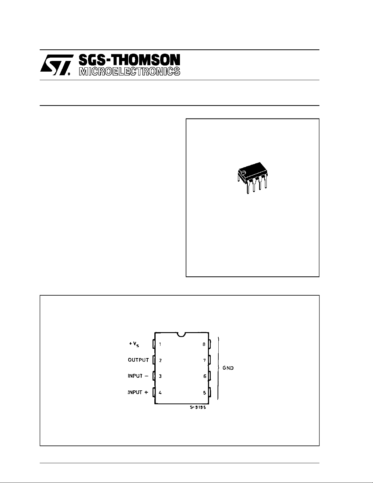
MINIDIP (4+4)
DESCRIPTION
TheTDA7231Aisa monolithicintegrated circuit in
4 + 4 lead minidip package. It is intended for use
as class AB power amplifier with wide range of
supply voltage in portable radios, cassette recordersand players, etc.
PIN CONNECTION
ORDERING NUMBER : TDA7231A
March 1995
1/5
TDA7231A
ABSOLUTE MAXIMUM RATINGS
Symbol Parameter Value Unit
V
s
P
tot
I
o
T
stg,Tj
THERMALDATA
Symbol Parameter Value Unit
R
th j-amb
R
th j-pins
Supply Voltage 16 V
Total Power Dissipation at T
at T
amb
case
=50°C
=70°C
1.25
4
Output Peak Current 1 A
Storage and Junction Temperature – 40 to 150 °C
Thermal Resistance Junction-ambient Max. 80 °C/W
Thermal Resistance Junction-pins Max. 15 °C/W
W
W
ELECTRICALCHARACTERISTICS (Vs= 6V,T
= 25 °C, unless otherwisespecified)
amb
Symbol Parameter Test Conditions Min. Typ. Max. Unit
V
s
V
o
I
d
I
b
P
o
d Distortion P
G
v
R
in
e
N
SVR Supply Voltage Rejection f = 100Hz, R
Supply Voltage 1.8 15 V
Quiescent Out Voltage VS=6V
=3V
V
S
2.7
1.2
Quiescent Drain Current 3.6 9 mA
Input Bias Current 100 nA
Output Power d = 10% f = 1kHz
= 12V RL=8Ω
V
s
=9V RL=4Ω
V
s
=6V RL=8Ω
V
s
=6V RL=4Ω
V
s
=3V RL=4Ω
V
s
=3V RL=8Ω
V
s
= 0.2 W
o
f = 1 kHz
=8Ω
R
L
1.8
1.6
0.4
0.7
110
70
0.3 %
Closed Loop Voltage Gain 38 dB
Input Resistance f = 1kHz 100 kΩ
Total Input Noise Rs= 10kΩ B = Curve A
B = 22Hz to 22kHz
= 10kΩ 24 33 dB
g
2
3
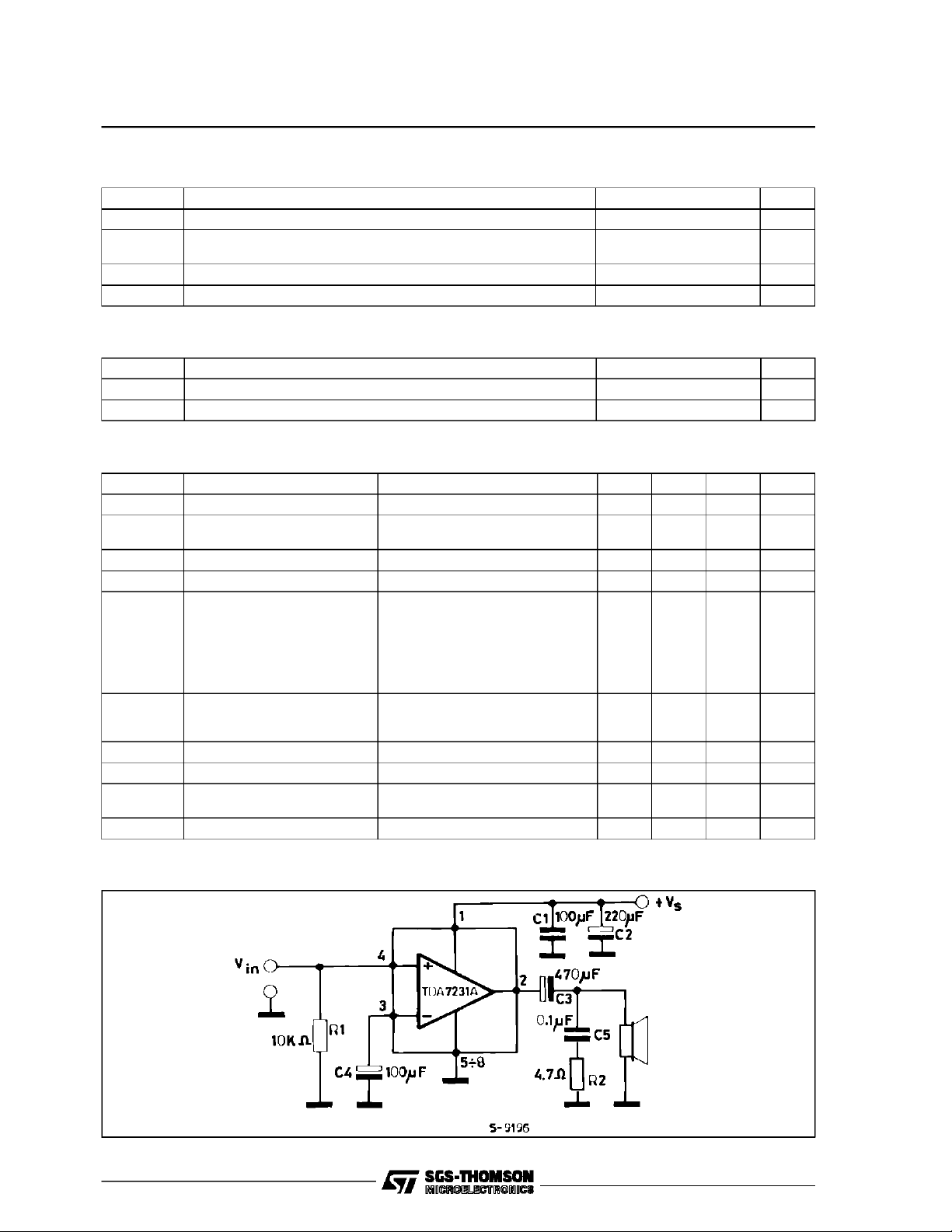
Figure1 : Testand ApplicationCircuit
V
V
W
W
W
W
mW
mW
µV
µV
2/5

Figure2 : P.C.Board and ComponentsLayout of thefigure 1 (1:1 scale)
TDA7231A
Figure3 : Output Power versus SupplyVoltage
Figure5 : Quiescent Output Voltageversus
Supply Voltage
Figure 4 : QuiescentCurrent versus
Supply Voltage
Figure 6 : SupplyVoltage Rejectionversus
Frequency
3/5

TDA7231A
MINIDIPPACKAGE MECHANICAL DATA
DIM.
MIN. TYP. MAX. MIN. TYP. MAX.
A 3.3 0.130
a1 0.7 0.028
B 1.39 1.65 0.055 0.065
B1 0.91 1.04 0.036 0.041
b 0.5 0.020
b1 0.38 0.5 0.015 0.020
D 9.8 0.386
E 8.8 0.346
e 2.54 0.100
e3 7.62 0.300
e4 7.62 0.300
F 7.1 0.280
I 4.8 0.189
L 3.3 0.130
Z 0.44 1.6 0.017 0.063
mm inch
4/5

TDA7231A
Information furnished is believed to be accurateand reliable. However, SGS-THOMSON Microelectronics assumes no responsibility for the
consequences of useof such information nor for any infringement of patents or other rightsof third parties whichmay result from itsuse. No
license is granted by implicationor otherwise underany patentorpatent rights ofSGS-THOMSON Microelectronics. Specifications mentioned
in this publication are subject to change without notice. This publication supersedes and replaces all information previously supplied.
SGS-THOMSON Microelectronics products arenotauthorized for useas critical components inlife supportdevices or systemswithout express
written approval of SGS-THOMSON Microelectronics.
1995 SGS-THOMSON Microelectronics - All Rights Reserved
Australia- Brazil - France - Germany- Hong Kong - Italy - Japan - Korea- Malaysia -Malta - Morocco - The Netherlands - Singa-
pore - Spain- Sweden - Switzerland - Taiwan - Thaliand - United Kingdom -U.S.A.
SGS-THOMSON Microelectronics GROUPOF COMPANIES
5/5
 Loading...