

TDA4605
CONTROLCIRCUIT FOR SWITCH MODE POWER SUPPLIES
USING MOS TRANSISTORS
.
FOLD-BACK CHARACTERISTIC PROVIDES
OVERLOAD PROTECTION FOR EXTERNAL
DIODES
.
BURST OPERATION UNDER SHORT-CIRCUIT AND NO LOADCONDITIONS
.
LOOP ERRORPROTECTION
.
SWITCH-OFF IN CASE OF TOO LOW LINE
VOLTAGE(under voltage switch-off)
.
LINE VOLTAGE COMPENSATION OF OVERLOADPOINT
.
SOFT-STARTFOR SMOOTH START-UP
.
CHIP OVER-TEMPERATURE PROTECTION
(thermalshutdown)
.
ON-CHIP PARASITIC TRANSFORMER OSCILLATIONSUPPRESSIONCIRCUITRY
.
DECREASE OF REGULATED VOLTAGE FOR
LOW POWERCONSUMPTION
ORDER CODE : TDA4605
DIP8
(Plastic Package)
DESCRIPTION
The ICTDA4605controlstheMOSPowerTransistor and performs all necessary regulation and
monitoring functions in free running flyback converters. Since good load regulation over a wide
load rangeisattained,thisICis particularlysuitable
for ConsumeraswellasIndustrialPowerSupplies.
Alternative source of the TDA4605 is also available from SIEMENS Semiconductors Consumer
ElectronicsA.G.
PINCONNECTIONS
REGULATION INPUT
PRIMARY CURRENT SIMULATION
PRIMARY VOLTAGE MONITORING
GROUND OUTPUT
1
2
3
4
SO8
(Plastic Micropackage)
ORDER CODE : TDA4605D
8
7
6
5
ZERO CROSSING DETECTOR INPUT
SOFT-START
SUPPLY VOLTAGE
April 1996
4605-01.EPS
1/6
TDA4605
PIN CONFIGURATION
Pin
Number
1 Regulating voltage : informationinput concerning secondary voltage.
By comparingthe regulating voltage obtainedfrom the regulating winding of the transformer with the
internal reference voltage, the output pulse width on Pin 5 is adaptedto the load of the secondary side
(normal, overload, short circuit, no load)
2 Primary currentsimulation : information input regarding the primary current. The primary current rise in the
primary winding is simulated at Pin 2 as a voltage riseby means of external RC element. When a value is
reached that is derived from the regulating voltage at Pin 1, the output pulse atPin 5 is terminated.The
RC element serves to set the maximum power at the overload point.
3 Primary voltagedetector : input for primary voltage monitoring.When the line voltage is too low the IC is
switched-off by comparing V
compensation.
with an internal reference. Voltage at Pin 3 is used for overload point
3
4 Ground
5 Output : push-pull output for charge and discharge of the gate capacitance of the power MOS transistor.
6 Supply voltage : Supply voltageinput. From it are derived a stable internal reference voltage (V
the switching threshold V
6>V6E
the V
REF
if V
V
6 min<V6<V6 max
6A,V6E,V6 max
isswitched on andswitched offwhen V6<V6A. In addition the logic is only enablefor
.
7 Soft-start : input forsoft-start and integration network. Start-up willbegin with short pulses by connecting a
capacitor between Pin 7 to ground. This capacitor together with a resistor connected between Pin 7and
error amplifier output also as acts an integrator network for regulation.
8 Zero detector : Input for theoscillator feedback. After starting oscillator, every zero transit of the feedback
voltage (falling edge) triggersan output pulse at Pin 5.The trigger threshold is at typically - 50mV
and V
Description
for thesupply voltage detector.
6 min
REF
) and
4605-01.TBL
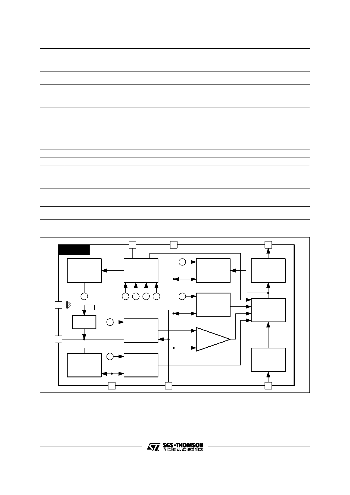
BLOCK DIAGRAM
TDA4605
Reference
Volta ge
(typ. 3V)
4
Current
S ourc e
1
Overload
Point
Correction
2
S upply
Voltage
V
2B
Monitor
V
REF
V
V
6min
V
V
6ma x
6E
6A
V
st
Primary
Current
Re copy
Sta rting
Impulse
Generator
R
Regulating
&Overload
Amplifier
Stop
Comp.
V
56
Output Sta ge
and
Current Limit
Logic
Zero
u
Low Voltage
Protection
V
Crossing
Detector
Monitoring
3
78
4605-02.EPS
2/6

TDA4605
ABSOLUTE MAXIMUM RATINGS
Symbol Parameter Pin Value Unit
V
1
V
2
V
3
Supply Voltage
V
4
V
6
V
7
I
1
I
2
I
3
I
I
I
I
I
T
T
stg
Supply Current
4
5
6
7
8
JunctionTemperature (autom. thermaldisjunction) +125
j
Storage Temperature -40, +125
t
≤50µs, V ≤ 0.1 4 - 1.5 A
p
tp≤ 50µs, V ≤ 0.1 5 -0.5, +1.5 A
tp≤ 50µs, V ≤ 0.1 6 0.5 A
THERMALDATA
Symbol Parameter Value Unit
R
R
th(j-a)
th(j-c)
T
Junction-ambient Thermal Resistance 80
Junction-case Thermal Resistance 45
Ambient Temperature -20, +85
amb
1 -0.3, +3 V
2 -0.3 V
3 -0.3 V
4 -0.3 V
6 -0.3, +20 V
7 -0.3 V
13mA
23mA
33mA
73mA
8 -3, +3 mA
o
C/W
o
C/W
o
C
o
C
4605-02.TBL
o
C
4605-03.TBL
ELECTRICAL CHARACTERISTICS (VCC= 10V,T
=25oC, unlessotherwisespecified)
amb
Symbol Parameter Test Conditions Min. Typ. Max. Unit
START-UP HYSTERESIS
I
V
V
I
I
6E0
6E1
6A1
Start-upCurrent Drain V6=V
Switch-on Voltage 11 12 13 V
6E
Switch-off Voltage 4.5 5 5.5 V
6A
Switch-on Current V6=V
Switch-off Current V6=V
VOLTAGE CLAMP (V
V
2(Max.)
V
3(Max.)
At Pin 2 (V6<V6E)I
At Pin 3 (V6<V6E)I
= 10V, IC Switched off)
6
6E
6E
6A
= 1mA 5.6 6.6 9 V
2
= 1mA 5.6 6.6 9 V
3
0.6 0.8 mA
11 mA
10 mA
CONTROL RANGE
V
-V
ControlInput Voltage 400 410 420 mV
1R
VoltageGain of the Control Circuit in the Control
R
Range
VR= d(V2S-V2B)/dV
f = 1kHz
1
43 dB
PRIMARY CURRENT SIMULATION VOLTAGE
V
Basic Value 0.955 1.00 1.03 V
2B
OVERLOAD RANGE AND SHORT CIRCUIT OPERATION
V
DV
V
Peak Value in the Range of Secondary Overload V1=V1R- 10mV 2.8 2.95 3.1 V
2O
Maximum Ramp Amplitude V2O-V
2
Peak Value in the Range of Secondary Short
2S
Circuit Operation
2B
V1= 0 2.3 2.5 2.7 V
1.82 1.95 2.08 V
FOLDBACK POINT CORRECTION
-I
Foldback Point Correction Current V3= 3.7V 300 500 650 µA
2
4605-04.TBL
3/6

TDA4605
ELECTRICAL CHARACTERISTICS (VCC= 10V,T
=25oC, unlessotherwisespecified)(continued)
amb
Symbol Parameter Test Conditions Min. Typ. Max. Unit
GENERALLY VALID DATA (V
VOLTAGE OF THE ZERO TransitionDETECTOR
V
V
V
Positive Clamping Voltage I8= 1mA 0.75 V
8P
Negative Clamping Voltage I8= -1mA -0.2 V
8N
ThresholdValue 40 50 mV
8S
= 10V)
6
TUL Suppression of Transformer Ringing 3 3.8 4.5 µs
-I
InputCurrent V8=0 0 4 µV
8
PUSH-PULL OUTPUT STAGE
SATURATION VOLTAGES
V
V
V
SatU
SatU
SatU
Pin 5 Sourcing I5= -0.1A 1.5 2.0 V
Pin 5 Sinking I5= +0.1A 1.0 1.2 V
Pin 5 Sinking I5= +0.5A 1.4 1.8 V
OUTPUT SLOW RATE
+dV
/dt Rising Edge 70 V/µs
5
-dV
/dt Falling Edge 100 V/µs
5
REDUCTION OF CONTROL VOLTAGE
-I
Current to reduce the Control Voltage V7=1V 50 µA
1
PROTECTION CIRCUIT
V
6(Min.)
V
6(Max.)
V
Undervoltage Protection for V6:
Voltage at Pin 5 = V
Overvoltage Protection for V6:
Voltage at Pin 5 = V
Undervoltage Protection for VAC:
3A
Voltage at Pin 5 = V
5(Min.)
5(Min.)
5(Min.)
if V6<V
if V6>V
if V3<V
6(Min.)
6(Max.)
3A
Oj Over Temperature : at the given chip temperature the
IC will switch V
V
Voltageat Pin 3 if one of theprotection functions was
3Sat
triggered ; (V
Current Drain during Burst Operation V3=V2=0V 8 mA
I
6
to V
5
5(Min.)
will be clamped until V6<V6A)
3
V2= 0V 970 1005 1040 mV
I
= 750µA 0.4 0.8 V
3
7.0 7.25 7.5 V
15 16 16.5 V
150
o
C
4605-05.TBL
FUNCTIONAL DESCRIPTION
In free running fly-back converters, the TDA4605
assumescontrolofa MOS power transistorand all
necessaryregulationand monitoring functions.
The serial circuit of power transistor and primary
windingof the flyback transformeris connected to
theinputvoltage.Duringtheswitch-onperiodofthe
transistor, energy is stored in the transformerand
during the switch-off period it is fed to te load via
the secondary winding. By varing the switch-on
time of the power transistor, the IC controls each
portionofenergytransferredtothesecondaryside
such that the output voltage remains nearly independentof load variations.
The requiredcontrol informationis taken from the
input voltage during the switch-onperiodand from
a regulationwindingduring the switch-offperiod.A
new cyclebegins as soon as the energystored in
the transformer has been totally delivered to the
4/6
secondaryside.
In differentload ranges, the SMPS willbehave as
follows :
- No-Load Operation : The power supply unit
oscillates in non continuous mode at a typical
frequency of 20 to 40kHz. Depending upon the
transformer winding and the regulated voltage
divider, the output voltage can be slightly above
the nominalvalue.
- Normal Operation : Starting from typ. 200kHz,
the switchingfrequency falls withincreasingload
and decreasing AC voltage. The duty cycle depends primarily on the AC voltage. The output
voltage is only slightly load-dependent.
- OverloadPoint:Maximumoutputpowerisavailable at this point of the outputcharacteristics
- Overload:The energytransferredper operation
cycle is limited at the top. Therefore, the output
voltage will fall with secondaryoveloading.

PACKAGE MECHANICAL DATA
8 PINS- PLASTICDIP
TDA4605
PM-DIP8.EPS
Dimensions
Min. Typ. Max. Min. Typ. Max.
Millimeters Inches
A 3.32 0.131
a1 0.51 0.020
B 1.15 1.65 0.045 0.065
b 0.356 0.55 0.014 0.022
b1 0.204 0.304 0.008 0.012
D 10.92 0.430
E 7.95 9.75 0.313 0.384
e 2.54 0.100
e3 7.62 0.300
e4 7.62 0.300
F 6.6 0260
I 5.08 0.200
L 3.18 3.81 0.125 0.150
Z 1.52 0.060
DIP8.TBL
5/6

TDA4605
PACKAGE MECHANICAL DATA
8 PINS- PLASTICMICROPACKAGE (SO)
PM-SO8.EPS
Dimensions
Min. Typ. Max. Min. Typ. Max.
Millimeters Inches
A 1.75 0.069
a1 0.1 0.25 0.004 0.010
a2 1.65 0.065
a3 0.65 0.85 0.026 0.033
b 0.35 0.48 0.014 0.019
b1 0.19 0.25 0.007 0.010
C 0.25 0.5 0.010 0.020
c1 45
o
(Typ.)
D 4.8 5.0 0.189 0.197
E 5.8 6.2 0.228 0.244
e 1.27 0.050
e3 3.81 0.150
F 3.8 4.0 0.15 0.157
L 0.4 1.27 0.016 0.050
M 0.6 0.024
S8
Information furnished is believed tobe accurate and reliable. However,SGS-THOMSON Microelectronics assumes no responsibility
for the consequences of use of suchinformation nor forany infringementofpatents or other rights of third parties which may result
from its use.No licenceis granted by implication orotherwise under anypatent or patent rights ofSGS-THOMSON Microelectronics.
Specifications mentioned in this publication are subject to change without notice. This publication supersedes and replaces all
information previously supplied.SGS-THOMSON Microelectronicsproductsare not authorized for use as critical components in life
support devices or systems without express written approval of SGS-THOMSON Microelectronics.
1996 SGS-THOMSON Microelectronics - All Rights Reserved
Purchase of I
2
I
C Patent. Rights to use these components in a I2C system,is granted provided thatthe system conforms to
Australia - Brazil - China - France - Germany - Hong Kong - Italy -Japan - Korea - Malaysia - Malta- Morocco
The Netherlands - Singapore - Spain - Sweden - Switzerland -Taiwan - Thailand - United Kingdom - U.S.A.
2
C Components of SGS-THOMSON Microelectronics, conveys a license under the Philips
2
the I
C Standard Specificationsas defined by Philips.
SGS-THOMSON Microelectronics GROUPOF COMPANIES
o
(Max.)
SO8.TBL
6/6
 Loading...