

.
CHROMINANCE SIGNALPROCESSOR
.
LUMINANCE SIGNAL PROCESSING WITH
CLAMPING
.
HORIZONTALANDVERTICALBLANKING
.
LINEAR TRANSMISSION OF INSERTED
RGB SIGNALS
.
LINEAR CONTRAST AND BRIGHTNESS
CONTROLACTING ON INSERTED AND MATRIXEDSIGNALS
.
AUTOMATICCUT-OFF CONTROL
.
NTSCHUE CONTROL
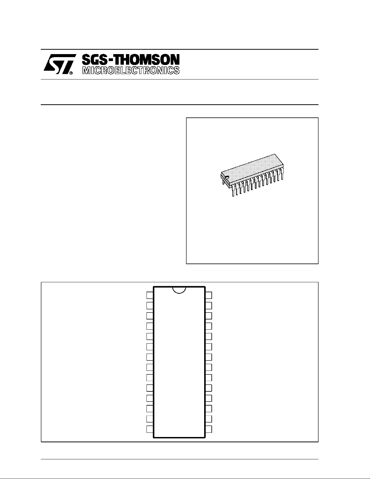
TDA3562A
PAL/NTSC ONE-CHIPDECODER
DIP28
(Plastic Package)
DESCRIPTION
The TDA3562A is a monolithic IC designed as
decode PALand/or NTSC colour television standards and it combines all functions required for the
identificationand demodulationof PALand NTSC
signals.
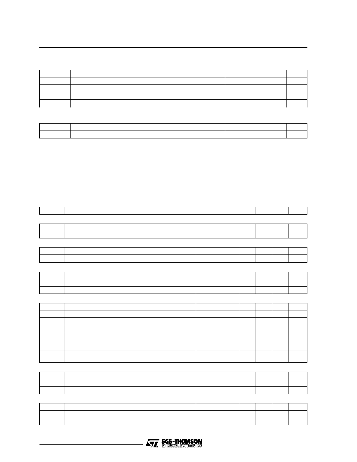
PINCONNECTIONS
COLOR IDENTIFICATION
CC
DETECTORCAPACITOR
PEAK DETECTORCAPACITOR
CHROMINANCEINPUT
SATURATION CONTROL
CONTRASTCONTROL
SUPERSCANDLEINPUT
LUMINANCEINPUT
FAST BLANKINGINPUT
CUT-OFFMEMORY(RED)
BRIGHTNESSCONTROL
RED EXTERNALINPUT
RED OUTPUT
1
2
3
4
5
6
7
8
9
10
11
12
13
28
27
26
25
24
23
22
21
20
19
18
17
16
ORDER CODE : TDA3562A
CHROMA OUTPUTV
GROUND
XTAL
PHASE DETECTOR OUTPUT
PHASE DETECTOR OUTPUT
R-Y DEMODULATORINPUT
B-Y DEMODULATORINPUT
CUT-OFFMEMORY (GREEN)
CUT-OFFMEMORY(BLUE)
LEAKAGECURRENT MEMORY
CATHODE CURRENT INPUT
BLUE OUTPUT
BLUE EXTERNAL INPUT
June 1993
GREEN EXTERNAL INPUT GREEN OUTPUT
14
15
3562A-01.EPS
1/9

TDA3562A
BLOCK DIAGRAM
CONTROL
BRIGHTNESS
CONTROL
CONTRAST
DATA
SWITCH
DATAINPUT
RG B
64µs
PALD.L.
R
20
17 B
116
BLUEMATRIXCONTRAST
CHARACTERSINSERTION
BRIGHTNESSCONTROLSB.L.CLAMP
12 14 16 9
B-Y
DEMODULATION
21
15 G
GREEN-CHANNEL
G-Y
MATRIX
10
13
RED-CHANNEL
R-Y
DEMODULATION
CUT-OFF
INPUTSENSE
18
CLAMP
CUT-OFF
VCO
90° SHIFT
PHASE
DETECTOR
1926
2/9
28 23 22
71
INPUT
SUPER
SANDCASTLE
+12V
DETECTOR
SANDCASTLE
B.L.CLAMP
Y AMPLIFIER
5
CONTROL
SATURATION
Y INPUT 6
BUFFER
CONTROL
SATURATION
GATEDAMPLIFIER
AMPLIFIER
CONTROLCHROMA
4
INPUT
CHANEL
PAL
FLIPFLOP
KILLER
GENERATOR
F.E.CORRECTION
AGCPEAK
DETECTOR
3
PAL
SWITCH
BURST
DETECTOR
COLOR
DETECTOR
IDENTIFICATION
2
NTSC
SHIFT
PAL(R-Y)
NTSC(B-Y)
REFERENCE
SWITCH
PAL/NTSC
27 23 24
3562A-02.EPS
TDA3562A
ABSOLUTE MAXIMUMRATINGS
Symbol Parameter Value Unit
V
S
P
tot
T
stg,Tj
T
amb
THERMALDATA
Symbol Parameter Value Unit
R
th j-amb
ELECTRICALCHARACTERISTICS
Test conditions unless otherwise specified: Supplyvoltage,Pin 1 at 12 V - T
Inputsignals : Luminance input signal V
Controlinputs at nominalvalue : Pin 6 Nom. contrast = max. contrast– 5dB
Symbol Parameter Test Conditions Min. Typ. Max. Unit
SUPPLY INPUT (pin 1)
LUMINANCE INPUT (pin 8)
CHROMINANCE INPUT (pin 4)
SUPER SANDCASTLE INPUT (pin7)
DATA BLANKING INPUT (pin 9)
”BLACK CURRENT” STABILIZATION INPUT (pin 18)
Supply Voltage 13.2 V
Power Dissipation at T
amb
=65°C
1.7 W
Storage and Junction Temperature – 25, +150 °
Ambient TemperatureRange 0, +70 °
Thermal Resistance Junction-ambient Max 40 °
=25°C
amb
= 0.48 VPP(Compositevideo signal(100 % white)
Chrominanceinputsignal V
8
= 0.39 VPP(Colourbar signalwith 75 % coloursaturation
4
and chrominance to burst ratio = 2.2 : 1)
Datainput signals V
12, 14, 16
=1.4 VPP(Includingneg.goingsync.pulse)
Pin 5 Nom.saturation = max. saturation– 6 dB
Pin 11 Nom. brightness = 2V,Pin 9 at 0.4 V
Supply Voltage Range 10.8 13.2 V
Supply Current V
Composite Input Signal 0.8 V
Input Current 0.1 1
Input Signal 40 1100 mV
Input Resistance 10
Input Capacitance 6.5 pF
Gating & Clamping Level 7.5 V
H-pulse Separating Level 4 5 V
V-pulse Separating Level 2 3 V
Forbidded Range 1 to 2 V
Input Current V
Delay Between Black Level Clamping Pulse and Gating
Pulse
Input Voltage forno Data Insertion 0.4 V
Input Voltage forData Insertion 0.9 3 V
Input Resistance 7 13
D. C. Bias Voltage 3.5 5 7 V
Internal Limiting Threshold 9 V
Switching Threshold for ”Black Current” ON 8 V
= 12 V 80 110 mA
1
= 0 to 1V
7
= 1 to 8.5V
V
7
= 8.5 to 12V
V
7
– 460
50
2
0.6 µ
C
C
C/W
pp
µA
KΩ
µA
µA
mA
s
kΩ
3562A-01.TBL
3562A-02.TBL
PP
3562A-03.TBL
3/9

TDA3562A
ELECTRICALCHARACTERISTICS (continued)
Symbol Parameter Test Conditions Min. Typ. Max. Unit
”BLACK CURRENT” STABILIZATION INPUT (pin 18) (continued)
Difference between Input Voltage for ”BlackCurrent”
and Leakage Current
InputResistance during Scan 1.5
InputCurrent during ”Black Current” Measurement 2 µ
InputCurrent during Scan 10 mA
RGB - OUTPUTS (Pins 13, 15, 17)
Output Resistance 50 Ω
Current Source 2 3 mA
Peak Output Level 10.7 11.3 V
Residual 4.4 MHz at RGB Outputs 100 mVpp
Residual 8.8 MHz at RGB Outputs 150 mVpp
LUMINANCE CHANNEL
Frequency Resp. of Total Lumin. Amplifiers f = 0 to 5MHz –1 –3 dB
RGB Output Signal (black to white) 3.5 4 4.5 Vpp
Relative Spread of RGB - Output Signals 1 dB
Contrast Control Range (see fig. 1) –5 to 10 dB
Tracking Over 10 dB Contrast Control 0 dB
Contrast Control Input Current 15 µ
Blanking Level of RGB -Output Signals 1 1.2 V
Difference Between Blanking Levels, 0 mV
Differential Drift of Blanking Levels ∆
Brightness Control Input Current 5 µ
Brightness Control Range (see fig. 3) 1 to 3 V
Relation Ship between Black Level Variation and
Brightness Control Variation
Black Level of RGB OutputSignals (see note 4) 3 V
Difference between Black Levels (see note 4) 0 mV
Tracking Over Brightness Control 2 %
Differential Drift of Black Levels ∆
Drift of Black Level Versus 10 % Variation of Supply
Voltageand Contrast Control
”CUT OFF CURRENT” REGULATION
RGB Output Level of the ”3L Windows” after Switchon
RGB Outputs Level of the ”3L Windows” after Cut
off Current Stabilization
RGB Output Range 1 5 V
Charge/Discharge Current during Measuring Time
(3L windows) at Pins 10, 19, 20 and21
Leakage Currents Flowing into Pins 10, 20 and 21
during Scan
RGB DATA INSERTION
Data RGB Output Signal V
Differential Amplitude Error between RGB Output
Signal and Data Output Signal
Differential Error between Black Levels of RGB
Output Signals and Black Levels of Data Output
Signals
T=40°C
(see fig. 3) 1.3 V/V
T=40°C
7.5 V
(see note 4) 1 3 5 V
= 0.9 to 3V 4 Vpp
9
0.5 V
0mV
20 mV
20 mV
1mA
50 nA
10 %
200 mV
kΩ
A
A
A
3562A-04.TBL
4/9

TDA3562A
ELECTRICALCHARACTERISTICS (continued)
Symbol Parameter Test Conditions Min. Typ. Max. Unit
RGB DATA INSERTION (continued)
Rise Time of Data Output Signal 50 80 ns
Differential Delay 0 40 ns
Attenuation of RGB Output Signal V
Frequency Response for f = 0 to 5 MHz – 1 – 3 dB
CHROMINANCE CHANNEL
Pin 4 Chrominance Input Signal 40 1100 mVpp
Pin 4 Input Resistance 10
Pin 4 Input Capacitance 6.5 pF
ACC Control Range 30 dB
PIn 28 Burst ChangeOver 30 dB ACC Range 1 dB
Saturation Control Range (see fig. 2) – 44
Pin 5 Sat. Control Input Current 20
Pin 28 Chrominance Output Voltage V
Burst Input Signal at Pins 22 and 23 100 mVpp
Input Resist. Bet. Pins 22, 23 and Ground 1
Pin 28 Phase Shift Bet. Burst and Chrom. Signal – 5 0 5 °
Pin 2 Voltage at Nom. Input Signal 4.7 V
Pin 2 Voltage without Input Signal 2.6 V
Pin 2 Identificaton-on Voltage 2.1 V
Pin 2 Colour-off Voltage 3.4 V
Pin 2 Colour-on Voltage 3.6 V
Pin 3 Voltage at Nom. Input Signal 5.1 V
COLOUR DEMODULATORS AND G-Y MATRIX
Ratio (B-Y) / (R-Y) 1.60 1.78 1.96
Ratio (G-Y) / (R-Y) (B – Y) = 0 – 0.46 – 0.51 – 0.56
Ratio (G-Y) / (B-Y) (R – Y) = 0 – 0.14 – 0.19 – 0.24
REFERENCE OSCILLATOR
Oscillator Frequency 2 fcs MHz
Temp. Coefficient of Oscillator Frequency (see note 5) – 2 Hz/k
Pin 26 Input Resistance 400
Pin 26 Input Capacitance 10 pF
Pull-in Range (see note 5) 500 700 Hz
Phase Shift for ±400 Hz Deviation
Phase Shift between (R – Y) and (R – Y)
Ref.Signal
Phase Shift between (R – Y) and (B – Y)
Ref.Signal
NTSC OPERATION
Pins 24, 25 PAL-on Operating Range 9 11 V
Pins 24, 25 Threshold for NTSC-on 8.8 V
J
24+J25
Avarage Output Current
Hue Control ±
Pins 24, 25 Hue Control Voltage 7.5 8.5 V
(4) The levelsdepend on the application circuit and on the spreadand drift of picture tube guns.
(5) All frequency variationsare referred to 4.4 MHzcarrier frequency.
= 0.9 to 3 V 46 dB
9
to 6
= 4.2 V 4 Vpp
5
5 °
5 °
85 90 95 °
Key Pulse = 4 µs
90 µ
30 °C
kΩ
dB
µA
kΩ
Ω
C
C
C
A
3562A-05.TBL
5/9

TDA3562A
Figure 1 : Contrast Control Voltage Range
G(%)
100
50
V
6-27
(V)
123450
Figure 3 : Difference betweensignalblack level
and measuringlevel (3L windows
after cut off current stabilization)
at theRGB outputs(∆V) versus
controlvoltage (V
11-V12
).
∆V (V)
2
1
Figure2 : SaturationControl VoltageRange
G (%)
100
50
3562A-03.EPS
123450
Figure4 : Hue Control Voltage Range
ϕ (deg)
60
40
20
V
5-27
(V)
3562A-04.EPS
0
-1
V
11-27
(V)
-2
01234
0
-20
-40
-60
3562A-05.EPS
V
24-25-27
(V)
7.5 8 8.5
3562A-06.EPS
6/9

Figure 5 : ApplicationDiagram showing theTDA3562Afora PALDecoder
TDA3562A
Ω
+12V
brightness
10k
+12V
470Ω
10nF
DL700
47kΩ
information
black current
Ω
10k
2.2µF
RB
82kΩ
RA
130kΩ
+12V
1kΩ
fosc adjust
1.2kΩ
120kΩ
average
beam
BAW62
12pF
4.7kΩ
current
68kΩ
8.8MHz
33kΩ
33kΩ33kΩ
1µF
+12V
3-level
sandcastle
10kΩ
47kΩ
red green blue
pulse
4.7µF
contrast
33nF
33nF
15kΩ
11 6
17
13 15
72618
22
25 24 23
3
28
+12V
saturation
68kΩ
100nF 100nF
100nF
470nF 470nF 10nF
1µF
330nF 470nF
10nF
Luminancedelay
22nF100µF
10kΩ
47kΩ
330nF
1kΩ 1kΩ
F
µ
15kΩ
2.2
Ω 75Ω
75
75Ω
Rext Gext Bext
Ω
75
blanking
27pF
46µH10.7
1kΩ
video
(1Vp-p)
composite
H
µ
120pF
2.2µF
8 91214 16 5
21
TDA3562A
10 20
19
27
42
1
+12V
unkiller
normal
killer
390Ω
+12V
3562A-07.EPS
7/9

TDA3562A
Figure 6 : ApplicationDiagram showing theTDA3562Afora PAL/NTSCDecoder
120kΩ
+12V
+12V
black current
B
A
(+PAL)
(+NTSC)
brightness
10kΩ
Ω
47k
information
RB
RA
130kΩ
+12V
contrast
current
68kΩ
8.8MHz
7.16MHz
47kΩ
blue
red green
3-level
sandcastlepulse
10kΩ
+12V
saturation
15kΩ
6
15 17 11
13
18
726
68kΩ
100nF 100nF
100nF
10kΩ
15kΩ
47kΩ
75Ω75Ω 75Ω 75Ω
2.2µF
Rext Gext Bext
blanking
46µH
1kΩ
2.2µF
5
12 14 16
9
8
20 21
56pF10kΩ
+12V
normal
unkiller
27pF
killer
22kΩ
TDA3562A
B
22
10
330nF
+12V
average
beam
Ω
10k
2.2µF
BAW62
82kΩ
22pF22pF
22kΩ
22kΩ
8/9
470Ω
DL700
390Ω
19
10nF 330nF 470nF1µF 470nF 470nF 10nF
4227
1
+12V
Luminancedelay
22nF100µF
1kΩ
video
(1Vp-p)
composite
1kΩ
µH
10.7
120pF
56pF10kΩ
22kΩ
B
+12V
3562A-08.EPS
33nF
100nF
4.7µF
23
32524
28
Ω1kΩ
10k
+12V
1kΩ
2.2kΩ
10nF
hue control
1.2kΩ
22kΩ
B
22kΩ
2.2kΩ
12kΩ
B
F
µ
2.2
10kΩ

PACKAGE MECHANICAL DATA
28 PINS- PLASTIC28
TDA3562A
I
L
E
28
114
Dimensions
a1
b
b2
e3
D
e
15
F
Millimeters Inches
Min. Typ. Max. Min. Typ. Max.
a1 0.63 0.025
b 0.45 0.018
b1 0.23 0.31 0.009 0.012
b2 1.27 0.050
D 37.4 1.470
E 15.2 16.68 0.598 0.657
e 2.54 0.100
e3 33.02 1.300
F 14.1 0.555
i 4.445 0.175
L 3.3 0.130
b1
PM-DIP28.EPS
DIP28.TBL
Information furnished is believed to beaccurate andreliable. However, SGS-THOMSON Microelectronicsassumes no responsibility
for the consequences of use ofsuch information norfor anyinfringement of patents or other rights of third partieswhich mayresult
from itsuse. Nolicence is granted by implication orotherwise under any patent orpatent rights of SGS-THOMSON Microelectronics.
Specifications mentioned in this publication are subject to change without notice. This publication supersedes and replaces all
information previously supplied. SGS-THOMSON Microelectronics productsare not authorized for use as critical components in life
support devices or systems without express written approval of SGS-THOMSON Microelectronics.
1994 SGS-THOMSON Microelectronics - All Rights Reserved
Purchase of I
2
I
C Patent. Rights to use these components in a I2C system, is granted provided that the system conforms to
Australia - Brazil - China - France - Germany - Hong Kong - Italy - Japan- Korea - Malaysia - Malta - Morocco
The Netherlands- Singapore - Spain - Sweden - Switzerland -Taiwan - Thailand - United Kingdom - U.S.A.
2
C Components of SGS-THOMSON Microelectronics, conveys a license under the Philips
2
the I
C Standard Specificationsas definedby Philips.
SGS-THOMSON Microelectronics GROUP OF COMPANIES
9/9
 Loading...