

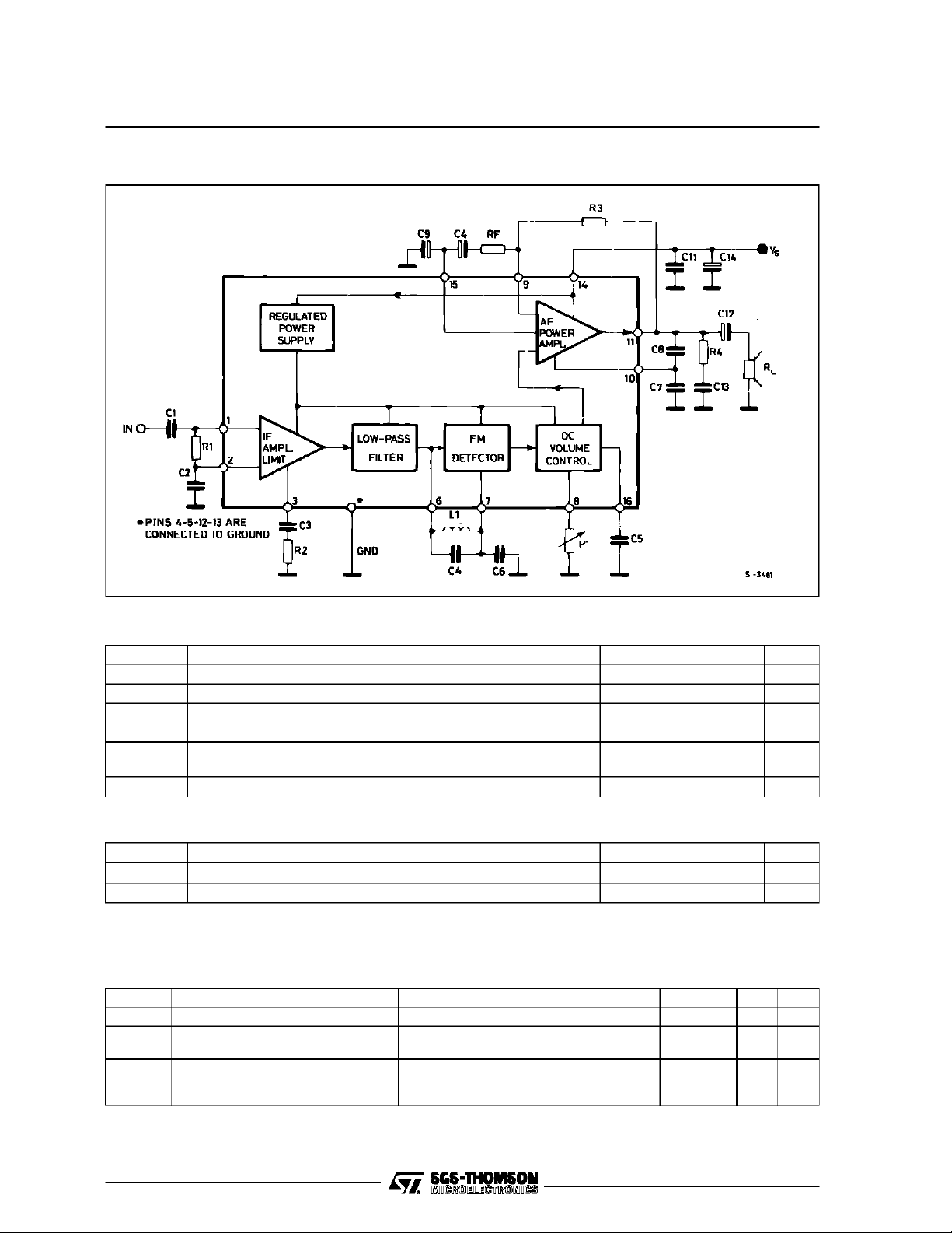
COMPLETE TV SOUND CHANNEL
The TDA3190is a monolithicintegratedcircuitin a
16-leaddual in-lineplastic package. Itperformsall
the functionsneededfor theTV soundchannel :
.
IF LIMITER AMPLIFIER
.
ACTIVELOW-PASSFILTER
.
FM DETECTOR
.
DC VOLUMECONTROL
.
AF PREAMPLIFIER
.
AF OUTPUT STAGE
DESCRIPTION
The TDA3190 can give an output power of 4.2 W
(d = 10 %) into a 16 Ω load at V
(d = 10 %) into an 8 Ω load at V
performance,togetherwiththeFM-IFsectionchar-
acteristicsofhigh sensitivity, highAMrejection and
low distortion, enables the device to be used in
almost everytype of televisionreceivers.
The device has no irradiation problems,hence no
externalscreening is needed.
The TDA3190 is a pin to pin replacement of
TDA1190Z.
=24 V,or 1.5 W
S
= 12 V. This
S
TDA3190
DIP16
(Plastic Package)
ORDER CODE : TDA3190
PINCONNECTIONS
December 1992
IF INPUT
IF DECOUPLING
IF DECOUPLING
GROUND
GROUND
FM DETECTOR
FM DETECTOR
DC VOLUMECONTROL
1
2
3
4
5
6
7
8
16
15
14
13
12
11
10
DE-EMPHASIS
RIPPLE REJECTION
SUPPLY VOLTAGE
GROUND
GROUND
AF OUTPUT
COMPENSATION
AF FEEDBACK
9
3190-01.EPS
1/9
TDA3190
BLOCK DIAGRAM
ABSOLUTE MAXIMUMRATINGS
Symbol Parameter Value Unit
V
V
I
I
P
T
stg,Tj
S
o
o
tot
Supply Voltage (pin 10) 28 V
Input Signal Voltage (pin 1) 1 V
i
Output Peak Current (non-repetitive) 2 A
Output Peak Current (repetitive) 1.5 A
Power Dissipation at T
at T
=90°C
pins
=70°C (freeair)
amb
4.3
1
Storage and Junction Temperature – 40 to 150
THERMALDATA
Symbol Parameter Value Unit
R
th j-pins
R
th j-amb
* Obtainedwith the GND pins soldered toprinted circuit with minimizedcopper area.
Thermal Resistance Junction-pins Max 14 °
Thermal Resistance Junction-ambient Max 80*
°C/W
ELECTRICAL CHARACTERISTICS
(refer to the test circuit, V
= 24V, T
S
Symbol Parameter Test Conditions Min. Typ. Max. Unit
V
Supply Voltage (Pin 14) 9 28 V
s
V
Quiescent Output Voltage (Pin11) Vs= 24V
o
I
Quiescent Drain Current
d
=25oC unlessotherwisespecified)
amb
= 12V
V
s
= 22kΩ
P
1
= 24V
V
s
= 12V
V
s
11
5.1
11 22
12
19
6
6.9VV
4540mA
13
W
W
°C
C/W
mA
3190-02.EPS
3190-01.TBL
3190-02.TBL
3190-03.TBL
2/9
TDA3190
ELECTRICAL CHARACTERISTICS
(refer to the test circuit, V
= 24V, T
S
Symbol Parameter Test Conditions Min. Typ. Max. Unit
Po Output Power d = 10%,f
Input Limiting Voltage (–3dB)
V
i
atPin 1
d Distortion P
B Frequency Response of audio
amplifier (–3dB)
V
Recovered Audio Voltage(Pin16)
o
AMR Ampliture Modulation Rejection
S + N
Signal to Noise Ratio
N
R
External Feedback Resistance
3
(betweenPins9and11)
R
Input Resistance (Pin1) Vi= 1mV, fo = 4.5MHz 30
i
C
Input Capacitance (Pin1) 5 pF
i
SVR Supply Voltage Rejection
DC Volume ControlAttenuation
A
v
=25oC unlessotherwisespecified)
amb
= 400Hz,
f
= 4.5MHz, ∆f=±25kHz
o
d = 2%, f
f
= 4.5MHz, ∆f=±25kHz
o
= 4.5MHz, ∆f=±7.5kHz,
f
o
f
m
o
f
= 4.5MHz, ∆f=±7.5kHz
o
R
L
C
7
V
i
f
m
V
i
f
m
V
I
f
m
R
L
P
1
P
1
m
V
= 24V, RL=16Ω
s
V
= 12V, RL=8Ω
s
= 400Hz,
m
= 24V, RL=16Ω
V
s
V
= 12V, RL=8Ω
s
= 400Hz, P1=0
= 50mW, fm= 400Hz,
= 24V, RL=16Ω
V
s
V
= 12V, RL=8Ω
s
=16Ω,C8= 120pF
= 470pF, P1= 22kΩ
=82Ω
R
f
R
=47Ω
f
≥ 1mV, fo= 4.5MHz
= 400Hz, ∆f=±7.5kHz, P1=0
≥ 1mV, fo= 4.5MHz,
= 400Hz, ∆f= ± 25kHz,m = 0.3
≥ 1mV, Vo= 4V, fo= 4.5MHz,
= 400Hz, ∆f=±25kHz
=16Ω,f
ripple
= 120Hz,
= 22kΩ
= 12kΩ
4.2
1.5
3.5
1.4
40 100
0.75
1
70 to 1200
70 to 7000
120 mV
55 dB
50 65 dB
25
46 dB
90 dB
W
W
W
W
µV
%
%
Hz
Hz
kΩ
kΩ
3190-04.TBL
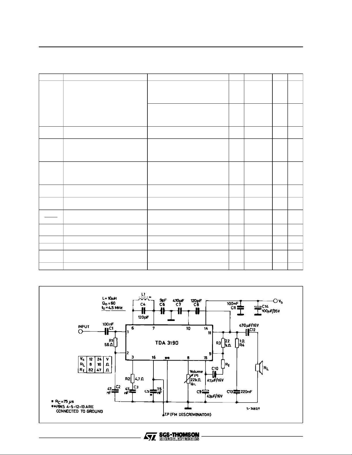
TYPICAL CIRCUIT
3190-03.EPS
3/9

TDA3190
Figure 1 : RelativeAudio Output Voltageand Out-
put Noiseversus Input Signal
Figure 3 : AmplitudeModulationRejection
versus Input Signal
Figure2 : OutputVoltageAttenuationversus
DC Volume ControlResistance
3190-04.EPS
Figure4 : ∆AMR versus TuningFrequency
Change
3190-05.EPS
Figure 5 : RecoveredAudio Voltage versusUn-
loadedQ Factor of theDetectorCoil
4/9
3190-06.EPS
Figure6 : DistortionversusOutput Power
3190-08.EPS
3190-07.EPS
3190-09.EPS

TDA3190
Figure 7 : Distortion versusFrequency
Deviation
Figure 9 : Audio Amplifier FrequencyResponse
Figure8 : DistortionversusTuningFrequency
Change
3190-10.EPS
Figure10 : SupplyVoltageRipple Rejection ver-
sus Ripple Frequency
3190-11.EPS
Figure 11 : Supply VoltageRippleRejection ver-
sus VolumeControl Attenuation
3190-12.EPS
Figure12 : OutputPower versusSupply Voltage
3190-14.EPS
3190-13.EPS
3190-15.EPS
5/9

TDA3190
Figure 13 : MaximumPower Dissipationversus
Supply Voltage (sinewaveoperation)
Figure 15 : QuiescentOutput Voltage (Pin 11)
versus Supply Voltage
Figure14 : PowerDissipation and Efficiencyver-
sus Output Power
3190-16.EPS
3190-17.EPS
6/9
3190-18.EPS

APPLICATIONINFORMATION
The electrical characteristics of the TDA3190 remainalmost constantoverthefrequencyrange 4.5
to 6 MHz, thereforeit can be used in all television
standards (FM mod.). The TDA3190 has a high
inputimpedance,so it canworkwithaceramicfilter
or with a tuned circuit that provide the necessary
input selectivity.
The value of the resistors connected to pin 9,
determinethe AC gainof the audio frequencyamplifier. This enablesthe desiredgain tobe selected
in relation to the frequency deviation at which the
output stage of the AF amplifier, must enter into
Figure 16 : TypicalApplicationCircuit
TDA3190
clipping.
CapacitorC8, connectedbetween pins10 and11,
determinesthe uppercutofffrequencyofthe audio
bandwidth.Toincreasethebandwidththe valuesof
C8 and C7 must be reduced, keeping the ratio
C7/C8 as shown in thetable of fig. 16.
The capacitor connected between pin 16 and
ground,togetherwith theinternalresistorof 10KΩ
forms the de-emphasis network. The Boucherot
cell eliminates the high frequency oscillations
causedbythe inductiveloadandthewiresconnecting theloudspeaker.
Figure 17 : P.C. Board and ComponentLayout of the Circuit shown in Figure 16 (1 :1 scale)
3190-19.EPS
3190-20.TIF
7/9

TDA3190
MOUNTING INSTRUCTION
The Rthj-amb of the TDA3190can be reduced by
soldering the GND pins to a suitablecopper area
ofthe printed circuitboard (fig.18)or toan external
heatsink(fig. 19).
The diagram of figure 20 shows the maximum
dissipablepowerPtotand theRth j-amb asa functionoftheside”l” oftwoequalsquare copperareas
Figure 18 : Exampleof P.C.Board CopperArea
which is used as Heatsink
havinga thicknessof 35 µ (1.4mils).
During soldering the pins temperature must not
exceed 260°C andthe solderingtime must not be
longer than 12 seconds.
The externalheatsinkor printedcircuitcopperarea
must beconnected to electricalground.
Figure19 : ExternalHeatsinkMountingExample
Figure 20 : MaximumDissipablePower andJunc-
tion to AmbientThermal Resistance
versus Side ”T”
3190-21.EPS
Figure21 : MaximumAllowable Power Dissipa-
tionversus AmbientTemperature
3190-23.EPS
3190-22.EPS
3190-24.EPS
8/9

PACKAGE MECHANICAL DATA
16 PINS- PLASTICDIP
TDA3190
I
L
b1
E
Dimensions
a1
Z
b
16
18
Be
e3
D
9
F
Millimeters Inches
Min. Typ. Max. Min. Typ. Max.
a1 0.51 0.020
B 0.77 1.65 0.030 0.065
b 0.5 0.020
b1 0.25 0.010
D 20 0.787
E 8.5 0.335
e 2.54 0.100
e3 17.78 0.700
F 7.1 0.280
i 5.1 0.201
L 3.3 0.130
Z 1.27 0.050
PM-DIP16.EPS
DIP16.TBL
Information furnishedis believed tobe accurate andreliable. However, SGS-THOMSON Microelectronics assumes no responsibility
for the consequences ofuse of such information norfor any infringement ofpatents or other rights of third partieswhich mayresult
from itsuse. Nolicence isgranted by implication orotherwise under any patent or patent rights of SGS-THOMSON Microelectronics.
Specifications mentioned in this publication are subject to change without notice. This publication supersedes and replaces all
information previouslysupplied. SGS-THOMSON Microelectronics productsare not authorized for use ascriticalcomponents in life
support devices or systems without express written approval of SGS-THOMSON Microelectronics.
1994 SGS-THOMSON Microelectronics - All Rights Reserved
Purchase of I
2
I
C Patent. Rights to use these components in a I2C system, isgranted provided that the system conforms to
Australia - Brazil - China - France - Germany- Hong Kong -Italy -Japan - Korea - Malaysia - Malta - Morocco
The Netherlands - Singapore - Spain - Sweden - Switzerland -Taiwan - Thailand- United Kingdom -U.S.A.
2
C Components of SGS-THOMSON Microelectronics, conveys a license under the Philips
2
the I
C Standard Specifications as defined by Philips.
SGS-THOMSON MicroelectronicsGROUP OF COMPANIES
9/9
 Loading...