


.SUPPLYVOLTAGEDOWNTO 3 V
.LOWCROSSOVERDISTORSION
.LOWQUIESCENTCURRENT
.BRIDGEORSTEREOCONFIGURATION
TDA2822
DUALPOWER AMPLIFIER
POWER DIP
(Plastic12+2+2)
DESCRIPTION
The TDA2822 is a monolithic integrated circuit in
12+2+2 powerdip, intended for use as dual audio
poweramplifier inportableradiosandTSsets.
TYPI CAL APP LICATION CIRCUIT (STE RE O)
ORDERING NUMBER : TDA2822
March 1995
1/11

TDA2822
PIN CONNE CTIO N (top view)
SCHEMATI C DIA G RAM
ABSOLUTE MAXIMUM RATINGS
Symbol Parameter Value Unit
Supply Voltage 15 V
V
s
Output Peak Current 1.5 A
I
o
T
2/11
P
tot
stg,Tj
Total Power Dissipation at T
at T
case
=70°C
Storage and Junction Temperature – 40 to 150 °C
amb
=50°C
1.25
4
W
W

TDA 2822
THERMAL DATA
Symbol Parameter Value Unit
R
th j-amb
R
th j-case
Thermal Resistance Junction-ambient
Thermal Resistance Junction-pins
Max
Max
80
20
°C/W
°C/W
ELECTRICAL CHARACTERISTICS (Vs = 6 V, T
=25°C, unless otherwise specified)
amb
STEREO (test circuit of fig. 1)
Symbol Parameter Test Condition Min. Typ. Max. Unit
Supply Voltage 3 15 V
V
s
Quiescent Output Voltage Vs=9V
V
c
Quiescent Drain Current 6 12 mA
I
d
Input Bias Current 100 nA
I
b
Output Power
P
o
(each channel)
Closed Loop Voltage Gain f = 1 kHz 36 39 41 dB
G
v
Input Resistance f = 1 kHz 100 kΩ
R
i
e
N Total Input Noise Rs=10kΩ
=6V
V
s
d = 10 % f = 1 kHz
=9V RL=4Ω
V
s
=6V RL=4Ω
V
s
= 4.5 V RL=4Ω
V
s
1.3
0.45
B = 22 Hz to 22 kHz
Curve A
4
2.7
1.7
0.65
0.32
2.5
2
SVR Supply Voltage Rejection f = 100 Hz 24 30 dB
CS Channel Separation R
=10kΩ f = 1 kHz 50 dB
g
BRIDGE (test circuit of fig. 2)
V
Supply Voltage 3 15 V
s
Quiescent Drain Current RL= ∞ 612mA
I
d
Output Offset Voltage RL=8Ω 10 60 mV
V
os
Input Bias Current 100 nA
I
b
Output Power d = 10 % f = 1 kHz
P
o
d Distortion (f = 1 kHz) R
Closed Loop Voltage Gain f = 1 kHz 39 dB
G
v
Input Resistance f = 1 kHz 100 kΩ
R
i
e
N Total Input Noise Rs=10kΩ
=9V RL=8Ω
V
s
V
=6V RL=8Ω
s
= 4.5 V RL=4Ω
V
s
=8Ω Po= 0.5 W 0.2 %
L
B = 22 Hz to 22 kHz
Curve A
SVR Supply Voltage Rejection f = 100 Hz 40 dB
2.7
0.9
3.2
1.35
1
3
2.5
V
V
W
W
W
µV
µV
W
W
W
µV
µV
3/11

TDA2822
Figure 1 : Test Circuit (stereo).
Figure 2 : P.C. BoardandComponentsLayoutof theCircuitofFigure1 (1:1 scale).
4/11
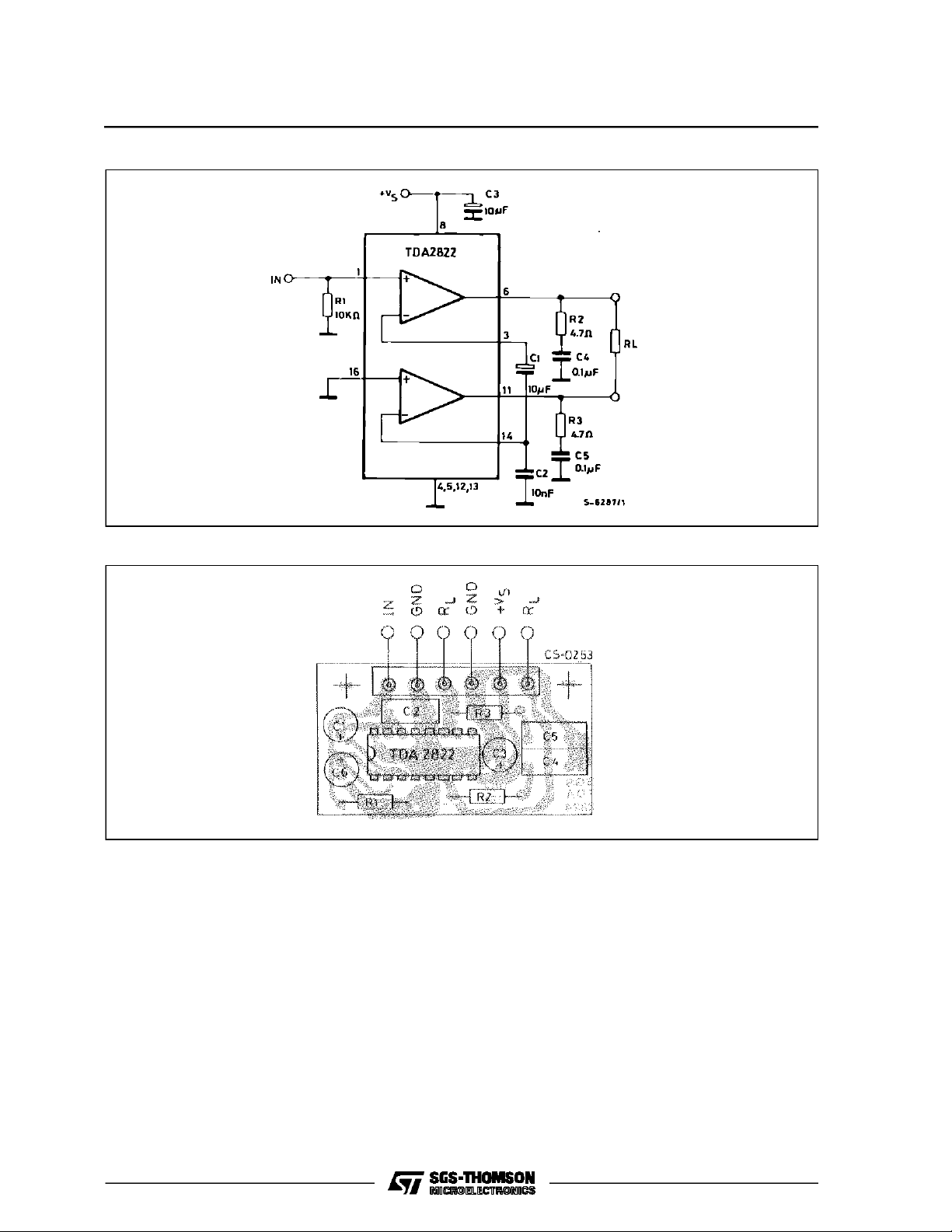
Figure 3 : Test Circuit (bridge).
Figure 4 : P.C. BoardandComponentsLayoutof theCircuitofFigure3 (1:1 scale).
TDA 2822
5/11

TDA2822
Figure 5 : OutputPowervs. SupplyVoltage
(Stereo).
Figure6: OutputPowervs. Supply Voltage
(Bridge).
Figure 7 : Distorsionvs. OutputPower (Bridge). Figure8: Distorsionvs. OutputPower (Bridge).
Figure 9 : SupplyVoltageRejectionvs.
Frequency.
6/11
Figure10 : QuiescentCurrentvs.SupplyVoltage.

TDA 2822
Figure 11 : TotalPowerDissipation vs. Output
Power(Stereo).
Figure 13 : TotalPowerDissipation vs. Output
Power(Bridge).
Figure 12: TotalPowerDissipationvs.Output
Power(Bridge).
7/11
TDA2822
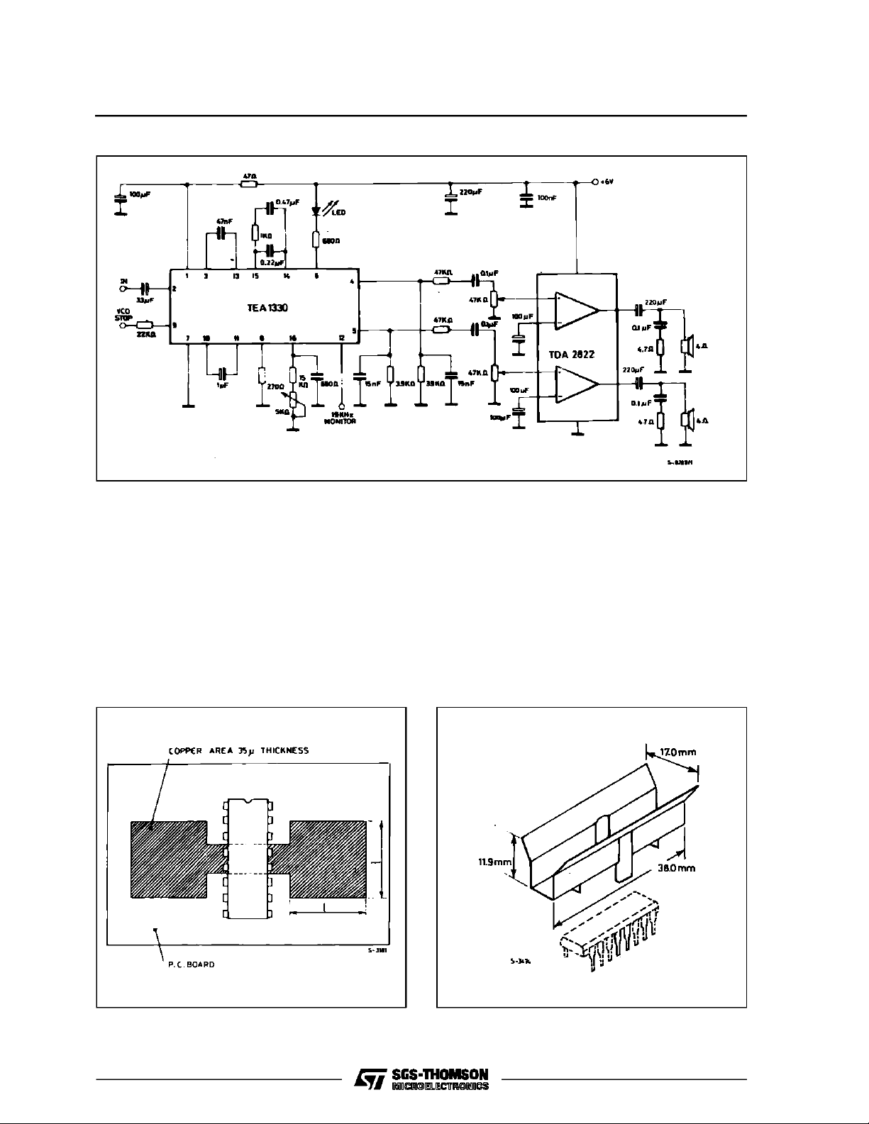
Figure 14 : ApplicationCircuitfor PortableRadios.
MOUNTING I NSTRUCTION
TheR
deringtheGNDpins toa suitablecopperareaof the
printed circuit board (Figure 15) or to an external
heatsink(Figure16).
Thediagram of Figure17showsthemaximum dissipablepowerP
theside”∂” oftwoequalsquarecopperareashaving
a thicknessof 35µ (1.4mils).
oftheTDA2822canbe reducedbysol-
thj-amb
andtheR
tot
as a functionof
th j-amb
Duringsolderingthe pinstemperaturemust notexceed 260 °C and the soldering time must not be
longer than12 seconds.
The externalheatsinkor printedcircuit copperarea
mustbeconnectedto electrical ground.
Figure 15 : Exampleof P.C. BoardCopper Area
which is used asHeatsink.
8/11
Figure16 : ExternalHeatsinkMountingExample.

TDA 2822
Figure 6 : MaximumDissipablePower and
Junctionto AmbientThermal
Resistancevs. Side”∂”.
Figure 7 : MaximumAllowablePower Dissipation
vs. AmbientTemperature.
9/11

TDA2822
POWERDIP16 PACKAGE MECHANICAL DATA
DIM.
MIN. TYP. MAX. MIN. TYP. MAX.
a1 0.51 0.020
B 0.85 1.40 0.033 0.055
b 0.50 0.020
b1 0.38 0.50 0.015 0.020
D 20.0 0.787
E 8.80 0.346
e 2.54 0.100
e3 17.78 0.700
F 7.10 0.280
I 5.10 0.201
L 3.30 0.130
Z 1.27 0.050
mm inch
10/11

TDA 2822
Information furnished is believed to be accurate and reliable. However, SGS-THOMSON Microelectronics assumes no responsibility for
the consequences of use of such information nor for any infringement of patents or other rights of third parties which may result from its
use. No license is granted by implication or otherwise under any patent or patent rights of SGS-THOMSON Microelectronics. Specifications mentioned in this publication are subject to change without notice. This publication supersedes and replaces all information previously supplied. SGS-THOMSON Microelectronics products are not authorized for use as critical components in life support devices or
systems without express writtenapproval of SGS-THOMSON Microelectronics.
1995 SGS-THOMSON Microelectronics - All Rights Reserved
Australia - Brazil - France - Germany - Hong Kong - Italy - Japan - Korea - Malaysia - Malta - Morocco - The Netherlands - Singapore-
SGS-THOMSON Microelectronics GROUP OF COMPANIES
Spain - Sweden - Switzerland - Taiwan - Thaliand - United Kingdom - U.S.A.
11/11
 Loading...