

SGS Thomson Microelectronics TDA2541, TDA2540 Datasheet
IF AMPLIFIERWITHDEMODULATOR AND AFC
.
SUPPLYVOLTAGE: 12V TYP
.
SUPPLYCURRENT : 50mATYP
.
I.F. INPUT VOLTAGE SENSITIVITY AT
PP
RMS
TYP
TYP
F =38.9MHz :85µV
.
VIDEO OUTPUT VOLTAGE (white at 10% of
top synchro): 2.7V
.
I.F. VOLTAGE GAIN CONTROL RANGE :
64dB TYP
.
SIGNAL TO NOISE RATIO AT VI= 10mV :
58dB TYP
.
A.F.C. OUTPUT VOLTAGE SWING FOR
∆f = 100kHz: 10V TYP
DESCRIPTION
The TDA2540and 2541 are IF amplifier and A.M.
demodulatorcircuitsfor colourandblackand white
televisionreceiversusingPNPorNPNtuners.They
are intended for reception of negative or positive
modulationCCIR standard.
They incorporatethe followingfunctions :
.
Gaincontrolled amplifier
.
Synchronousdemodulator
.
Whitespot inverter
.
Video preamplifier with noise protection
.
SwitchableAFC
.
AGCwith noise gating
.
Tuner AGC output (NPN tuner for 2540)-(PNP
tuner for 2541)
.
VCR switch for video output inhibition (VCR
play back)
TDA2540
TDA2541
DIP16
(Plastic Package)
ORDER CODE : TDA2540-TDA2541
PIN CONNECTIONS
DECOUPLINGCAPACITOR
TUNER AGC TAKE-OVERADJUST
TUNERAGC OUTPUT
AFC DEMODULATOR L.C. NETWORK
REFERENCEL.C. NETWORK
August 1992
IF INPUT
AFCOUTPUT
AFC SWITCH
1
2
3
4
5
6
7
8
16
15
14
13
12
11
10
IF INPUT
DECOUPLINGCAPACITOR
AGC CAPACITOR
GROUND
VIDEO OUTPUT
V
CC
AFCDEMODULATORL.C. NETWORK
9
REFERENCEL.C. NETWORK
2540-01.EPS
1/7

TDA2540 - TDA2541
BLOCK DIAGRAM
ABSOLUTE MAXIMUMRATINGS
Symbol Parameter Value Unit
V (11–13) Supply Voltage 13.8 V
V (4–13) Tuner A.G.C. Voltage 12 V
T
P
T
tot
stg
amb
Power Dissipation 900 mW
Storage Temperature – 55 to + 125 °C
Operating Ambient Temperature 0 to + 70 °C
THERMALDATA
Symbol Parameter Value Unit
R
th (j-a)
Junction - ambient Thermal Resistance 70 °C/W
ELECTRICAL OPERATING CHARACTERISTICS
=25oC;V
T
amb
Symbol Parameter Min. Typ. Max. Unit
V
11-13
I
V
11
1-16
Supply Voltage Range 10.2 12 13.8 V
Supply Current 50 60 mA
IF Input Voltage Sensitivity 60 85 180 µV
Max Input Voltage (Pins 1-16) 140 mV
V
V
V
12-13
Z
12-13
12-13
∆G
1-16
Video Output Voltage 2.7 V
Differential Input Impedance (in parallel with 2pF) 2 kΩ
Zero Signal Output Level 5.7 6 6.3 V
Top Synchro Output Level 2.9 3.07 3.2 V
IF Voltage Gain Control Range 52 64 dB
V
=12V; f =38.9MHz (unless otherwise specified)
11–13
2540-02.TIF
2540-01.TBL
2540-02.TBL
RMS
pp
2540-03.TBL
2/7
TDA2540- TDA2541
ELECTRICAL OPERATING CHARACTERISTICS (continued)
=25°C; V (11 – 13) = 12 V; f = 38.9 MHz (unlessotherwise specified)
T
amb
Symbol Parameter Min. Typ. Max. Unit
S/N Signal to Noise Ratio (V
B Bandwidth of Video Amplifier (– 3dB) 6 MHz
dG Differential Gain 4 10 %
dφ Differential Phase 2 10 %
V
V
12-13
12-13
Carrier Signal at Video Output (VI= 10mV) 4 30 mV
2nd Harmonic of Carrier at Video Output (VI= 10mV) 20 30 mV
Intermodulation at 1.1MHz (blue) (see Figures 2 and 3) 46 60 dB
Intermodulation at 1.1MHz (yellow) (see Figures 2 and 3) 46 50 dB
Intermodulation at 3.3MHz (blue) (see Figures 2 and 3) 46 54 dB
V
14-13
VCR Switches Off Output at : (VCR = low Level) 1.1 V
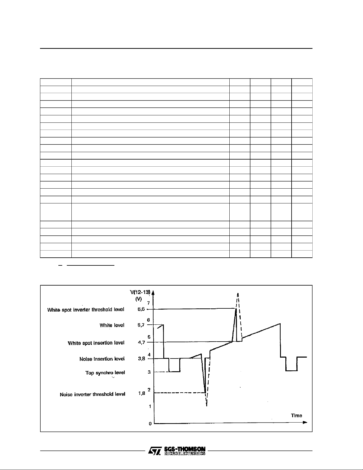
White Spot Inverter Threshold Level (see Figure 1) 6.6 V
White Spot Insertion Level (see Figure 1) 4.7 V
Noise Inverter Threshold Level (see Figure 1) 1.8 V
Noise Insertion Level (see Figure 1) 3.8 V
V
I
4
14-13
I
4
Tuner AGC output Current Range 0 to 10 mA
Tuner AGC Output Voltage 0.3 V
Tuner AGC Output Leakage Current
TDA2541 V
TDA2540 V
∆V
5-13
AFC Output Voltage Swing (∆f = 100 kHz) 10 11 V
∆f Change of Frequency at AFC Output (voltage swing of 10V) 100 200 kHz
V
V
V
Note : 1.
6-13
6-13
5-13
AFC Switches OFF (AFC = low level) at : 2.5 V
AFC Switches LOW (AFC = High level) at : 3.2 V
AFC Zero = Signal Output Voltage (minimum gain) 4 6 8 V
V
S
N
(black to white)
O
=
V
⋅ (RMS at B = 5MHz)
N
= 10mV) (see note 1) 50 58 dB
I
(dB)
14-13
14-13
= 11V, V
= 5V, V
4-13
4-13
= 12V
= 12V
15 µA
RMS
RMS
2540-04.TBL
Figure1 : Video Output Waveform Showing White Spotand Noise Inverter ThresholdLevels
2540-03.TIF
3/7
 Loading...