SGS Thomson Microelectronics TDA2050 Datasheet

32W Hi-Fi AUDIO POWERAMPLIFIER
HIGHOUTPUTPOWER
(50W MUSICPOWERIEC 268.3 RULES)
HIGHOPERATINGSUPPLYVOLTAGE(50V)
SINGLEOR SPLIT SUPPLYOPERATIONS
VERYLOWDISTORTION
SHORT CIRCUIT PROTECTION (OUT TO
GND)
THERMAL SHUTDOWN
TDA2050
Pentawatt
DESCRIPTION
The TDA 2050 is a monolithicintegrated circuit in
Pentawatt package, intended for use as an audio
classAB audio amplifier.Thanksto its high power
capability the TDA2050 is able to provide up to
35W true rms power into 4 ohm load @ THD =
10%, V
8ohmload @THD = 10%, V
= ±18V, f = 1KHz and up to 32W into
S
= ±22V, f = 1KHz.
S
Moreover, the TDA 2050 delivers typically 50W
music power into 4 ohm load over 1 sec at V
S
22.5V,f =1KHz.
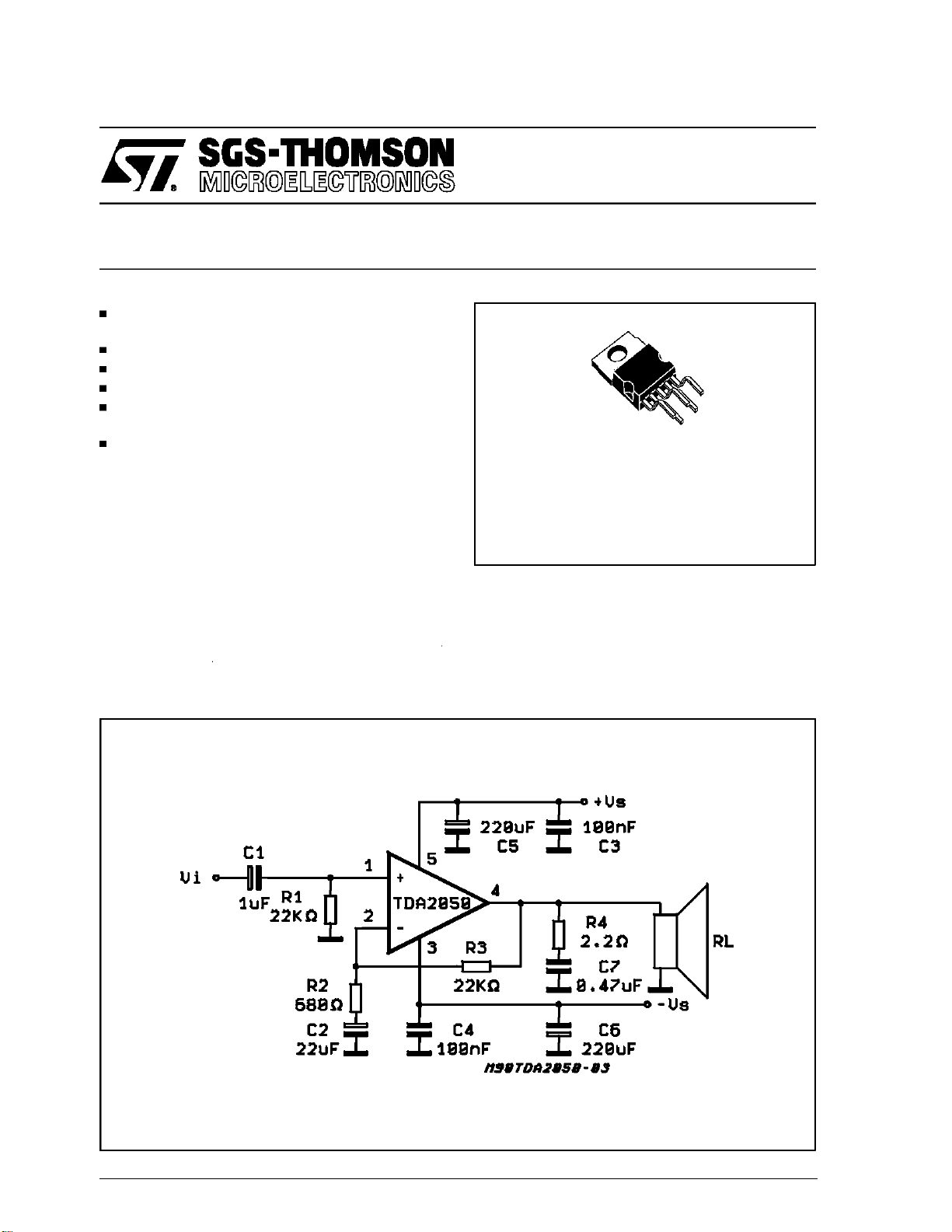
TEST AND APPLICATION CIRCUIT
ORDERING NUMBERS: TDA2050V
TDA2050H
Thehigh power and very low harmonic and crossover distortion (THD = 0.05% typ, @ V
P
= 0.1 to 15W, RL=8ohm, f = 100Hz to 15KHz)
O
make the device most suitable for both HiFi and
=
high class TV sets.
= ±22V,
S
March 1995
This is advanced information on anew product now in development or undergoing evaluation. Details are subject to change withoutnotice.
1/13

TDA2050
ABSOLUTE MAXIMUMRATINGS
Symbol Parameter Value Unit
V
V
V
I
P
T
stg,Tj
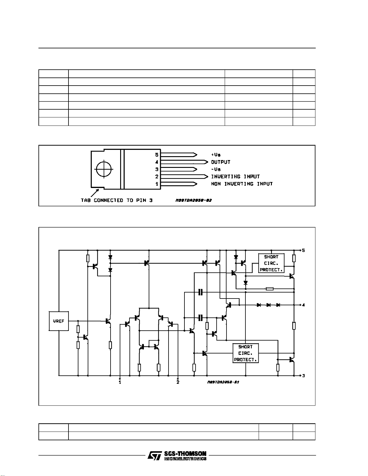
PIN CONNECTION (Top view)
Supply Voltage ±25 V
S
Input Voltage V
i
Differential Input Voltage ±15 V
i
Output Peak Current (internally limited) 5 A
O
Power DissipationT
tot
=75°C25W
CASE
S
Storage and JunctionTemperature -40 to 150 °C
SCHEMATICDIAGRAM
THERMAL DATA
Symbol Description Value Unit
Thermal Resistance junction-case Max 3 °C/W
2/13
R
th j-case

TDA2050
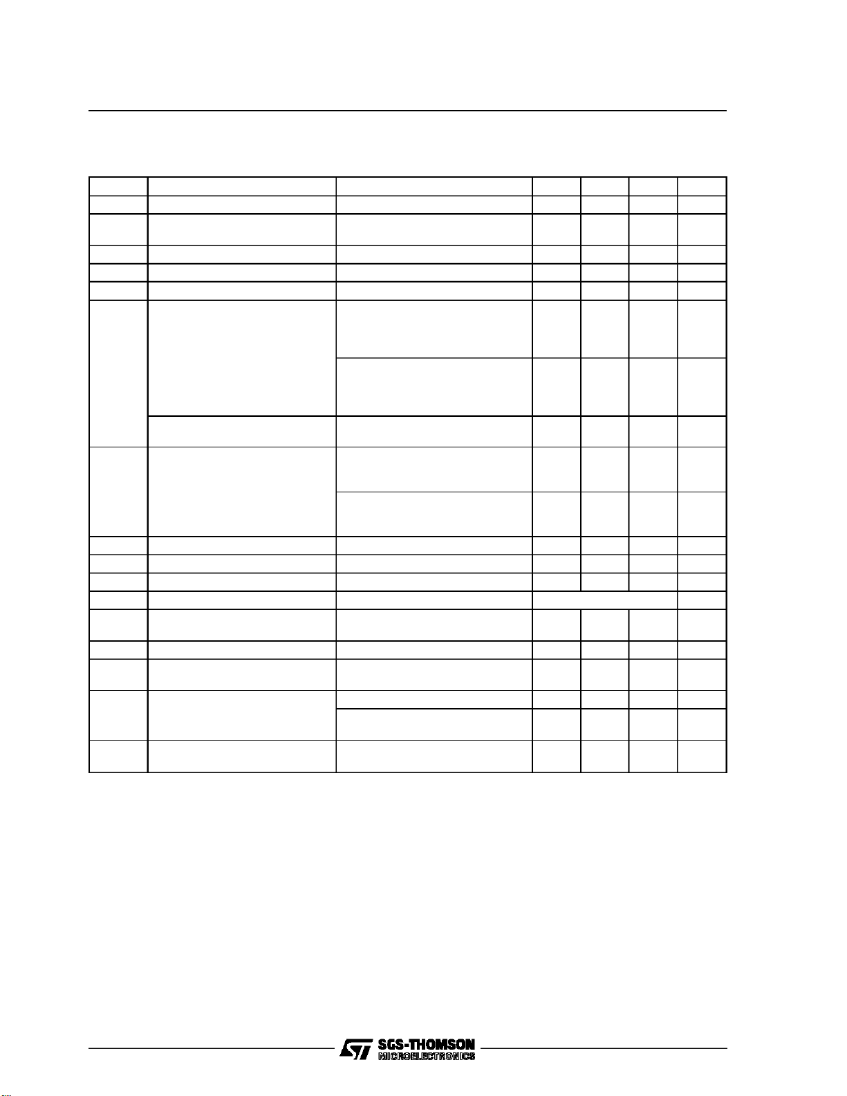
ELECTRICAL CHARACTERISTICS (Refer to the Test Circuit, VS= ±18V, T
=25°C, f = 1 kHz; un-
amb
less otherwisespecified)
Symbol Parameter Test Condition Min. Typ. Max. Unit
V
V
I
OS
P
SR Slew Rate 5 8 V/µs
G
G
BW Power Bandwidth (-3dB) R
e
R
SVR Supply Voltage Rejection R
T
Supply Voltage Range ±4.5 ±25 V
S
Quiescent Drain Current VS= ±4.5V
I
d
Input Bias Current VS= ±22V 0.1 0.5 µA
I
b
Input Offset Voltage VS= ±22V ±15 mV
OS
V
S
= ±25V
30
55
Input Offset Current VS= ±22V ±200 nA
RMS OutputPower d =0.5%
O
R
=4Ω
L
R
=8Ω
L
V
=±22V RL=8Ω
S
24
22
28
18
25
d =10%
R
=4Ω
L
R
=8Ω
L
V
=±22V RL=8Ω
S
Music Power
IEC268.3 RULES
d Total Harmonic Distortion R
Open Loop VoltageGain 80 dB
V
Closed Loop Voltage Gain 30 30.5 31 dB
V
Total Input Noise curve A
N
d =10%; T = 1s
V
= ±22.5V; RL=4Ω 50 W
S
=4Ω
L
f = 1kHz, P
f = 100 Hz to 10kHz, P
= ±22V RL=8Ω
V
S
f = 1kHz, P
f = 100 Hz to 10kHz, P
=4Ω Vi= 200mV 20 to 80,000 Hz
L
= 0.1to 24W
O
= 0.1to 20W
O
= 0.1 to18W
O
= 0.1 to15W
O
B = 22Hz to 22kHz
Input Resistance (pin 1) 500 kΩ
i
= 22kΩ; f = 100Hz;
s
V
= 0.5Vrms 45 dB
ripple
η Efficiency P
Thermal Shut-down
sd-j
= 28W; RL=4Ω 65 %
O
= 25W; RL=8Ω;
P
O
V
=±22V 67 %
S
35
22
32
0.03 0.5
0.02
4
510
150 °C
Junction Temperature
50
90
0.5
0.5
mA
mA
W
W
W
W
W
W
%
%
%
%
µV
µV
3/13

TDA2050
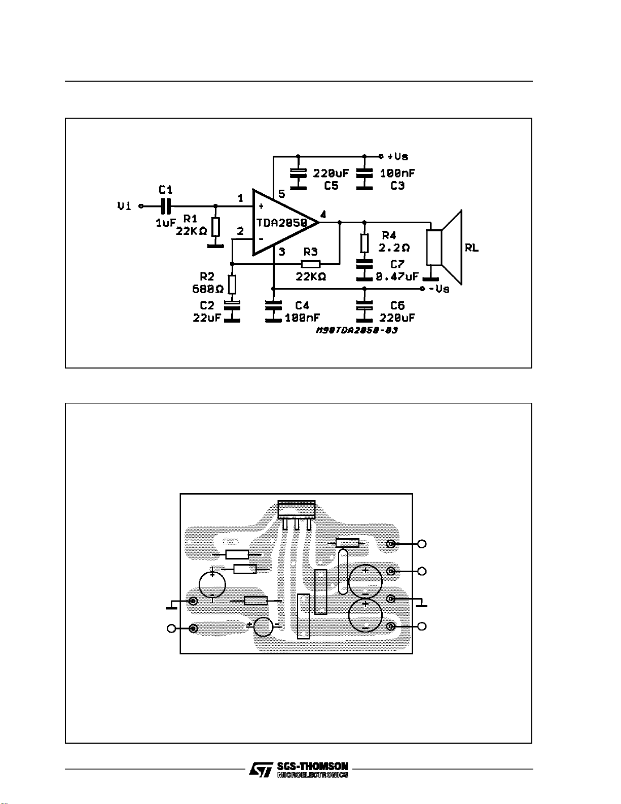
Figure1: Split Supply Typical Application Circuit
Figure2: P.C. Boardand ComponentsLayout of theCircuit of Fig. 1 (1:1)
TDA2050
R4
R3
R2
C2
R1
C4
C1
Vi
C7
C5
C3
C6
R
+Vs
-Vs
L
4/13
 Loading...