

SGS Thomson Microelectronics TDA2040V Datasheet
TDA2040
20W Hi-Fi AUDIOPOWER AMPLIFIER
December 1995
PENTAWATT
ORDERING NUMBER : TDA2040V
DESCRIPTION
The TDA2040 is a monolithicintegrated circuit in
Pentawatt package,intendedforuse asan audio
class ABamplifier.Typicallyit provides22W output
power (d = 0.5%) at V
s
= 32V/4Ω . The TDA2040
provides high output current and has very low
harmonic and cross-over distortion. Further the
deviceincorporatesapatentedshortcircuitprotection system comprising an arrangement for automaticallylimitingthedissipatedpowersoastokeep
the working point of the output transistors within
their safe operating area. A thermal shut-down
system is also included.
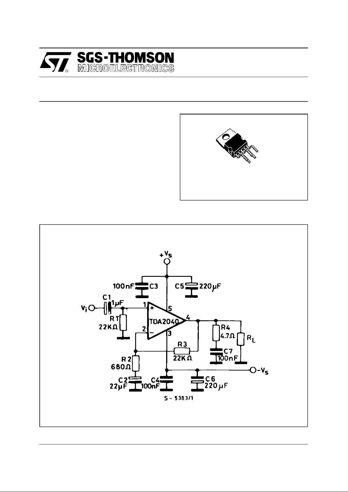
TEST CIRCUIT
1/13

SCHEMATICDIAGRAM
PIN CONNECTION
THERMALDATA
Symbol Parameter Value Unit
R
th j-case
Thermal Resistance Junction-case Max. 3 °C/W
TDA2040
2/13

ELECTRICALCHARACTERISTICS
(refer to the testcircuit, V
S
= ± 16V, T
amb
=25oC unlessotherwise specified)
Symbol Parameter Test Conditions Min. Typ. Max. Unit
V
s
Supply Voltage ± 2.5 ± 20 V
I
d
Quiescent Drain Current Vs= ± 4.5V
V
s
= ± 20V 4530100mAmA
I
b
Input Bias Current Vs= ± 20V 0.3 1 µA
V
os
Input Offset Voltage Vs= ± 20V ± 2 ± 20 mV
I
os
Input Offset Current ± 200 nA
P
o
Output Power d = 0.5%, T
case
=60°C
f = 1kHz R
L
=4Ω
R
L
=8Ω
f = 15kHz R
L
=4Ω
201522
12
18
W
BW Power Bandwidth P
o
= 1W, RL=4Ω 100 kHz
G
v
Open Loop Voltage Gain f = 1kHz 80 dB
G
v
Closed Loop Voltage Gain f = 1kHz 29.5 30 30.5 dB
d Total Harmonic Distortion P
o
= 0.1to 10W, RL=4Ω
f = 40 to 15000Hz
f = 1kHz
0.08
0.03
%
e
N
Input Noise Voltage B = Curve A
B = 22Hz to 22kHz
2
310
µV
µV
i
N
Input Noise Current B = Curve A
B = 22Hz to 22kHz
50
80 200
pA
R
i
Input Resistance (pin 1) 0.5 5 MΩ
SVR Supply Voltage Rejection R
L
=4Ω,Rg= 22kΩ,Gv= 30dB
f = 100Hz, V
ripple
= 0.5V
RMS
40 50 dB
η Efficiency f = 1kHz
P
o
= 12W RL=8Ω
P
o
= 22W RL=4Ω
66
63
%
T
j
Thermal Shut-down JunctionTemperature 145 °C
ABSOLUTEMAXIMUM RATINGS
Symbol Parameter Value Unit
V
s
Supply Voltage ± 20 V
V
i
Input Voltage V
s
V
i
DifferentialInput Voltage ± 15 V
I
o
Output Peak Current (internally limited) 4 A
P
tot
Power Dissipation at T
case
=75°C25W
T
stg,Tj
Storage and Junction Temperature – 40 to + 150 °C
TDA2040
3/13
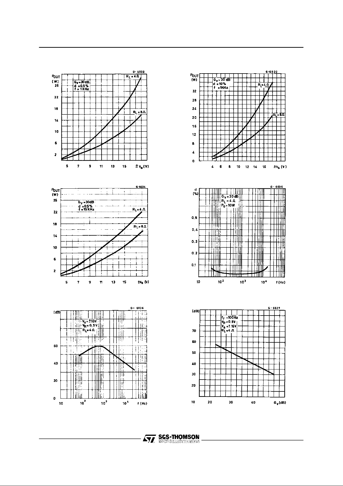
Figure1 : OutputPower versus Supply Voltage Figure 2 : OutputPower versus Supply Voltage
Figure3 : OutputPower versus Supply Voltage Figure 4 : Distortion versus Frequency
Figure5 : Supply Voltage Rejectionversus
Frequency
Figure6 : SupplyVoltage Rejectionversus
VoltageGain
TDA2040
4/13
 Loading...