

.
HIGH OUTPUTPOWER
(10 + 10W Min. @ D = 1%)
.
HIGH CURRENTCAPABILITY(UPTO3.5A)
.
AC SHORTCIRCUITPROTECTION
.
THERMAL OVERLOADPROTECTION
.
SPACE AND COST SAVING : VERY LOW
NUMBER OF EXTERNAL COMPONENTS
AND SIMPLE MOUNTING THANKS TO THE
MULTIWATT
DESCRIPTION
TheTDA2009Ais classABdualHi-Fi Audio power
amplifier assembled in Multiwatt
cially designed for high quality stereo application
asHi-Fi and music centers.
PACKAGE.
package, spe-
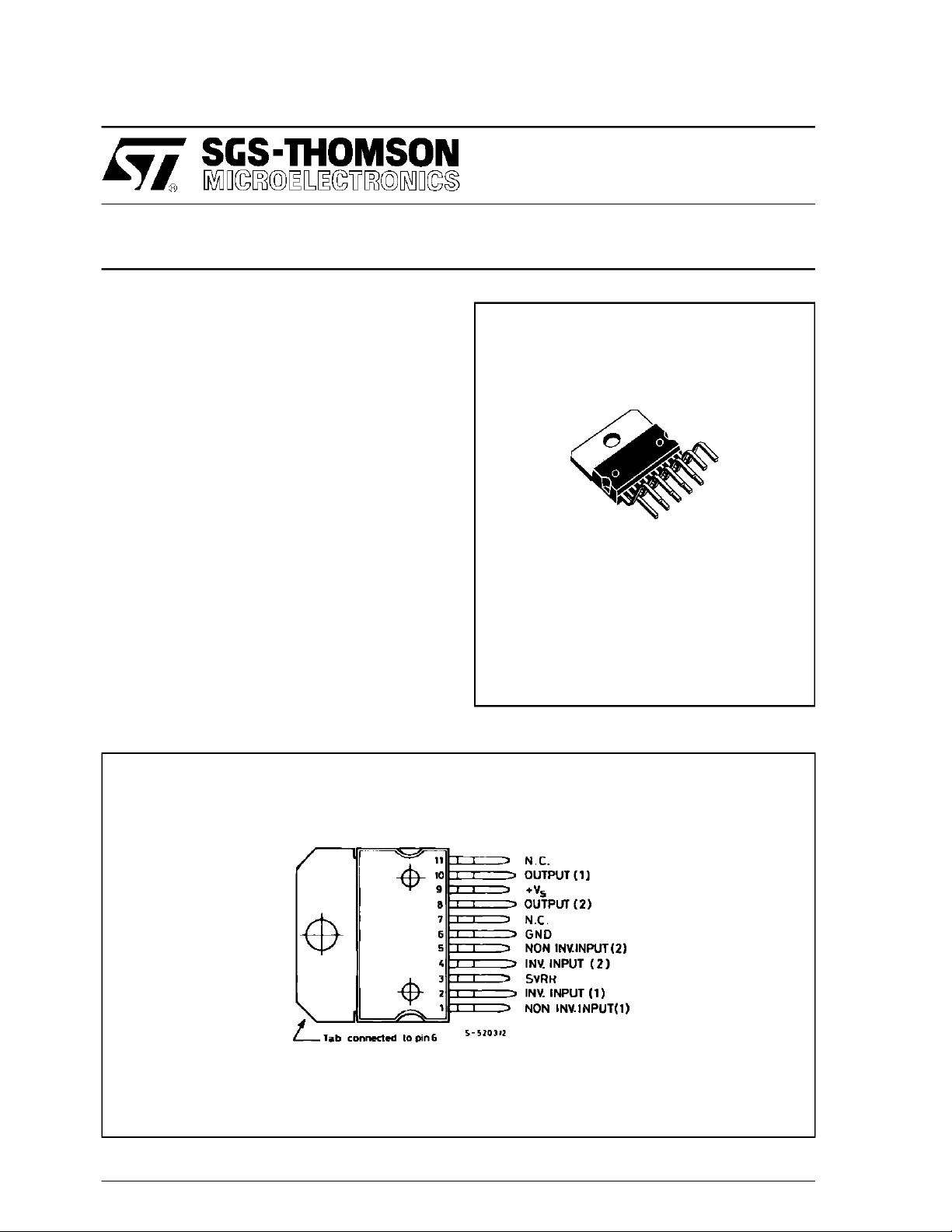
TDA2009A
10 +10W STEREO AMPLIFIER
MULTIWATT11
ORDERING NUMBER : TDA2009A
PIN CONNECTION
May 1995
1/12
TDA2009A
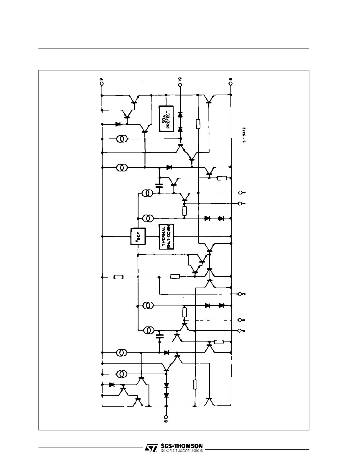
SCHEMATICDIAGRAM
2/12

TDA2009A
ABSOLUTE MAXIMUM RATINGS
Symbol Parameter Value Unit
V
s
I
o
I
o
P
tot
T
stg,Tj
THERMALDATA
Symbol Parameter Value Unit
R
th j-case
ELECTRICALCHARACTERISTICS
(refer to the stereo applicationcircuit,T
Symbol Parameter Test Conditions Min. Typ. Max. Unit
V
s
V
o
I
d
P
o
d Distortion (each channel) f = 1kHz, V
CT Cross Talk (3) R
V
i
R
i
f
L
f
H
G
v
∆G
v
e
N
SVR Supply Voltage Rejection (each channel) R
T
J
Supply Voltage 28 V
Output Peak Current (repetitive f ≥ 20 Hz) 3.5 A
Output Peak Current (non repetitive, t = 100 µs) 4.5 A
Power Dissipation at T
=90°C20W
case
Storage and Junction Temperature – 40, + 150 °C
Thermal Resistance Junction-case Max. 3 °C/W
=25oC, VS= 24V, GV=36dB,unless otherwise specified)
amb
Supply Voltage 8 28 V
Quiescent OutputVoltage Vs= 24V 11.5 V
Total Quiescent Drain Current Vs= 24V 60 120 mA
Output Power (each channel) d = 1%, Vs= 24V, f = 1kHz
=4Ω
R
L
=8Ω
R
L
f = 40Hz to 12.5kHz
=4Ω
R
L
=8Ω
R
L
= 18V, f = 1kHz
V
s
=4Ω
R
L
=8Ω
R
L
= 24V
s
= 0.1 to 7W RL=4Ω
P
o
= 0.1 to 3.5W RL=8Ω
P
o
= 18V
V
s
= 0.1 to 5W RL=4Ω
P
o
= 0.1 to 2.5W RL=8Ω
P
o
= ∞,Rg= 10kΩ
L
f = 1kHz
f = 10kHz
12.5
7
10
5
7
4
0.2
0.1
0.2
0.1
60
50
Input SaturationVoltage (rms) 300 mV
Input Resistance f = 1kHz, Non InvertingInput 70 200 kΩ
Low Frequency Roll off (– 3dB) RL=4Ω 20 Hz
High Frequency Roll off (– 3dB) RL=4Ω 80 kHz
Voltage Gain (closed loop) f = 1kHz 35.5 36 36.5 dB
Closed Loop Gain Matching 0.5 dB
Total Input Noise Voltage Rg= 10kΩ (1)
= 10kΩ (2)
R
g
= 10kΩ
g
= 100Hz, V
f
ripple
ripple
= 0.5V
1.5
2.5 8
55 dB
Thermal Shut-downJunction Temperature 145 °C
W
W
W
W
W
W
%
%
%
%
dB
µV
µV
Notes : 1. Curve A
2. 22Hz to 22kHz
3/12
TDA2009A
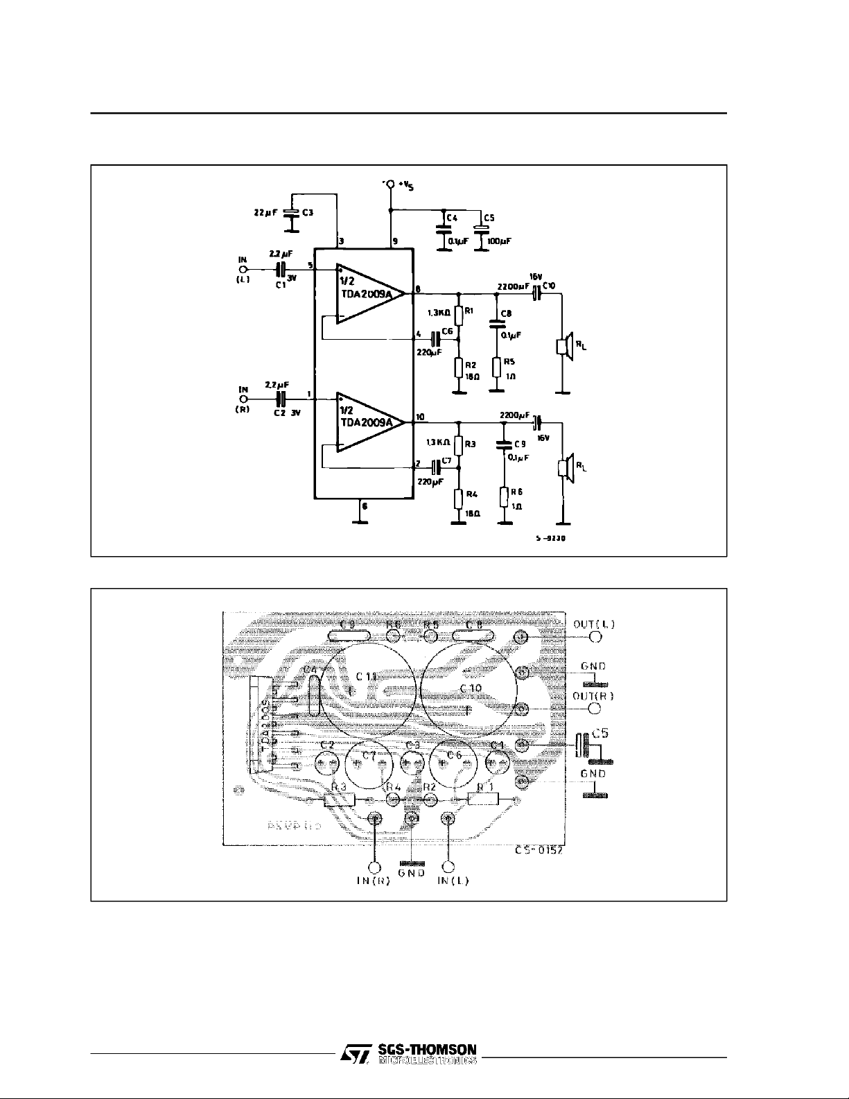
Figure1 : Testand Application Circuit (GV=36dB)
Figure2 : P.C.board and componentlayoutof the fig. 1
4/12

TDA2009A
Figure3 : OutputPowerversusSupply Voltage Figure 4 : Output Power versus SupplyVoltage
Figure5 : Distortion versusOutputPower Figure 6 : Distortionversus Frequency
Figure7 : Distortion versusFrequency Figure 8 : QuiescentCurrent versus
SupplyVoltage
5/12

TDA2009A
Figure9 : SupplyVoltageRejection versus
Frequency
Figure11 : TotalPowerDissipation and
Efficiencyversus Output Power
Figure 10 : Total PowerDissipationand
EfficiencyversusOutputPower
APPLICATION INFORMATION
Figure12 : Example of Muting Circuit
6/12

Figure13 : 10W +10W Stereo Amplifierwith ToneBalanceand Loudness Control
TDA2009A
Figure14 : Tone ControlResponse
(circuit of Figure 13)
7/12

TDA2009A
Figure15 : High Quality20 + 20W TwoWayAmplifier for StereoMusicCenter (one channel only)
Figure16 : 18W Bridge Amplifier(d = 1%, G
=40dB)
V
8/12

TDA2009A
Figure17 : P.C. BOARD and ComponentsLayoutof the Circuitof Figure 16 (1:1 scale)
APPLICATION SUGGESTION
The recommendedvaluesof the componentsare those shown on applicationcircuit of fig. 1. Different
valuescan be used ; the following table can help the designer.
Component
R1, R3 1.2kΩ Close Loop Gain
R2, R4 18kΩ Decrease of Gain Increase of Gain
R5, R6 1Ω Frequency Stability Danger of Oscillation at High
C1, C2 2.2µF Input DC Decoupling High Turn-on Delay High Turn-on Pop.
C3 22µF Ripple Rejection Better SVR. Increase of the
C6, C7 220µF Feedback Input DC
C8, C9 0.1µF Frenquency Stability Danger of Oscillation
C10, C11 1000µFto
(1) The closed loop gain must behigher than 26dB.
Recommended
Value
2200µF
Purpose Larger than Smaller than
Setting (1)
Decoupling
Output DC
Decoupling
Increase of Gain Decrease of Gain
Frequency with Inductive Load
Higher Low Frequency
Cut-off. Increase of Noise
Degradation of SVR
Switch-on Time
Higher Low-frequency
Cut-off
BUILD-IN PROTECTION SYSTEMS
THERMAL SHUT-DOWN
Thepresenceof athermallimiting circuitoffersthe
followingadvantages:
1) an averload on the output (even if it is
pe rman e nt ), o r an e xcessi ve ambien t
temperaturecanbe easilywithstood.
2) the heatsinkcan have a smallerfactor of safety
compared with that of a conventional circuit.
There is no device damage in the case of
excessive junction temperature : all tha t
happensis thatP
(andthereforeP
o
)andIoare
tot
reduced.
The maximum allowable power dissipation depends upon the size of the externalheatsink (i.e.
its thermalresistance); Figure18 shows this dissipable power as a functionofambient temperature
for differentthermal resistance.
Short circuit (AC Conditions). The TDA2009Acan
withstandanaccidentalshortcircuitfromtheoutput
and ground made by a wrong connection during
normal play operation.
9/12

TDA2009A
MOUNTINGINSTRUCTIONS
The power dissipated in the circuit must be removedby adding an external heatsink.
Thanks to the MULTIWATT package attaching
the heatsink is very simple,a screwor a compression spring (clip) being sufficient. Between the
heatsinkandthepackageitisbettertoinsertalayer
of silicon grease, to optimize the thermalcontact;
no electrical isolation is needed between the two
Figure18 : Maximum Allowable Power Dissipa-
tion versusAmbient Temperature
Figure20 : OutputPowerand DrainCurrentver-
susCase Temperature
Figure 19 : Output Power versusCase
Temperature
10/12

MULTIWATT11 PACKAGEMECHANICAL DATA
TDA2009A
DIM.
A 5 0.197
B 2.65 0.104
C 1.6 0.063
D 1 0.039
E 0.49 0.55 0.019 0.022
F 0.88 0.95 0.035 0.037
G 1.45 1.7 1.95 0.057 0.067 0.077
G1 16.75 17 17.25 0.659 0.669 0.679
H1 19.6 0.772
H2 20.2 0.795
L 21.9 22.2 22.5 0.862 0.874 0.886
L1 21.7 22.1 22.5 0.854 0.87 0.886
L2 17.4 18.1 0.685 0.713
L3 17.25 17.5 17.75 0.679 0.689 0.699
L4 10.3 10.7 10.9 0.406 0.421 0.429
L7 2.65 2.9 0.104 0.114
M 4.25 4.55 4.85 0.167 0.179 0.191
M1 4.73 5.08 5.43 0.186 0.200 0.214
S 1.9 2.6 0.075 0.102
S1 1.9 2.6 0.075 0.102
Dia1 3.65 3.85 0.144 0.152
MIN. TYP. MAX. MIN. TYP. MAX.
mm inch
11/12

TDA2009A
Information furnished is believed to be accurate and reliable. However, SGS-THOMSON Microelectronics assumes no responsibility for the
consequences of use of such information nor for any infringement of patents or other rights of thirdparties which may result from its use. No
license is granted by implicationor otherwise underany patentor patentrights of SGS-THOMSON Microelectronics. Specifications mentioned
in this publication are subject to change without notice. This publication supersedes and replaces all information previously supplied.
SGS-THOMSON Microelectronics products arenot authorized for useas critical components inlife supportdevices or systems withoutexpress
written approval of SGS-THOMSON Microelectronics.
1994 SGS-THOMSON Microelectronics - All Rights Reserved
Australia - Brazil -France - Germany - HongKong - Italy - Japan - Korea - Malaysia- Malta- Morocco - TheNetherlands - Singapore -
SGS-THOMSON Microelectronics GROUP OF COMPANIES
Spain - Sweden - Switzerland -Taiwan - Thaliand -United Kingdom - U.S.A.
12/12
 Loading...