


DatasheetArchive.com
Request For Quotation
Order the parts you need from our real-time inventory database.
Simply complete a request for quotation form with your part
information and a sales representative will respond to you with
price and availability.
Request For Quotation
Your free datasheet starts on the next page.
More datasheets and data books are available from our
homepage: http://www.datasheetarchive.com
This datasheet has been downloaded from http://www.datasheetarchive.com.
20W BRIDGE AMPLIFIER FORCAR RADIO
High output power : PO= 10 + 10 W@RL=2Ω,
d = 10% ; P
High reliabilityofthe chipandpackagewith additional complete safety during operation thanks to
protectionagainst:
.
OUTPUT DC AND AC SHORT CIRCUIT TO
GROUND
.
OVERRATINGCHIP TEMPERATURE
.
LOADDUMP VOLTAGESURGE
.
FORTUITOUS OPEN GROUND
.
VERYINDUCTIVE LOADS
Flexibilityin use: bridge or stereo boosteramplifierswithor withoutboostrapand withprogrammable gain and bandwidth.
Space and cost saving : very low number of
external components, very simple mounting system with no electrical isolation between the package and the heatsink(one screwonly).
In addition, the circuitoffersloudspeakerprotec-
tion during short circuit for one wire to ground.
= 20W@RL=4Ω,d=1%.
O
TDA2005
MULTIWATT11
ORDERING NUMBERS : TDA2005M (Bridge Appl.)
TDA2005S (Stereo Appl.)
DESCRIPTION
TheTDA2005is classB dual audiopoweramplifier
in MULTIWATT packagespecificallydesignedfor
car radio application : power booster amplifiers
are easilydesignedusingthis device thatprovides
a high currentcapability (upto 3.5A) and that can
drive very low impedance loads (down to 1.6Ω in
stereo applications) obtaining an output power of
more than 20 W (bridge configuration).
ABSOLUTE MAXIMUMRATINGS
Symbol Parameter Value Unit
V
s
V
s
V
s
(*) Output Peak Current (non repetitive t = 0.1 ms) 4.5 A
I
o
(*) Output Peak Current (repetitive f ≥ 10 Hz) 3.5 A
I
o
P
tot
T
stg,Tj
(*) The max. output current is internally limited.
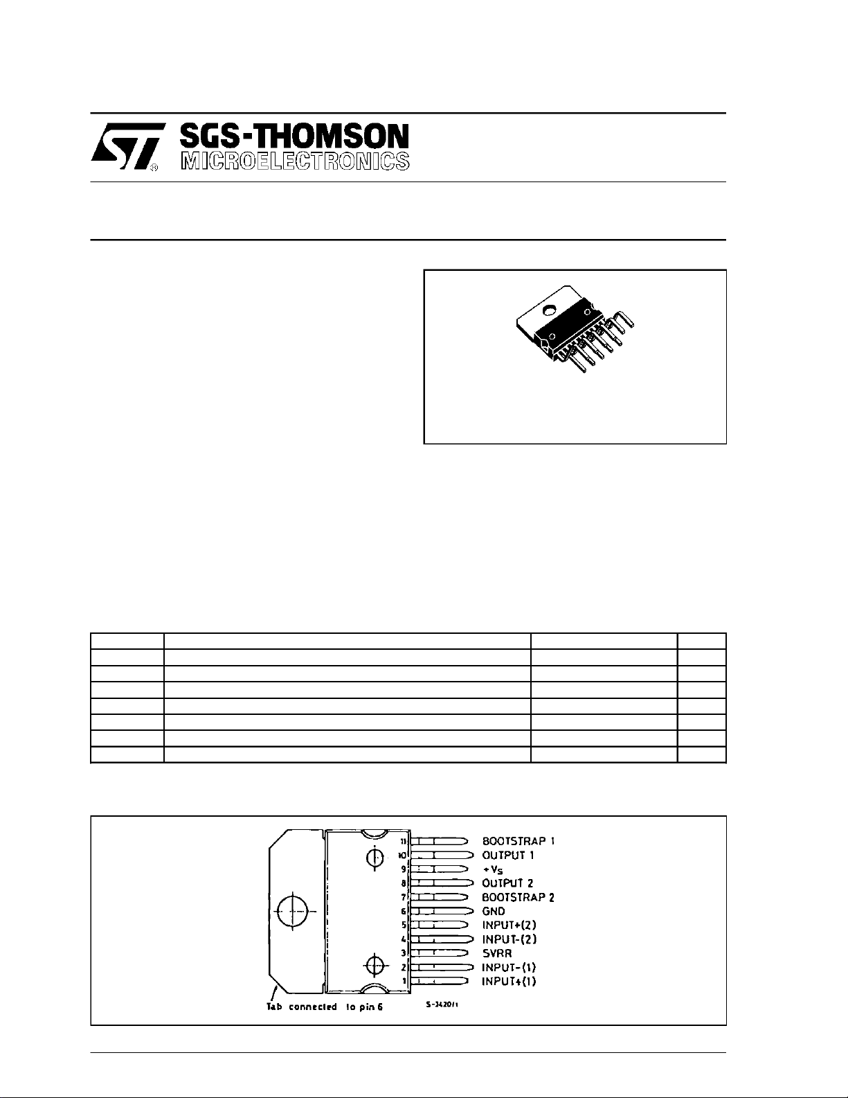
PIN CONNECTION
Operating Supply Voltage 18 V
DC Supply Voltage 28 V
Peak Supply Voltage (for 50 ms) 40 V
Power Dissipation atT
Storage and JunctionTemperature – 40 to 150 °C
=60°C30W
case
March 1995
1/21
TDA2005
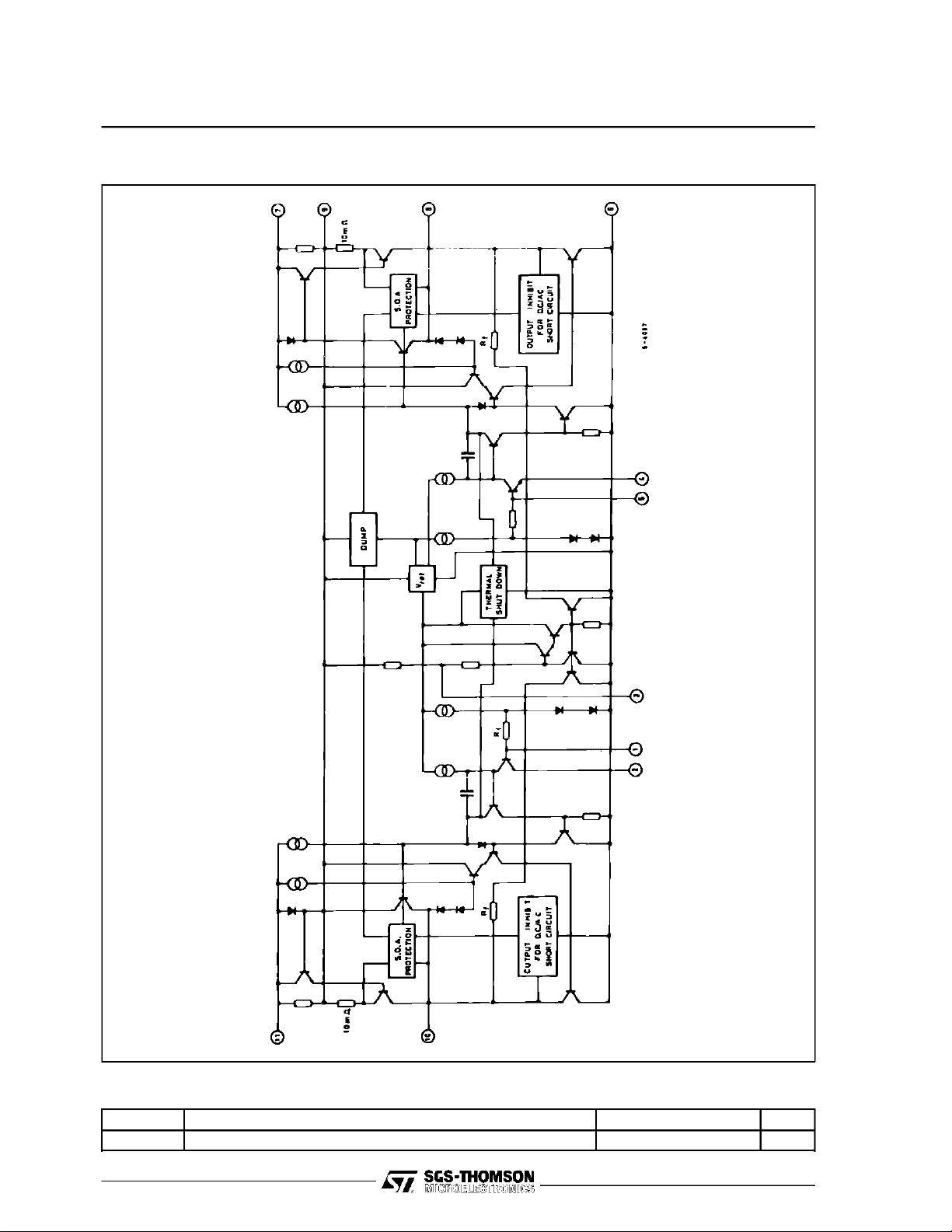
SCHEMATIC DIAGRAM
THERMALDATA
Symbol Parameter Value Unit
Thermal Resistance Junction-case Max. 3 °C/W
2/21
R
th j-case
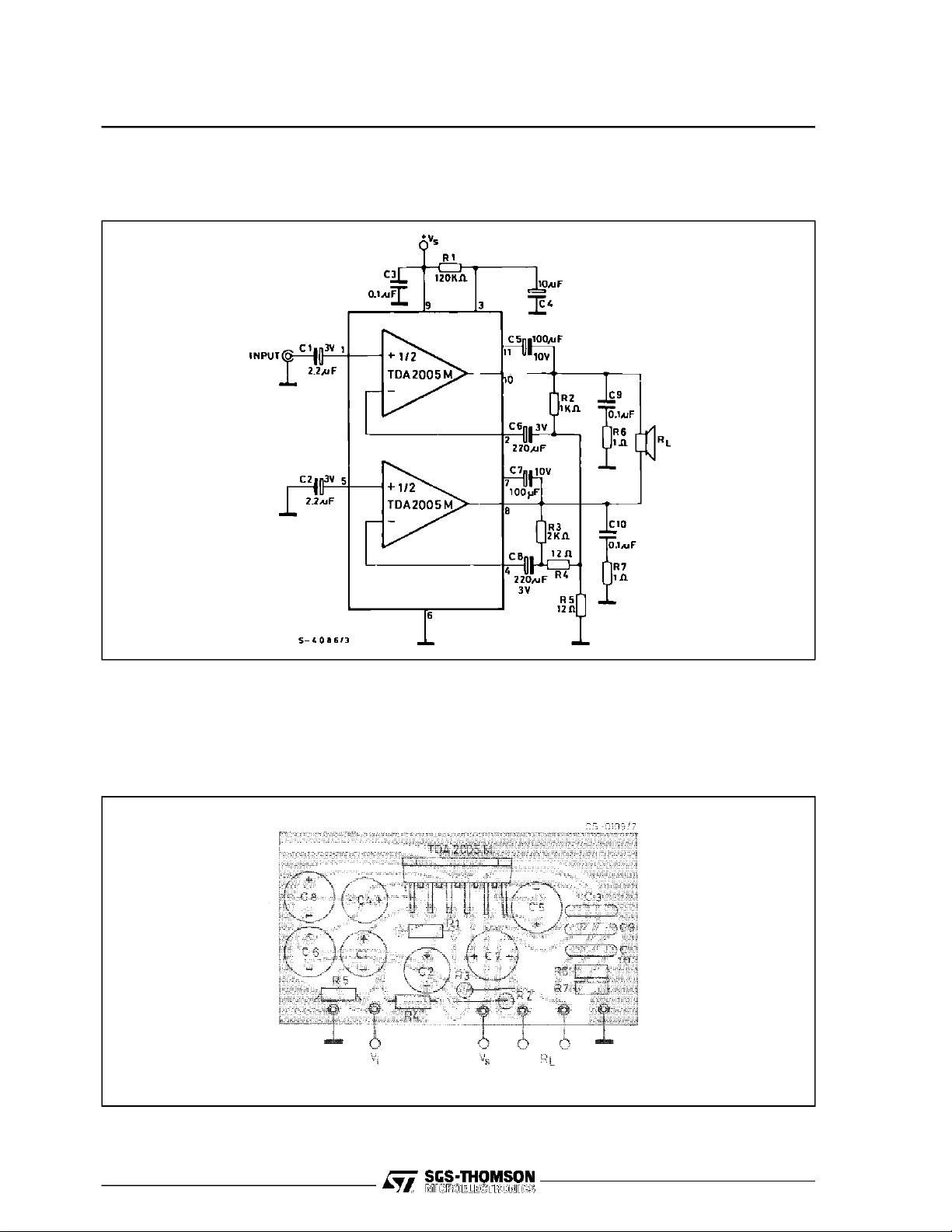
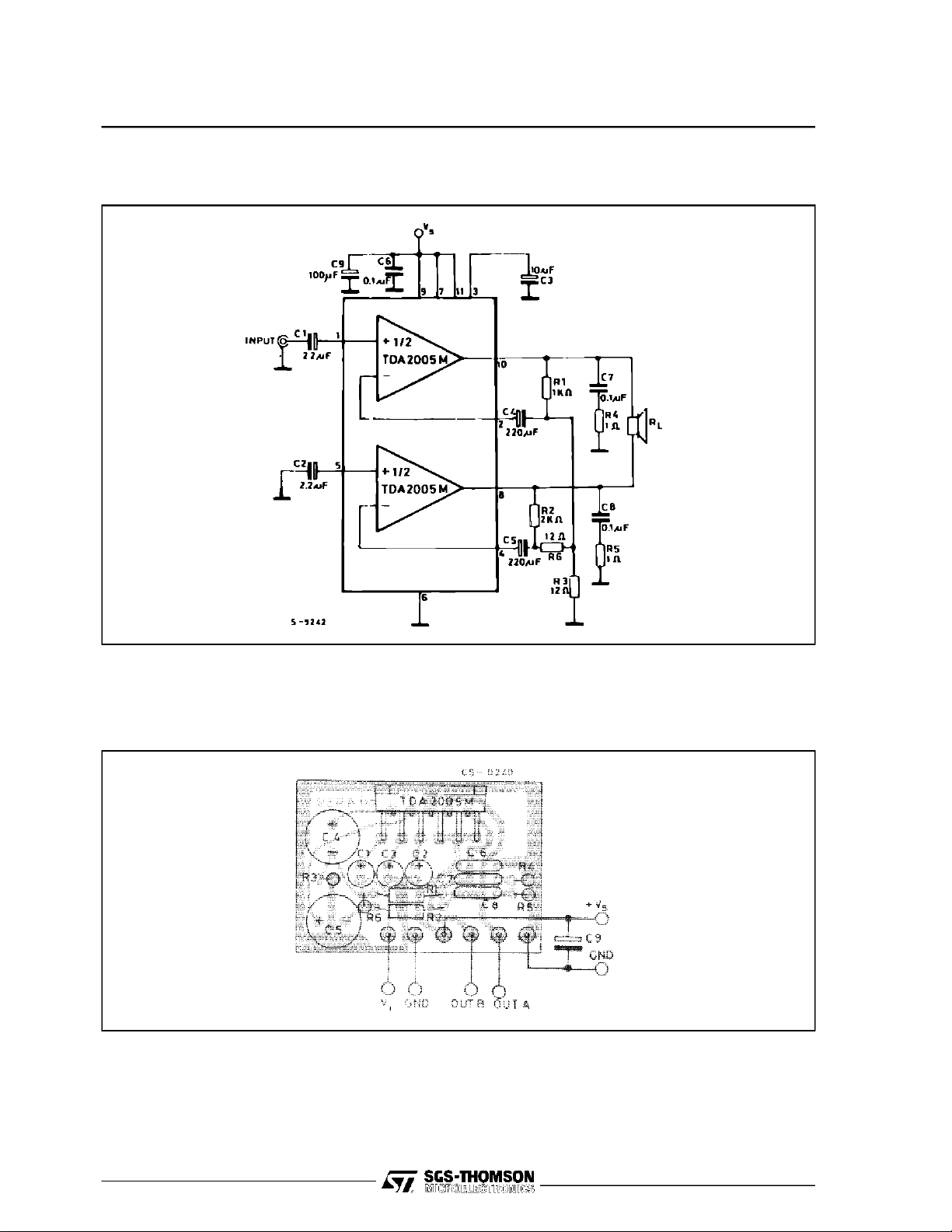
BRIDGE AMPLIFIER APPLICATION(TDA2005M)
Figure1 : Test and ApplicationCircuit (Bridgeamplifier)
TDA2005
Figure2 : P.C.Board and ComponentsLayout of Figure1 (1:1 scale)
3/21

TDA2005
ELECTRICAL CHARACTERISTICS (referto the Bridge applicationcircuit, T
R
th (heatsink
)=4oC/W, unless otherwise specified)
=25oC, GV=50dB,
amb
Symbol Parameter Test Conditions Min. Typ. Max. Unit
V
V
P
Supply Voltage 8 18 V
s
Output Offset Voltage (1)
os
(between pin 8 and pin 10)
Total Quiescent Drain Current Vs= 14.4V RL=4Ω
I
d
Output Power d= 10% f = 1 Hz
o
Vs= 14.4V
= 13.2V
V
s
= 13.2V RL= 3.2Ω
V
s
= 14.4V RL=4Ω
V
s
= 13.2V RL= 3.2 Ω
V
s
R
L
= 3.2Ω
18
20
17
150
150mVmV
7570150
160mAmA
20
22
19
d Distortion f = 1kHz
= 14.4V RL=4Ω
V
s
Input Sensitivity f = 1kHz
V
i
R
f
G
e
Input Resistance f = 1kHz 70 kΩ
i
Low Frequency Roll Off (– 3dB) RL= 3.2Ω 40 Hz
f
L
High Frequency Roll Off (– 3dB) RL= 3.2Ω 20 kHz
H
Closed Loop Voltage Gain f = 1kHz 50 dB
v
Total Input Noise Voltage Rg= 10kΩ (2) 3 10 µV
N
SVR Supply Voltage Rejection R
η Efficiency V
Thermal Shut-down Junction
T
j
Temperature
V
OSH
Notes : 1. For TDA2005M only
Output Voltage with one Side of
the Speaker shorted to ground
2. BandwithFilter : 22Hz to22kHz.
= 50mW to 15W
P
o
= 13.2V RL= 3.2Ω
V
s
= 50mW to 13W
P
o
=2W RL=4Ω
P
o
=2W RL= 3.2Ω
P
o
= 10kΩ,C4=10µF
g
= 100Hz, V
f
ripple
= 14.4V, f = 1 kHz
s
= 20W RL=4Ω
P
o
= 22W RL= 3.2Ω
P
o
= 13.2V, f = 1 kHz
V
s
= 19W RL= 3.2Ω
P
o
ripple
Vs= 14.4V, RL=4Ω
f = 1kHz, P
tot
= 13W
= 0.5V
45 55 dB
60
60
58
145 °C
Vs= 14.4V RL=4Ω
= 13.2V RL= 3.2Ω 2V
V
s
1
1
9
8
W
%
%
mV
mV
%
%
%
4/21
TDA2005
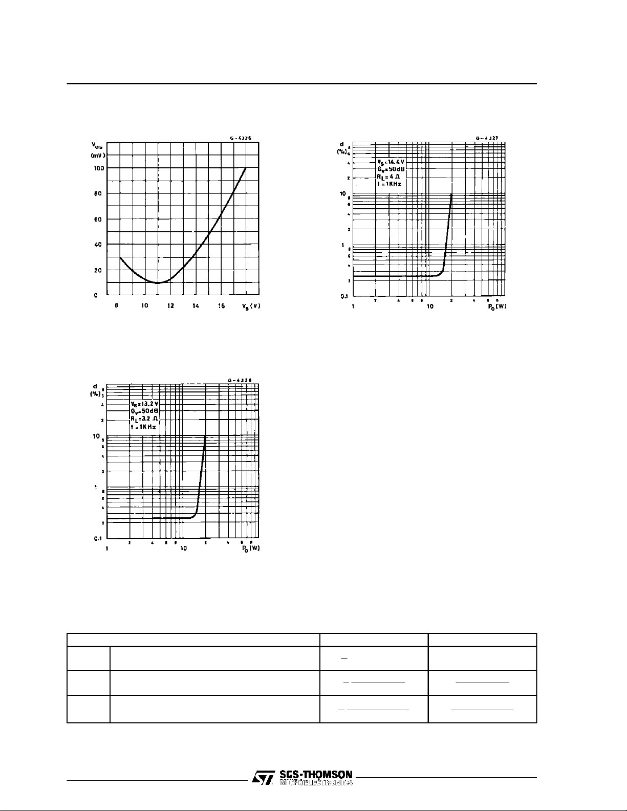
Figure3 : OutputOffset Voltage versus
Supply Voltage
Figure5 : Distortion versus Output Power
(bridge amplifier)
Figure 4 : Distortionversus OutputPower
(bridgeamplifier)
BRIDGEAMPLIFIER DESIGN
The followingconsideraionscan be useful when designing a bridge amplifier.
Parameter Single Ended Bridge
V
o max
I
o max
P
o max
Where : V
Peak Output Voltage (before clipping)
Peak Output Current (before clippling)
RMS OutputPower (before clipping)
= output transistors saturation voltage
CE sat
= allowable supply voltage
V
S
R
= load impedance
L
1
(Vs–2V
2
V
1
S
2
(VS− 2V
1
4
− 2V
R
L
2R
CE sat
CE sat
CE sat
L
)V
2
)
–2V
s
V
− 2V
S
(V
−2V
S
R
2R
CE sat
CE sat
L
CE sat
L
2
)
5/21
TDA2005
Voltageand current swings are twice for a bridge
amplifierincomparisonwithsingleendedamplifier.
In order words, with the same R
the bridge con-
L
figurationcan deliver an output power that is four
timesthe output powerof a singleendedamplifier,
while,with the samemax output current the bridge
configuration can deliver an output power that is
twicethe output power of a singleended amplifier.
Core must be taken when selecting V
and RLin
S
order to avoid an output peak current above the
absolutemaximum rating.
From the expression for I
V
= 14.4V and V
S
= 2V,the minimum load
CE sat
, assuming
O max
that can be driven by TDA2005 in bridge configurationis :
R
L min
V
S
=
I
Omax
CEsat
14.4 −
=
3.5
4
=2.97Ω
− 2V
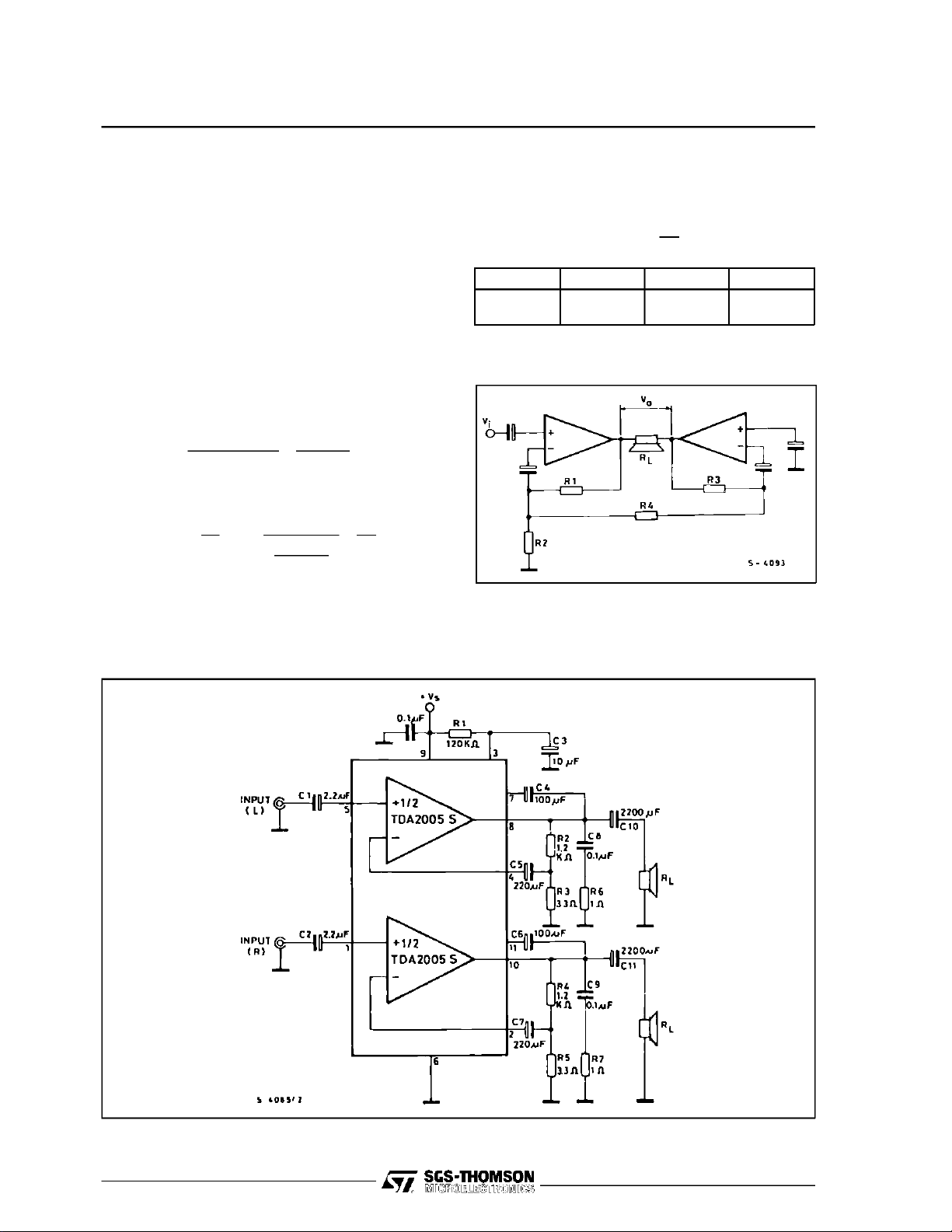
Thevoltagegainofthebridgeconfigurationis given
by(see Figure34) :
V
0
=
V
=1+
1
G
V
R
R
2
R
1
2⋅R4
+R
R
3
+
R
4
4
STEREOAMPLIFIER APPLICATION (TDA2005S)
Forsufficientlyhighgains(40 to 50dB)itis possible
to putR
andR3=2R1, simplifing the formula
2=R4
in :
R
1
=4
G
V
R
2
Gv(dB) R1(Ω)R2=R4(Ω)R3(Ω)
40
50
1000
1000
39
12
2000
2000
Figure6 : Bridge Configuration
Figure7 : TypicalApplicationCircuit
6/21

TDA2005
ELECTRICAL CHARACTERISTICS (referto the Stereo applicationcircuit, T
R
th (heatsink)
=4oC/W, unless otherwwise specified)
=25oC, GV=50dB,
amb
Symbol Parameter Test Conditions Min. Typ. Max. Unit
V
V
P
Supply Voltage 8 18 V
s
Quiescent Output Voltage Vs= 14.4V
o
Total Quiescent Drain Current Vs= 14.4V
I
d
Output Power (each channel) f = 1kHz, d = 10%
o
V
V
V
V
V
= 13.2V
s
= 13.2V
s
= 14.4V RL=4Ω
s
= 13.2V RL= 3.2Ω
s
= 16V RL=2Ω
s
R
R
R
R
L
L
L
L
= 3.2Ω
=2Ω
= 1.6Ω
= 1.6Ω
6.667.2
6
7
9
10
6
9
7.8
6.6
7.2VV
6562120
120mAmA
6.5
8
10
11
6.5
10
12
d Distortion (each channel) f = 1kHz
= 14.4V RL=4Ω
V
CT Cross Talk (1) V
V
V
R
f
G
G
∆ G
e
Input Saturation Voltage 300 mV
i
Input Sensitivity f = 1kHz, Po=1W
i
Input Resistance f = 1kHz 70 200 kΩ
i
Low Frequency Roll Off (– 3dB) RL=2Ω 50 Hz
f
L
High Frequency Roll Off (– 3dB) RL=2Ω 15 kHz
H
Voltage Gain (open loop) f = 1kHz 90 dB
v
Voltage Gain (closed loop) f = 1kHz 48 50 51 dB
v
Closed Loop Gain Matching 0.5 dB
v
Total Input Noise Voltage Rg= 10kΩ (2) 1.5 5 µV
N
SVR Supply Voltage Rejection R
η Efficiency V
Thermal Shut-down JunctionTemperature 145 °C
T
j
Notes : 1. For TDA2005M only
2. Bandwith Filter : 22Hz to 22kHz.
s
= 50mW to 4W
P
o
= 14.4V RL=2Ω
V
s
= 50mW to 6W
P
o
= 13.2V RL= 3.2Ω
V
s
= 50mW to 3W
P
o
= 13.2V RL= 1.6Ω
V
s
= 40mW to 6W
P
o
= 14.4V, Vo=4V
s
RL=4Ω,Rg=5kΩ
f = 1kHz
f = 10kHz
R
L
R
L
= 10kΩ,C3=10µF
g
= 100Hz, V
f
ripple
= 14.4V, f = 1kHz
s
= 6.5W RL=4Ω
P
o
= 10W RL=2Ω
P
o
= 13.2V, f = 1kHz
V
s
= 6.5W RL= 3.2Ω
P
o
= 100W RL= 1.6Ω
P
o
ripple
RMS
=4Ω
= 3.2Ω
= 0.5V
0.2
0.3
0.2
0.3
60
45
5.5
35 45 dB
70
60
70
60
1
1
1
1
6
W
%
%
%
%
dB
mV
%
%
%
%
7/21

TDA2005
Figure8 : Quiescent OutputVoltage versus
Supply Voltage (Stereo amplifier)
Figure10 : Distortionversus Output Power
(Stereo amplifier)
Figure 9 : QuiescentDrain Currentversus
SupplyVoltage (Stereo amplifier)
Figure11 : OutputPower versus Supply Voltage
(Stereoamplifier)
Figure12 : Output Powerversus Supply Voltage
(Stereo amplifier)
8/21
Figure13 : Distortionversus Frequency
(Stereoamplifier)

TDA2005
Figure14 : Distortionversus Frequency
(Stereo amplifier)
Figure16 : Supply Voltage Rejection versus
Frequency(Stereo amplifier)
Figure15 : SupplyVoltage Rejection versus C3
(Stereoamplifier)
Figure17 : SupplyVoltage Rejection versus
C2 andC3 (Stereoamplifier)
Figure18 : Supply Voltage Rejection versus
C2 and C3 (Stereo amplifier)
Figure19 : Gainversus Input Sensitivity
(Stereoamplifier)
9/21

TDA2005
Figure20 : Gain versusInput Sensitivity
(Stereo amplifier)
Figure22 : Total Power Dissipation and Effi-
ciency versus Output Power
(Stereo amplifier)
Figure21 : TotalPower Dissipation andEffi-
ciencyversus Output Power
(Bridgeamplifier)
10/21

TDA2005
APPLICATIONSUGGESTION
The recommendedvalues of the componentsare thoseshown on Bridgeapplicatiioncircuitof Figure 1.
Differentvalues can be used ; the following table can help the designer.
Comp.
R
1
R
2
R
3
R
4,R5
R
6,R7
C
1
C
2
C
3
C
4
C
5,C7
C
6,C8
C
9,C10
Recom.
Value
120 kΩ Optimization ofthe Output
Symmetry
Purpose Larger Than Smaller Than
Smaller P
o max
SmallerP
o max
1kΩ
2kΩ
12 Ω Closed Loop Gain Setting (see
Bridge Amplifier Design) (*)
1Ω FrequencyStability Danger of Oscillation at High
Frequency with Inductive Loads
2.2 µF Input DC Decoupling
2.2 µF Optimization of Turn on Pop and
Turn on Delay
High Turn on Delay Higher Turn on Pop, Higher
Low Frequency Cut-off,
Increase of Noise
0.1 µF Supply by Pass Danger of Oscillation
10 µF Ripple Rejection Increase of SVR, Increase of
Degradation of SVR.
the Switch-on Time
100 µF Bootstrapping Increase of Distortion
at low Frequency
220 µF Feedback Input DC Decoupling,
Low Frequency Cut-off
Higher Low Frequency
Cut-off
0.1 µF Frequency Stability Danger of Oscillation
(*) The closed loop gain must be higher than 32dB.
11/21
TDA2005
APPLICATION INFORMATION
Figure23 : BridgeAmplifierwithout Boostrap
Figure24 : P.C.Board and Components Layout of Figure 23 (1:1 scale)
12/21

APPLICATION INFORMATION(continued)
Figure25 : Dual- Bridge Amplifier
TDA2005
Figure26 : P.C.Board and Components Layout of Figure 25 (1:1 scale)
13/21

TDA2005
APPLICATION INFORMATION(continued)
Figure27 : Low Cost BridgeAmplifier (GV=42dB)
Figure28 : P.C.Board and Components Layout of Figure 27 (1:1 scale)
14/21

APPLICATION INFORMATION(continued)
Figure29 : 10 + 10 W Stereo Amplifier with Tone Balanceand LoudnessControl
TDA2005
Figure30 : Tone Control Response
(circuit of Figure 29)
15/21

TDA2005
APPLICATION INFORMATION(continued)
Figure31 : 20WBus Amplifier
Figure32 : Simple20W TwoWay Amplifier (F
=2kHz)
C
16/21

APPLICATION INFORMATION(continued)
Figure 33 : BridgeAmplifierCircuit suited for Low-gainApplications(GV=34dB)
TDA2005
Figure34 : Exampleof Muting Circuit
17/21

TDA2005
BUILT-IN PROTECTIONSYSTEMS
Load Dump Voltage Surge
The TDA2005 has a circuit which enables it to
withstandavoltagepulsetrain, on Pin9,ofthetype
shown in Figure 36.
If the supply voltage peaks to more than 40V, then
an LC filter must be inserted between the supply
and pin 9, in order to assure that the pulses at pin
9 will be held withing the limits shown.
A suggested LC network is shown in Figure 35.
With this network, a train of pulses with amplitude
upto120Vandwidthof2mscanbeappliedatpoint
A. This type of protection is ON when the supply
voltage(pulse orDC) exceeds18V.Forthisreason
the maximum operating supply voltage is 18V.
Figure35
Figure36
Open Ground
When the ratio is in the ON condition and the
ground is accidentally opened, a standard audio
amplifier will be damaged. On the TDA2005 protectiondiodes are includedto avoid any damage.
Inductive Load
A protection diode is provided to allow use of the
TDA2005 with inductive loads.
DC Voltage
The maximum operating DC voltage for the
TDA2005is 18V.
Howeverthedevice canwithstanda DC voltageup
to 28V with no damage. This could occur during
winteriftwobatteriesareseriesconnectedto crank
the engine.
Thermal Shut-down
The presenceofa thermal limiting circuit offersthe
followingadvantages:
1) an over load on the outpu t (eve n if i t is
permanent), or an excessive ambient
temperaturecan be easilywithstood.
2) the heatsink can havea smallerfactor of safety
compared with that of a conventional circuit.
There is no device damage in the case of
excessive junction tempe rature : all t hat
happensisthatP
(andthereforeP
O
)andIdare
tot
reduced.
The maximum allowable power dissipation depends upon the size of the external heatsink (i.e.
its thermalresistance) ; Figure 37 shows the dissipable power as a functionof ambient temperature
for different thermal resistance.
ShortCircuit (AC and DC conditions)
TheTDA2005canwithstandapermanentshort-cir-
cuit on the output for a supplyvoltage up to 16V.
PolarityInversion
High current (up to 10A) can be handled by the
devicewithno damage for a longerperiodthan the
blow-out time of a quick 2A fuse (normally connected in series with the supply). This feature is
added to avoid destruction, if during fitting to the
car, a mistake on the connectionof the supply is
made.
18/21
LoudspeakerProtection
The circuit offers loudspeaker protection during
short circuitfor one wire to ground.

TDA2005
Figure37 : Maximum Allowable PowerDissipa-
tion versus Ambient Temperature
Figure39 : Output Powerand DrainCurrent ver-
sus Case Temperature
Figure38 : OutputPower and Drain Current ver-
sus Case Temperature
19/21
TDA2005
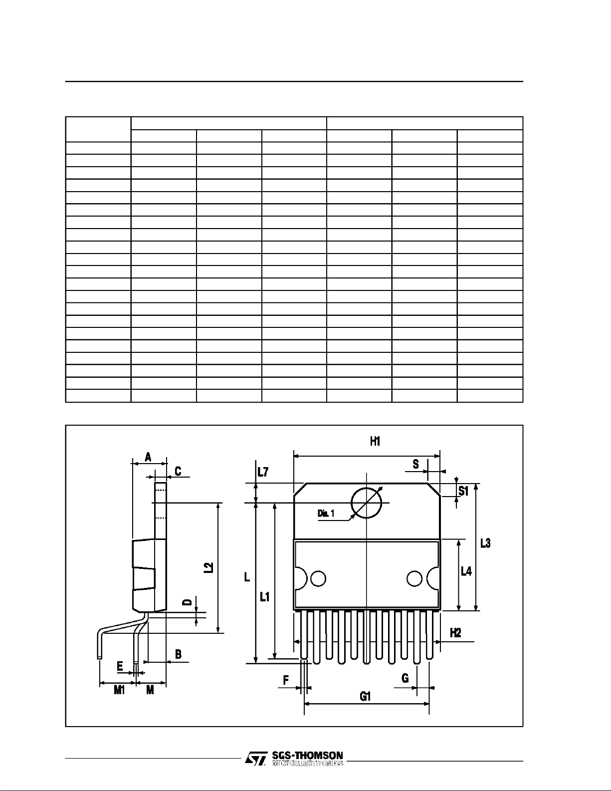
MULTIWATT11 PACKAGE MECHANICAL DATA
DIM.
A 5 0.197
B 2.65 0.104
C 1.6 0.063
D 1 0.039
E 0.49 0.55 0.019 0.022
F 0.88 0.95 0.035 0.037
G 1.45 1.7 1.95 0.057 0.067 0.077
G1 16.75 17 17.25 0.659 0.669 0.679
H1 19.6 0.772
H2 20.2 0.795
L 21.9 22.2 22.5 0.862 0.874 0.886
L1 21.7 22.1 22.5 0.854 0.87 0.886
L2 17.4 18.1 0.685 0.713
L3 17.25 17.5 17.75 0.679 0.689 0.699
L4 10.3 10.7 10.9 0.406 0.421 0.429
L7 2.65 2.9 0.104 0.114
M 4.25 4.55 4.85 0.167 0.179 0.191
M1 4.73 5.08 5.43 0.186 0.200 0.214
S 1.9 2.6 0.075 0.102
S1 1.9 2.6 0.075 0.102
Dia1 3.65 3.85 0.144 0.152
MIN. TYP. MAX. MIN. TYP. MAX.
mm inch
20/21

TDA2005
Information furnished is believed to be accurate and reliable. However, SGS-THOMSON Microelectronics assumes no responsibility for the
consequences of use of such information nor for any infringement of patents or other rights of third parties which may result fromits use. No
license is granted by implication or otherwise under any patent or patent rights of SGS-THOMSON Microelectronics. Specifications mentioned
in this publication are subject to change without notice. This publication supersedes and replaces all information previously supplied.
SGS-THOMSON Microelectronics products are notauthorized for use as critical componentsin life supportdevices orsystems without express
written approval of SGS-THOMSON Microelectronics.
1995 SGS-THOMSON Microelectronics - All Rights Reserved
MULTIWATTis aRegistered Trademark of SGS-THOMSON Microelectronics
Australia - Brazil -France - Germany - Hong Kong - Italy - Japan - Korea - Malaysia - Malta - Morocco - The Netherlands - Singa-
pore - Spain - Sweden - Switzerland - Taiwan - Thaliand - United Kingdom - U.S.A.
SGS-THOMSON Microelectronics GROUP OF COMPANIES
21/21
 Loading...