


10 + 10W STEREO AMPLIFIER FOR CAR RADIO
Its main featuresare :
Low distortion.
Low noise.
High reliabilityofthe chipand of thepackagewith
additionalsafetyduringoperationthanksto protections against:
.OUTPUTAC SHORTCIRCUIT TO GROUND
.VERYINDUCTIVE LOADS
.OVERRATINGCHIP TEMPERATURE
.LOADDUMP VOLTAGESURGE
.FORTUITOUS OPENGROUND
Spaceandcostsaving:verylownumberofexternalcomponents,verysimple mounting systemwith
noelectricalisolation betweenthe packageand the
heatsink.
DESCRIPTION
The TDA2004Ais a classB dual audio power amplifier in MULTIWATT
package specifically desi-
TDA2004A
MULTIWATT11
ORDERING NUMBER :TDA2004A
gnedforcarradioapplications;stereoamplifiersare
easily designed using this device that provides a
highcurrent capability(upto3.5A) andthatcandrive verylow impedanceloads(downto 1.6Ω ).
PIN CONNE CTIO N (top view)
March 1995
1/10
TD A200 4A
ABSOLUTE MAXIMUM RATINGS
Symbol Parameter Value Unit
OpeartingSupply Voltage 18 V
V
S
DC SupplyVoltage 28 V
V
S
Peak Supply Voltage (for 50ms) 40 V
V
S
(*) Output Peak Current(non repetitive t = 0.1ms) 4.5 A
I
O
(*) Output Peak Current(repetitive f ≥ 10Hz) 3.5 A
I
O
PowerDissipation at T
P
tot
,T
T
j
(*) The max. output current is internally limited.
Storageand JunctionTemperature –40 to150 °C
stg
THERMAL DATA
Symbol Parameter Value Unit
R
th j-case
ThermalResistance Junction-case Max. 3 °C/W
=60°C30W
case
ELECTRICAL CHARACTERISTICS (Refer to the test circuit, T
Rt
h (heatsink)
=4°C/W, unless otherwise specified)
=25°C, GV= 50dB,
amb
Symbol Parameter Test Condition Min. Typ. Max. Unit
SupplyVoltage 8 18 V
V
S
QuiescentOutput Voltage VS = 14.4V
V
O
TotalQuiescent Drain Current VS=14.4V
I
d
Stand-byCurrent Pin 3 grounded 5 mA
I
SB
OutputPower (eachchannel) f = 1KHz, d = 10%
P
O
V
=13.2V
S
V
=13.2V
S
V
=14.4V
S
R
=4Ω
L
R
=3.2Ω
L
R
=2Ω
L
R
= 1.6Ω
L
=13.2V
V
S
R
=3.2Ω
L
R
= 1.6Ω
L
=16V; RL=2Ω 12 w
V
S
6.6
6.0
6
7
9
10
6
9
7.2
6.6
65
62
6.5
8
10(*)
11
6.5
10
7.8
7.2
120
120
d Distortion (each channel) f = 1KHz
V
=14.4V; RL=4Ω
S
P
= 50mW to 4W
O
V
=14.4V; RL=2Ω
S
P
= 50mW to 6W
O
V
=13.2V; RL= 3.2Ω
S
P
= 50mW to 3W
O
V
=13.2V; RL= 1.6Ω
S
P
= 50mW to 6W
O
CT Cross Talk V
Input SaturationVoltage 300 mV
V
i
=14.4V
S
V
= 4Vrms RL=4Ω
O
f = 1KHz
f = 10KHz R
g
=5KΩ
50
40
0.2
0.3
0.2
0.3
60
45
1
1
1
1
V
V
mA
mA
W
W
W
W
w
w
%
%
%
%
dB
dB
2/10
TD A 2004A
ELECTRICAL CHARACTERISTICS (continued
Symbol Parameter Test Condition Min. Typ. Max. Unit
InputResistance (non invertinginput) f = 1KHz 70 200 KΩ
R
i
Low Frequency Roll off (-3dB) RL=4Ω
f
L
HighFrequency Roll off (-3dB) RL= 1.6Ω to 4Ω 15 KHz
f
H
Voltagegain (open loop) f = 1KHz 90 dB
G
V
Voltagegain (closed loop) f = 1KHz 48 50 51 dB
closedloop gainmatching 0.5 dB
TotalInput noise Voltage Rg= 10KΩ (**) 1.5 5 µV
e
N
SVR Supply Voltage Rejection f
η Efficiency V
T
Thermal Shutdown Junction
J
Temperature
Notes : (*) 9.3W without Bootstrap
(**) BandwithFilter: 22Hz to 22KHz.
R
=2Ω
L
R
= 3.2Ω
L
R
= 1.6Ω
L
=100Hz; Rg= 10KΩ
ripple
C3 = 10µFV
= 14.4V f = 1KHz
S
R
=4Ω PO=6.5W
L
R
=2Ω PO= 10W
L
V
= 13.2V f = 1KHZ
S
R
=3.2Ω PO=6.5W
L
R
= 1.6Ω PO=10W
L
ripple
35 45 dB
=0.5Vrms
70
60
70
60
145 °C
35
50
40
55
Hz
Hz
Hz
Hz
%
%
%
%
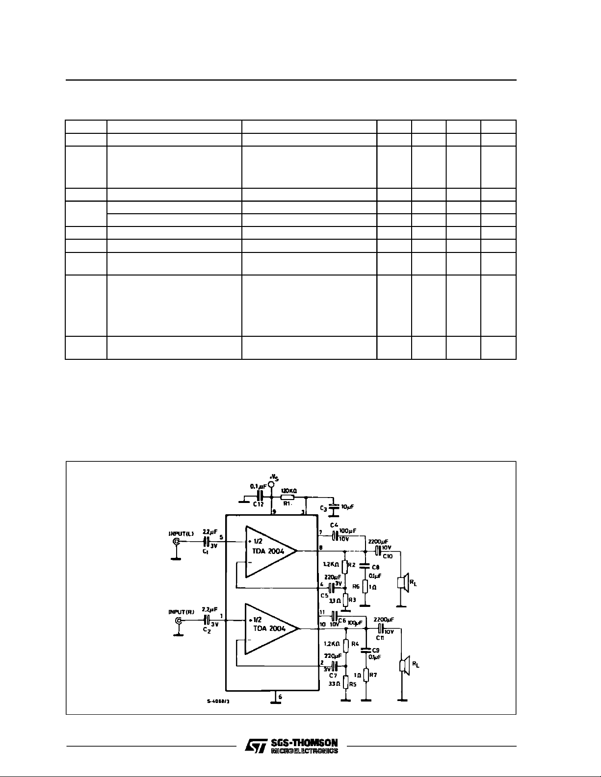
Figure 1 : Test an d App lica tion Circ u it .
3/10

TD A200 4A
Figure 2 : P.C. B oard and Component layout of the fig. 1 (scale 1 : 1).
Figure3 : QuiescentOutputVoltagevs.
SupplyVoltage.
4/10
Figure4 : QuiescentDrainCurrentvs.
SupplyVoltage.

Figure 6 : Output Powervs.Supply Voltage.Figure5 : Distortion vs. OutputPower.
Figure7 : OutputPower vs. SupplyVoltage. Figure 8 : Distortion vs. Frequency.
TD A 2004A
Figure9 : Distortion vs. Frequency. Figure10 : SupplyVoltageRejection vs. C
.
3
5/10

TD A200 4A
Figure 11 : SupplyVoltageRejectionvs.
Frequency.
Figure13 : SupplyVoltageRejection vs.
Valuesof CapacitorsC
and C3.
2
Figure12 : SupplyVoltageRejection vs.
Valuesof CapacitorsC
andC3.
2
Figure 14 : Gain vs. InputSensitivity.
Figure15 : MaximumAllowable Power
Dissipationvs. Ambient Temperature.
6/10
Figure16 : TotalPower Dissipationand
Efficiencyvs. OutputPower.

TD A 2004A
Figure17 : TotalPower Dissipationand
Efficiency vs. OutputPower .
APPL ICATI ON SUGGESTI O N
Therecommendedvaluesofthecomponentsare thoseshownonapplicationcircuitof fig.1.Differentvalues
can beused ; the followingtable canhelp the designer.
Component Recomm. Value Purpose LargerThan Smaller Than
R1 120KΩ Optimization of the
output signal simmetry
R2, R4 1KΩ Closeloop gain
R3, R5 3.3Ω Decreaseof gain Increase of gain
R6, R7 1Ω Frequencystability Danger of oscillation
C1, C2 2.2µF InputDC decoupling Highturn-on delay High turn-on pop
C3 10µF Ripple Rejection Increaseof SVR.
C4, C6 100µF Boostrapping Increaseof distortion
C5, C7 100µF Feedback Input DC
C8, C9 0.1µF FrequencyStability Danger of oscillation.
C10, C11 1000µF to 2200µF OutputDC decoupling. Higher low-frequency
setting(*)
decoupling.
Smaller P
Increaseof gain Decreaseof gain
at high frequency with
inductive load
Increaseof the switchon time.
max. SmallerPOmax.
O
Higher low frequency
cutoff. Increase of
noise
Degradation of SVR.
at low frequency
cut-off.
(*) The closed–loop gain must be higher than 26dB.
7/10

TD A200 4A
BUILT–IN PROTECTION SYSTEMS
LOADDUMP VOLTAGESURGE
TheTDA2004Ahasa circuit which enablesitto wi-
thstanda voltage pulsetrain, on pin 9, of the type
shownin Fig.19.
If thesupplyvoltage peaks to more than40 V, then
anLCfiltermustbeinsertedbetweenthesupplyand
pin9, in orderto assure thatthe pulsesat pin 9 will
be heldwithin thelimitsshown.
A suggestedLC networkis shownin Fig. 18. With
thisnetwork,atrainofpulsewithamplitudeupto120
V and with of 2 ms can be applied to point A. This
type of protection is ON when the supply voltage
(pulseorDC) exceeds18V.Forthisreasonthemaximumoperatingsupply voltageis 18 V.
Figure 1 8.
POLARITYINVERSION
Highcurrent(up to10A) can behandledby thede-
vice with no damage for a longer period than the
blow-outtime of a quick 2 Afuse (normallyconnected in series with thesupply).This featureis added
to avoiddestruction,if duringfittingto thecar, a mistakeon theconnectionof thesupplyis made.
OPENGROUND
Whenthe ratiois the ON conditionand the ground
is accidentally opened, a standard audio amplifier
will bedamaged.Onthe TDA2004Aprotectiondiodesare includedto avoidany damage.
INDUCTIVELOAD
A protection diode is provided to allow use of the
TDA2004Awith inductiveloads.
DCVOLTAGE
The maximum operating DC voltage on the
TDA2004Ais 18 V.
Howeverthe devicecan withstanda DCvoltageup
to28V withnodamage.Thiscouldoccurduringwinter iftwobatteriesareseriesconnectedtocrankthe
engine.
Figure 1 9.
SHORTCIRCUIT (ACconditions)
The TDA2004Acan withstandan accidental short-
circuit fromtheoutputto groundcausedbya wrong
connectionduringnormal working.
THERMALSHUT-DOWN
The presenceof a thermallimiting circuit offersthe
following advantages:
1)anoverloadontheoutput(evenif itispermanent),
or anexcessive ambienttemperaturecanbe easily
withstood.
2) the heatsinkcan have a smaller factorof safety
comparedwith that of a conventionalcircuit. There
is no device damagein the caseof excessivejunction temperature; all that happensis the P
thereforeP
)andIdarereduced.
tot
O
(and
Themaximumallowablepowerdissipationdepends
uponthesizeoftheexternalheatsink(i.e.itsthermal
resistance); fig. 15 shownthis dissipablepower as
a functionof ambienttemperaturefor differentthermalresistance.
8/10

MULTIWATT11 PACKAGE MECHANICAL DATA
TD A 2004A
DIM.
A 5 0.197
B 2.65 0.104
C 1.6 0.063
D 1 0.039
E 0.49 0.55 0.019 0.022
F 0.88 0.95 0.035 0.037
G 1.45 1.7 1.95 0.057 0.067 0.077
G1 16.75 17 17.25 0.659 0.669 0.679
H1 19.6 0.772
H2 20.2 0.795
L 21.9 22.2 22.5 0.862 0.874 0.886
L1 21.7 22.1 22.5 0.854 0.87 0.886
L2 17.4 18.1 0.685 0.713
L3 17.25 17.5 17.75 0.679 0.689 0.699
L4 10.3 10.7 10.9 0.406 0.421 0.429
L7 2.65 2.9 0.104 0.114
M 4.25 4.55 4.85 0.167 0.179 0.191
M1 4.73 5.08 5.43 0.186 0.200 0.214
S 1.9 2.6 0.075 0.102
S1 1.9 2.6 0.075 0.102
Dia1 3.65 3.85 0.144 0.152
MIN. TYP. MAX. MIN. TYP. MAX.
mm inch
9/10

TD A200 4A
Information furnished is believed to be accurate and reliable. However, SGS-THOMSON Microelectronics assumes no responsibility for
the consequences of use of such information nor for any infringement of patents or other rights of third parties which may result from its
use. No license is granted by implication or otherwise under any patent or patent rights of SGS-THOMSON Microelectronics. Specifications mentioned in this publication are subject to change without notice. This publication supersedes and replaces all information previously supplied. SGS-THOMSON Microelectronics products are not authorized for use as critical components in life support devices or
systems without express written approval of SGS-THOMSON Microelectronics.
1995 SGS-THOMSON Microelectronics - All Rights Reserved
MULTIWATT is a Registered Trademark of SGS-THOMSON Microelectronics
Australia - Brazil - France - Germany - Hong Kong - Italy - Japan - Korea - Malaysia - Malta - Morocco - The Netherlands - Singapore -
SGS-THOMSON Microelectronics GROUP OF COMPANIES
Spain - Sweden - Switzerland - Taiwan - Thaliand - United Kingdom - U.S.A.
10/10
 Loading...