

10W AUDIO AMPLIFIERWITHMUTING
DESCRIPTION
The TDA 1910 is a monolithicintegratedcircuit in
MULTIWATT package, intended for use in Hi-Fi
audiopowerapplications,as high quality TV sets.
The TDA 1910 meets the DIN 45500 (d = 0.5%)
guaranteed output power of 10W when used at
24V/4W.At 24V/8Wthe output power is 7W min.
Features:
– muting facility
– protection against chip overtemperature
– very low noise
– high supplyvoltage rejection
– low ”switch-on”noise.
The TDA 1910 is assembled in MULTIWATT
packagethat offers:
– easy assembly
– simple heatsink
Multiwatt 11
ORDERING NUMBERS
TDA1910 (Multiwatt11Vertical)
TDA1910HS (Multiwatt11 Horizontal)
– space and cost saving
– high reliability
TDA1910
:
ABSOLUTEMAXIMUM RATINGS
Symbol Parameter Value Unit
V
I
o
I
o
V
V
V
11
P
tot
T
stg,Tj
Supply voltage 30 V
s
Output peak current (non repetitive) 3.5 A
Output peak current (repetitive) 3.0 A
Input voltage 0 to + V
i
Differential input voltage
i
Muting thresold voltage V
Power dissipation at T
Storage and junction temperature -40 to 150
=90°C20W
case
7V
±
s
s
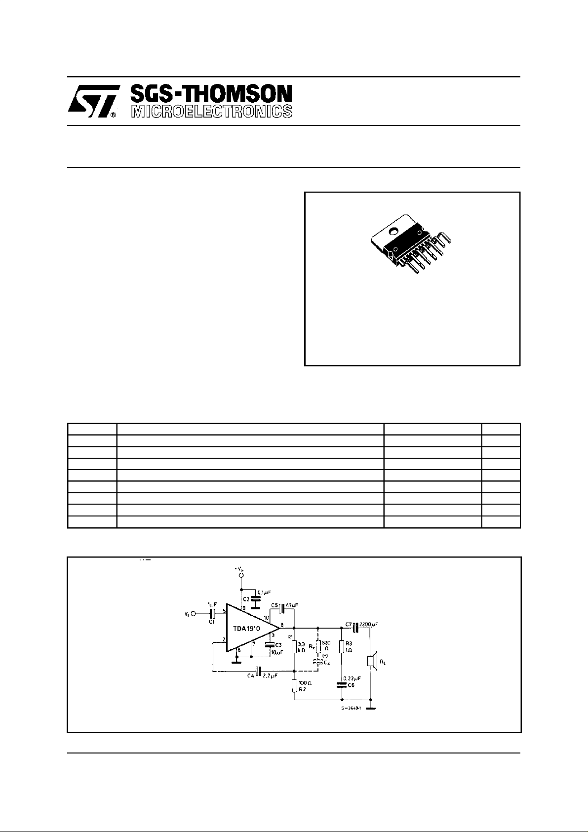
TESTCIRCUIT
V
V
C
°
May 1997
(*)Seefig. 13.
1/14
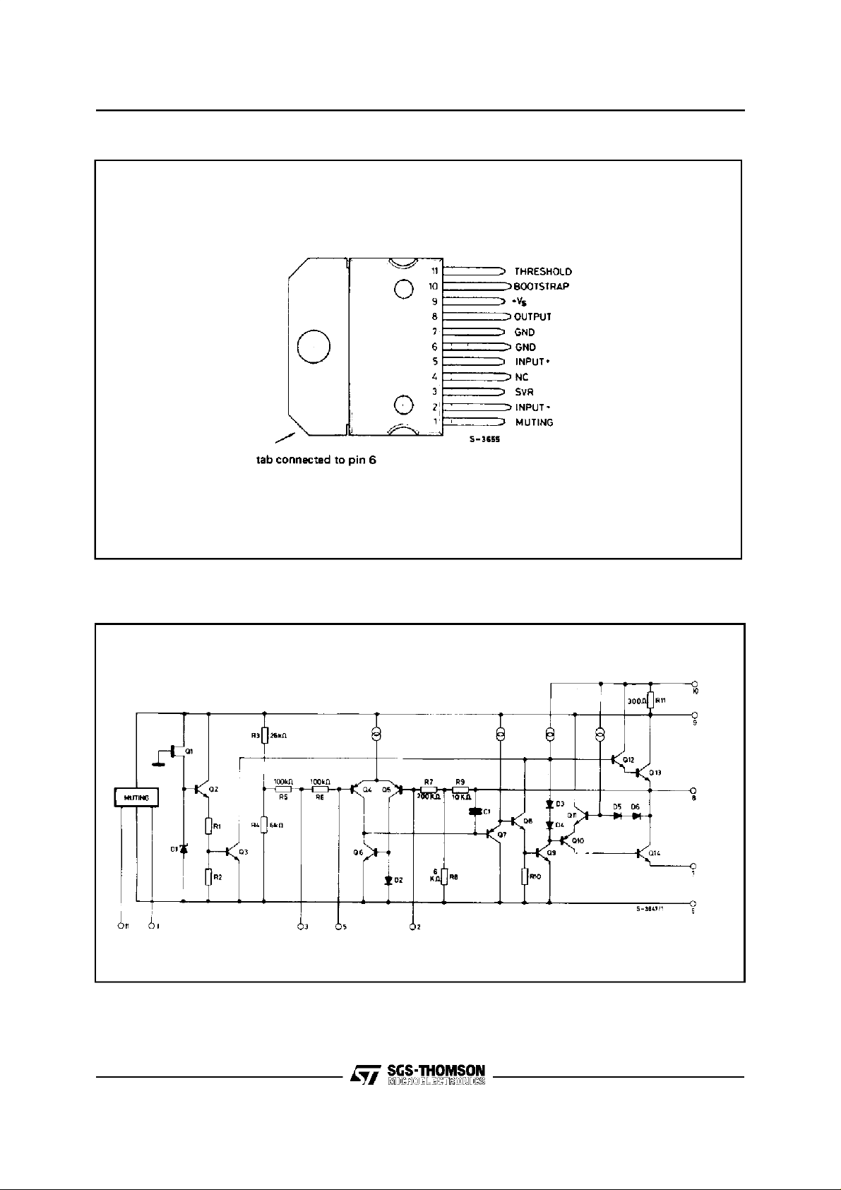
TDA1910
PIN CONNECTION
(Topview)
SCHEMATICDIAGRAM
2/14
TEST CIRCUIT
(*) See fig. 13.
TDA1910
MUTINGCIRCUIT
3/14

TDA1910
THERMALDATA
Symbol Parameter Value Unit
R
th j-case
Thermal resistance junction-case max 3
C/W
°
ELECTRICALCHARACTERISTICS(Refer tothetestcircuit, T
=25°C,Rth(heatsink)=4°C/W,unless
amb
otherwisespecified)
Symbol Parameter Test condition Min. Typ. Max. Unit
V
V
V
CE sat
P
Supply voltage 8 30 V
s
Quiescent output voltage Vs= 18V
o
I
Quiescent drain current Vs= 18V
d
V
V
= 24V
s
= 24V
s
8.3
11.5
9.2
12.41013.4
19
21
Output stage saturation voltage IC=2A 1
I
= 3A 1.6
C
Output power d = 0.5%
o
V
s
V
s
V
s
d = 10%
V
s
V
s
V
s
Harmonic distortion f = 40 to 15,000 Hz
d
Vs= 18V RL=4
V
s
V
s
= 18V
= 24V
= 24V
= 18V
= 24V
= 24V
= 24V RL=4
= 24V RL=8
f = 40 to 15,000Hz
=4
R
Ω
L
=4
R
Ω
L
=8Ω
R
L
f = 1 KHz
=4
R
Ω
L
=4
R
Ω
L
=8
R
Ω
L
Ω
= 50 mW to 6.5W
P
o
Ω
= 50 mW to 10W
P
o
Ω
=50mWto 7W
P
o
6.5
10
7
8.5
15
9
7
12
7.5
9.5
17
10
0.2
0.2
0.2
32
35
0.5
0.5
0.5
V
mA
V
W
%
d Intermodulation distortion V
V
Input sensitivity
i
V
Input saturation voltage (rms) Vs= 18V
i
R
Input resistance (pin 5) f = 1 KHz 60 100 K
i
I
Drain current Vs= 24V f = 1 KHz
d
4/14
= 24V RL=4ΩPo= 10W
s
f
= 250 Hz f2 = 8 KHz
1
(DIN 45500)
F = 1 KHz,
V
= 18V
s
v
= 24V
s
V
= 24V
s
V
= 24V
s
R
RL = 8Ω P
R
L
R
L
R
L
=4Ω Po= 12W
L
=4
Ω
=4Ω
=8Ω
P
P
P
o
=7W
o
=12 W
o
= 7.5W
o
= 7.5W
1.8
2.4
0.2 %
170
220
mV
245
820
mA
475
V
Ω

TDA1910
ELECTRICALCHARACTERISTICS(continued)
Symbol Parameter Test condition Min. Typ. Max. Unit
h Efficiency V
BW Small signal bandwidth V
BW Power bandwidth V
G
G
e
Voltagegain (open loop) f = 1 KHz 75 dB
v
Voltagegain (closed loop) Vs= 24V
v
Totalinput noise Rg=50
N
S/N Signal to noiseratio
SVR Supply voltage rejection V
= 24V f = 1 KHz
s
R
=4
Ω
L
=8
R
Ω
L
= 24V RL=4ΩPo= 1W 10 to 120,000 Hz
s
P
= 24V
s
= 12W
o
R
d≤5%
RL=4
f = 1 KHz
Po = 1W
L
=4
Po= 12W
Po= 7.5W
Ω
Ω
29.5 30 30.5 dB
Ω
=1KΩ(°)
R
g
= 10K
R
R
R
R
V
P
R
= 24V
s
= 12W
o
=4
L
Ω
R
R
R
R
= 24V RL = 4
s
= 100 Hz Rg = 10 K
f
ripple
Ω
g
=50Ω
g
=1KΩ(°°)
g
= 10K
Ω
g
= 10KΩ
g
=0 (°)97
g
= 10K
Ω
g
=0 (°°)93
g
Ω
50 60 dB
Ω
62
65
40 to 15,000 Hz
1.2
1.3
1.5
2.0
2.0
2.2
3.0
3.2
4.0
5.0
5.2
6.0
103
105
100
100
%
µ
µ
dB
dB
V
V
T
Thermal sjut-down case (*)
sd
temperature
MUTINGFUNCTION (Refer to Muting circuit)
V
V
R
R
A
Note :
(°) Weightingfilter = curve A.
(°
°) Filter with noise bandwidth:22 Hz to22 KHz.
(*) See fig. 29 and fig. 30.
Muting-offthreshold voltage
T
(pin 11)
Muting-on threshold voltage
T
(pin 11)
Input resistance (pin 1) Muting off 80 200 K
1
Input resistance (pin 11) 150 K
11
Muting attenuation Rg+R1=10KΩ 50 60 dB
T
P
= 8W 110 125 °C
tot
1.9 4.7 V
0 1.3
6V
s
Muting on 10 30 Ω
V
Ω
Ω
5/14

TDA1910
Figure 1. Quiescent output
voltage vs.supply voltage
Figure 4. Output power vs.
supplyvoltage
Figure 2. Quiescent drain
currentvs. supply voltage
Figure 5. Output power vs.
supply voltage
Figure 3. Open loop frequencyresponse
Fi gure 6. Di storti on vs.
output power
Fi gure 7. Di storti on vs.
output power
6/14
Figure 8. Output power vs.
frequency
Figure 9. Output power vs.
frequency

TDA1910
Figure 10. Output power vs.
input voltage
Figure 13. Values of capacitor C
and gain (G
vs. bandwidth (BW)
X
)
V
Figure 11. Output power vs.
inputvoltage
Figure 14. Supply voltage
rejectionvs. voltagegain
Figure 12. Total input noise
vs. source resistance
Figure 15. Supply voltage
rejection vs. source
resistance
Figure 16. Power dissipationand efficiencyvs.output
power
Figure 17. Power dissipationandefficiencyvs. output
power
Figure 18. Max power
dissipation v s. supply
voltage
7/14

TDA1910
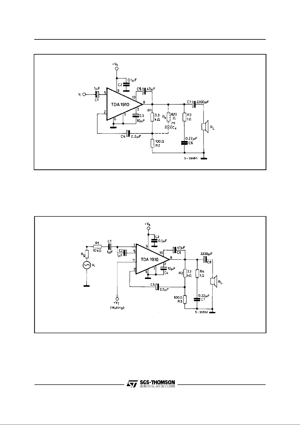
APPLICATIONINFORMATION
Figure19. Applicationcircuitwithout muting
Figure 20. PC boardand component lay-outof
the circuitof fig. 19 (1:1 scale)
Figure21. Applicationcircuitwith muting
8/14
Performance(circuitsof fig. 19 and 21)
=12W(40 to 15000Hz, d ≤ 0.5%)
P
o
= 24V
V
s
I
= 0.82A
d
G
=30dB
v

APPLICATIONINFORMATION(continued)
TDA1910
Figure22. TwopositionDC tonecontrol(10 dBboost 50Hz and
20 KHz) using change of pin 1 resistance(muting function)
Figure24. 10dB 50 Hz boos tonecontrolusing change of pin1
resistance(muting function)
Figure 23. Frequenc y response of the circuit of fig.22
Figure 25. Frequenc y response of the circuit of fig.24
Figure26. Squelchfunction in TV applications Figure 27. Delayed muting circuit
9/14

TDA1910
MUTINGFUNCTION
The output signal can be inhibitedapplying a DCvoltage V
Figure28
to pin 11,as shownin fig.28
T
The input resistanceat pin 1 dependson thethresholdvoltage V
= 200 K
R
1
R1 = 10 Ω
@ 1.9V≤V
Ω
@
0V ≤ V
6V ≤ VT≤ V
4.7V muting-off
≤
T
≤ 1.3V
T
s
muting-on
at pin 11and is typically.
T
Referringtothefollowinginputstage, thepossibleattenuationof theinputsignalandthereforeoftheoutput
signalcan be found using the following expression.
R
⁄⁄
R
⁄⁄
5
1
R
1
Considering Rg = 10 KΩ the attenuation in the
muting-on condition is typicallyA
= 60 dB. In the
T
muting-off condition, the attenuation is very low,
typically 1.2dB.
Avery low current is necessaryto drivethe threshold voltageV
becausethe input resistance at pin
T
11is greaterthan150 KΩ. Themutingfunction can
beusedinmanycases,whenatemporaryinhibition
V
R
=
≅
100
+
g
R
5
K
Ω
=
A
T
V
where R5
i
5
- during commutationsat the input stages.
- during the receivertuning.
The variable impedance capabilityat pin 1 can be
useful in many applications and we haveshown 2
examplesin fig.22 and 24,where it hasbeen used
tochangethe feedbacknetwork,obtaining2 different frequencyresponses.
of the output signal is requested,for example:
- in switch-on condition, to avoid preamplifier
power-on transients(see fig. 27)
10/14

TDA1910
APPLICATIONSUGGESTION
The recommended values of the components are those shown on applicationcircuit of fig. 21. Different
valuescan be used.
The followingtablecan helpthe designer.
Component
R
g+R1
R
2
R
3
R
4
P
1
C
1
C
2
C
3
C
4
C
5
Raccom.
value
10K
Ω
Purpose
Input signal imped.
for muting operation
3.3KΩ Close loop gain
setting.
100
Close loop gain
Ω
setting.
1
20K
Frequency stability Danger of oscillation
Ω
Volume
Ω
potentiometer.
1 µF
Input DC decoupling. Higher low frequency
1µF
0.22µF
2.2µF Inverting input DC
decoupling.
0.1µF Supply voltage
bypass.
Larger than
recommended value
Increase of the attenuation in muting-on
condition. Decrease
Smaller than
recommended value
Decrease of the
attenuation in muting
on condition.
Allowed range
Min. Max.
of the inputsensitivity.
Increase of gain. Decrease of gain.
Increase quiescent
9R
3
current.
Decrease of gain. Increase of gain. R2/9
at high frequencies
with inductive loads.
Increase of the
switch-on noise.
Decrease of the input
impedance and of the
10K
100K
Ω
input level.
cutoff.
Increase of the
switch-on noise.
Higher low frequency
cutoff.
0.1µF
Danger of oscillations.
Ω
C
6
10µF Ripple rejection. Increase of SVR.
Increase of the
Degradation of
SVR
2.2µF 100µF
switch-on time
C
7
47µF Bootstrap. Increase of the distor-
10µF 100µF
tion at low frequency.
C
8
C
9
0.22µF Frequency stability. Danger of oscillation.
2200µF
(R
=4Ω)
L
Output DC
decoupling.
Higher low frequency
cutoff.
1000µF
=8Ω)
(R
L
11/14

TDA1910
THERMALSHUT-DOWN
The presence ofa thermallimiting circuit offersthe
followingadvantages:
1) An overload on the output (even if it is permanent), or an above limit ambient temperature
can be easily supportedsince the T
cannotbe
j
higher than 150°C.
2) The heatskink can have a smaller factor of
safety compared with that of a conventional
Figure 29. Output power and
drai n curre nt vs. case
temperature
Figure 30. Output power and
drai n curre nt vs. case
temperature
circuit.Thereis no possibilityof devicedamage
due to high junction temperature.
If for any reason, the junction temperature increases up to 150°C, the thermal shut-down
simply reduces the power dissipation and the
currentconsumption.
The maximum allowable power dissipation dependsupon thesizeof theexternalheatsink(i.e.its
thermal resistance); fig. 31 shows this dissipable
power as a function of ambient temperature for
differentthermalresistance.
Figure31.Maximumallowable
powerdissipation vs. ambient
temperature
MOUNTINGINSTRUCTIONS
The power dissipated in the circuit must be removedby addingan externalheatsink.
Thanks to the Multiwatt package attaching the
heatsinkis verysimple, ascrewor a compression
12/14
spring(clip) beingsufficient.Between theheatsink
andthepackageitisbettertoinsertalayerofsilicon
grease,to optimizethe thermalcontact;no electrical isolationis neededbetweenthe two surfaces.

MULTIWATT 11VERTICAL PACKAGE MECHANICAL DATA
DIM.
MIN. TYP. MAX. MIN. TYP. MAX.
A 5 0.197
B 2.65 0.104
C 1.6 0.063
D 1 0.039
E 0.49 0.55 0.019 0.022
F 0.88 0.95 0.035 0.037
G 1.57 1.7 1.83 0.062 0.067 0.072
G1 16.87 17 17.13 0.664 0.669 0.674
H1 19.6 0.772
H2 20.2 0.795
L 21.5 22.3 0.846 0.878
L1 21.4 22.2 0.843 0.874
L2 17.4 18.1 0.685 0.713
L3 17.25 17.5 17.75 0.679 0.689 0.699
L4 10.3 10.7 10.9 0.406 0.421 0.429
L7 2.65 2.9 0.104 0.114
M 4.1 4.3 4.5 0.161 0.169 0.177
M1 4.88 5.08 5.3 0.192 0.200 0.209
S 1.9 2.6 0.075 0.102
S1 1.9 2.6 0.075 0.102
Dia1 3.65 3.85 0.144 0.152
mm inch
TDA1910
13/14

TDA1910
Information furnished is believed to be accurate and reliable. However, SGS-THOMSON Microelectronics assumes no responsibility for the
consequences of use of such information nor forany infringementof patents orother rights of third partieswhich may result from its use. No
license is granted by implicationor otherwiseunder any patentor patentrights of SGS-THOMSON Microelectronics. Specificationmentioned
in this publication are subject to change without notice. This publication supersedes and replaces all information previously supplied.
SGS-THOMSONMicroelectronics products arenot authorizedfor use as criticalcomponents in lifesupport devicesor systems withoutexpress
written approval of SGS-THOMSONMicroelectronics.
1997 SGS-THOMSON Microelectronics – Printedin Italy– All Rights Reserved
SGS-THOMSON Microelectronics GROUP OF COMPANIES
Australia - Brazil- Canada- China - France - Germany- Hong Kong - Italy- Japan - Korea - Malaysia- Malta - Morocco - TheNetherlands -
Singapore - Spain - Sweden - Switzerland- Taiwan- Thailand - United Kingdom - U.S.A.
14/14
 Loading...