

TDA1905
5W AUDIO AMPLIFIER WITH MUTING
DESCRIPTION
The TDA1905 is a monolithicintegrated circuit in
POWERDIP package, intended for use as low
frequencypower amplifierin a wide rangeof applications in radio and TV sets:
– muting facility
– protectionagainst chip over temperature
– very low noise
– high supply voltage rejection
– low ”switch-on” noise
– voltagerange 4V to 30V
TheTDA 1905is assembled in a new plasticpack-
age,thePOWERDIP,thatoffersthesameassembly
ease,spaceandcostsavingof a normaldualin-line
packagebutwithapowerdissipationofupto6Wand
ORDERING NUMBER : TDA1905
a thermalresistance of 15°C/W (junctionto pins).
ABSOLUTE MAXIMUMRATINGS
Symbol Parameter Value Unit
V
s
I
o
I
o
V
V
V
11
P
tot
T
stg,Tj
Supply voltage 30 V
Output peak current (non repetitive) 3 A
Output peak current (repetitive) 2.5 A
Input voltage 0 to + V
i
Differential input voltage
i
Muting thresold voltage V
Power dissipation at T
Storage and junction temperature -40 to 150
=80°C
amb
=60°C6W
T
case
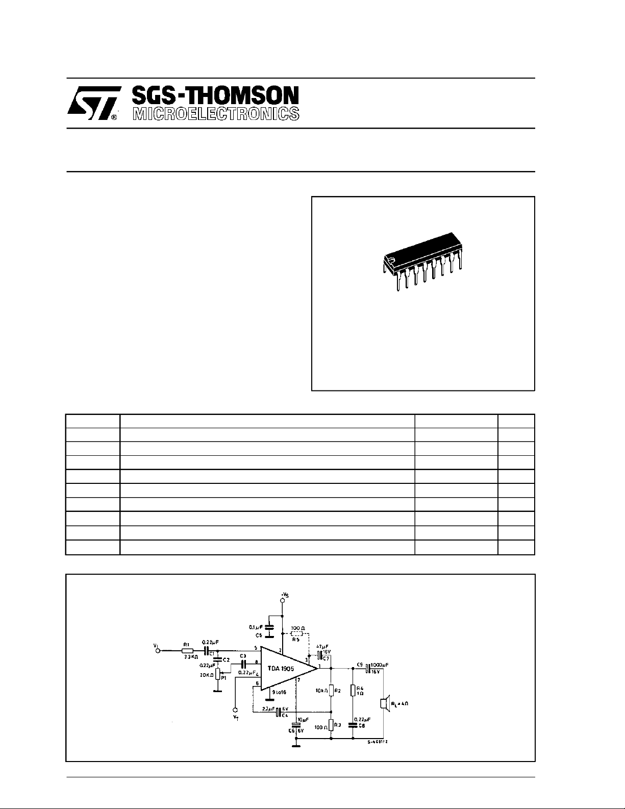
APPLICATION CIRCUIT
Powerdip
(8 + 8)
s
± 7
s
1W
V
V
V
°C
March 1993
1/14
TDA1905
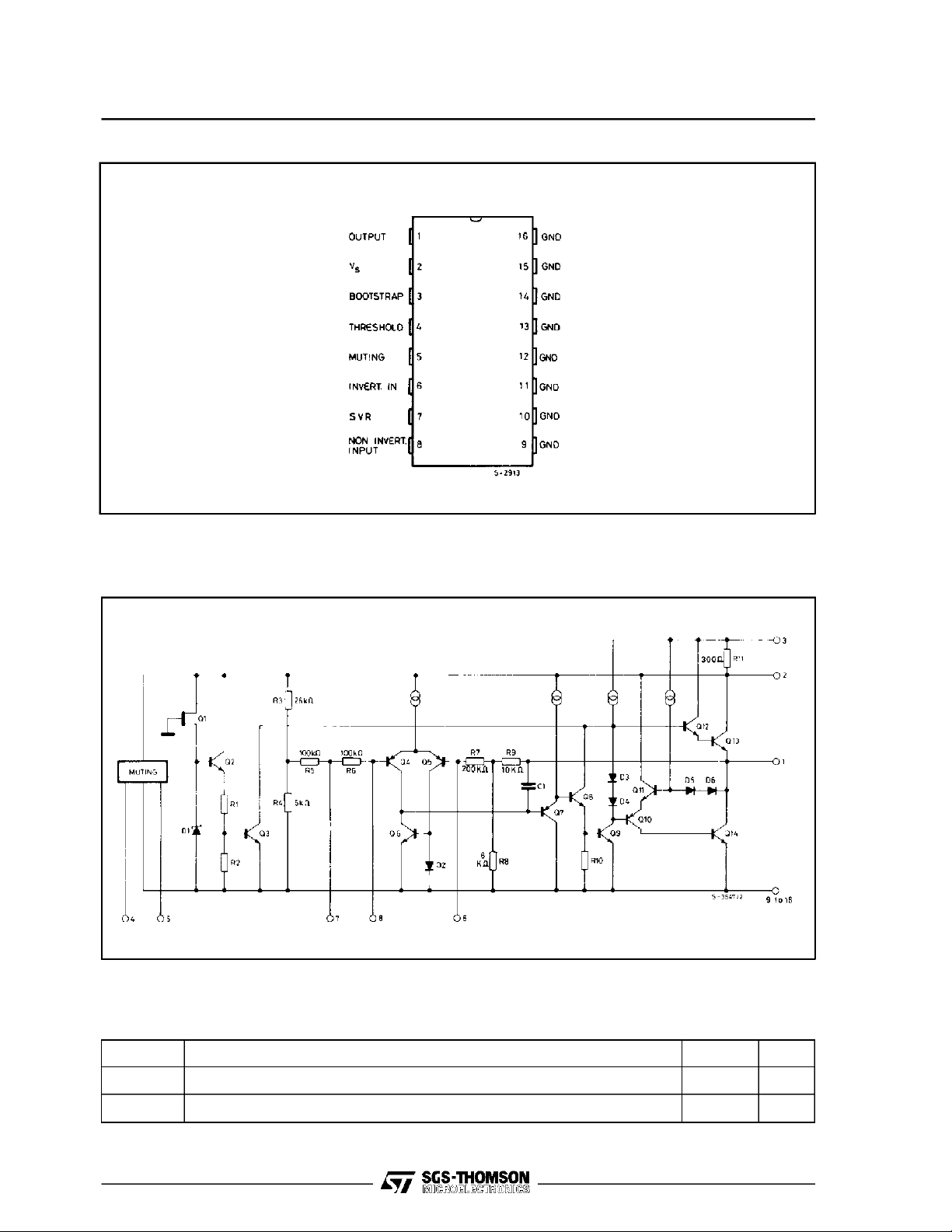
PIN CONNECTION (top view)
SCHEMATIC DIAGRAM
THERMALDATA
Symbol Parameter Value Unit
2/14
R
th-j-case
R
th-j-amb
Thermal resistance junction-pins max 15
Thermal resistance junction-ambient max 70
°C/W
°C/W

TEST CIRCUITS:
WITHOUTMUTING
TDA1905
WITH MUTING FUNCTION
3/14

TDA1905
ELECTRICAL CHARACTERISTICS (Referto the test circuit, T
=25°C, Rth(heatsink)= 20 °C/W,
amb
unless otherwiswspecified)
Symbol Parameter Test conditions Min. Typ. Max. Unit
Supply voltage 4 30 V
s
Quiescent output voltage Vs=4V
o
I
Quiescent drain current Vs=4V
d
Output stage saturation
V
= 14V
s
V
= 30V
s
V
= 14V
s
= 30V
V
s
IC=1A
1.6
6.7
14.4
2.1
7.2
15.5
15
17
21 35
0.5
voltage
Output power d = 10%
o
d Harmonic distortion
=2A
I
C
f = 1KHz
V
V
V
V
=9V
s
= 14V
s
= 18V
s
= 24V
s
R
R
R
R
f = 1KHz
V
=9V RL=4Ω
s
P
= 50 mW to 1.5W
V
V
V
s
s
s
o
= 14V RL=4Ω
P
=50mWto3W
o
= 18V RL=8Ω
=50mWto3W
P
o
= 24V RL=16Ω
P
=50mWto3W
o
=4Ω(*)
L
=4Ω
L
=8Ω
L
=16Ω
L
2.2
5
5
4.5
1
2.5
5.5
5.5
5.3
0.1
0.1
0.1
0.1
2.5
7.8
16.8
V
V
V
CE sat
P
V
mA
V
W
%
Input sensitivity f = 1KHz
V
i
V
Input saturation
i
voltage (rms)
R
Input resistance (pin 8) f = 1KHz 60 100
i
I
Drain current f = 1KHz
d
V
=9V
s
V
= 14V
s
V
= 18V
s
V
= 24V
s
Vs=9V
V
= 14V
s
V
= 18V
s
V
= 24V
s
V
=9V
s
V
= 14V
s
V
= 18V
s
V
= 24V
s
f = 1KHz
V
=9V
Efficiency
η
(*) With an external resistor of 100Ω between pin 3 and +Vs.
V
V
V
s
= 14V
s
= 18V
s
= 24V
s
R
R
R
R
R
R
R
R
R
R
R
R
L
L
L
L
L
L
L
L
L
L
L
L
=4Ω
=4Ω
=8Ω
=16Ω
=4Ω
=4Ω
=8Ω
=16Ω
=4Ω
=4Ω
=8Ω
=16Ω
P
P
P
P
P
P
P
P
P
P
P
P
o
o
o
o
o
o
o
o
o
o
o
o
= 2.5W
= 5.5W
= 5.5W
= 5.3W
= 2.5W
= 5.5W
= 5.5W
= 5.3W
= 2.5W
= 5.5W
= 5.5W
= 5.3W
0.8
1.3
1.8
2.4
37
49
73
100
380
550
410
295
73
71
74
75
mV
V
KΩ
mA
%
4/14
TDA1905
ELECTRICALCHARACTERISTICS (continued)
Symbol Parameter Testconditions Min. Typ. Max. Unit
BW Small signal
bandwidth (-3dB)
G
G
e
Voltagegain (open loop) Vs= 14V
v
Voltagegain (closed loop) Vs= 14V
v
Totalinput noise
N
S/N Signal to noiseratio
SVR Supply voltage rejection V
T
Thermal shut-down
sd
case temperatura
(*)
= 14V
V
s
=4Ω P
R
L
f = 1KHz
R
=4Ω
f = 1KHz
V
= 14V
s
= 5.5W
P
o
R
=4Ω
L
= 18V RL=8Ω
s
f
= 100 Hz Rg = 10KΩ
ripple
V
= 0.5V
ripple
L
=1W
P
o
R
=50Ω
g
R
=1KΩ
g
R
= 10KΩ
g
=50Ω
R
g
R
=1KΩ
g
R
= 10KΩ
g
R
= 10KΩ
g
R
=0 (°)
g
= 10KΩ
R
g
R
=0 (°°)
g
rms
P
tot
= 1W 40 to 40,000 Hz
o
75 dB
39.5 40 40.5 dB
1.2
(°)
1.3
1.5 4.0
2.0
(°°)
2.0
2.2 6.0
90
92 dB
87
87
40 50 dB
= 2.5W 115
µV
µV
dB
°C
MUTING FUNCTION
VT
VT
R
R
A
Note:
(°) Weighting filter= curve A.
(° °) Filterwith noise bandwidth: 22 Hz to 22 KHz.
(*) See fig. 30 and fig. 31
Muting-off threshold
OFF
voltage (pin 4)
Muting-on threshold
ON
voltage (pin 4)
Input-resistance (pin 5) Muting off 80 200
5
Input resistance (pin 4) 150
4
Muting attenuation
T
R
g+R1
1.9 4.7 V
0 1.3 V
6.2 V
Muting on 10 30
= 10KΩ
50 60 dB
s
KΩ
Ω
KΩ
5/14

TDA1905
Figure 1. Quiescent output
voltagevs. supply voltage
Fig ure 4. Dis tort ion vs.
output power (R
=16Ω)
L
Figure 2. Quiescent drain
current vs. supply voltage
Figur e 5 . Dis tortion v s.
output power (RL=8Ω)
Figure 3. Output power vs.
supply voltage
Figur e 6 . D isto rtion vs .
outputpower (RL=4Ω)
Fig ure 7. Dis tort ion vs.
frequency (R
6/14
=16Ω)
L
Figur e 8 . Dis tortion v s.
frequency(RL=8Ω)
Figur e 9 . D isto rtion vs .
frequency(RL=4Ω)

TDA1905
Figure 10. Open loop frequencyresponse
Figure13. Supply voltagerejection vs. voltage gain (ref.
to the Muting circuit)
Figure 11. Output power vs.
inputvoltage
Figure14.Supply voltagereectionvs. source resistance
Figure 12. Value of capacitor Cx vs. bandwidth (BW)
and gain (Gv)
Figure 15. Max power dissipation vs. supply voltage
(sine wave operation)
Figure 16. Power dissipationand efficiencyvs. output
power
Figure 17. Power dissipationand efficiencyvs. output
power
Figure 18. Power dissipationand efficiencyvs. output
power
7/14

TDA1905
APPLICATIONINFORMATION
Figure 19. Applicationcircuit without muting
Figure 20. PC board and components lay-out
of the circuit of fig. 19 (1 : 1scale)
Figure21. Applicationcircuit withmuting
Figure 22. Delayed muting circuit
8/14

APPLICATIONINFORMATION (continued)
TDA1905
Figure23. Low-cost applicationcircuit without bootstrap.
Figure 25. Two position DC tonecontrol using change of
pin 5 resistance(muting function)
Figure 24. Output power
vs. supply voltage (circuit
of fig. 23)
Figure 26. Frequency responseofthe circuitoffig.25
Figure 27. Bass Bomb tone controlusingchange of pin 5
resistance(muting function)
Figure 28. Frequency responseofthecircuitoffig. 27
9/14

TDA1905
MUTING FUNCTION
The outputsignal can be inhibitedapplying a DC voltage V
to pin 4, as shownin fig. 29
T
Figure29
The input resistanceat pin 5 depends on the thresholdvoltageV
= 200 KΩ @ 1.9V ≤ VT≤ 4.7V muting-off
R
5
R5 = 10 Ω @
0V ≤ VT ≤ 1.3V
6V ≤ VT ≤ V
s
at pin4 and is typically :
T
muting-on
Referringto the followinginputstage,thepossibleattenuationof the inputsignalandthereforeof the output
signal can be found using the following expression:
•
R
R
8
5
R
5
)
)
5
+(
R
g
V
i
=
A
T
=
V
8
R8+5
R
8
(
R8+R
•
where R8 ≅ 100 K Ω
Considering R
muting-on condition is typicallyA
=10KΩ the attenuationin the
g
= 60 dB. In the
T
muting-off condition, the attenuation is very low,
typically1.2 dB.
A very low current is necessarytodrive the threshold voltage V
because the input resistance at pin
T
4 is greaterthan 150 KΩ. Themutingfunction can
beusedinmanycases ,whena temporaryinhibit ion
– duringswitching at the input stages.
– duringthe receiver tuning.
The variableimpedance capabilityat pin 5 canbe
usefulin manyapplications and two examples are
shownin fig. 25 and27, whereit hasbeenusedto
change thefeedbacknetwork, obtaining2different
frequencyresponses.
of the output signal is requested, for example:
– in switch-on condition, to avoid preamplifier
power-ontransients(seefig. 22)
10/14

TDA1905
APPLICATIONSUGGESTION
The recommendedvalues of the external componentsarethoseshownonthe applicationcircuitof fig. 21.
When the supply voltageV
in order to obtain the maximumoutput power.
Differentvalues can be used. The followingtable can help the designer.
is less than 10V,a100Ω resistormustbe connected betweenpin 2 and pin 3
s
Component
R
g+R1
R
2
R
3
R
4
R
5
P
1
C
1
C
2
C
3
Raccom.
value
Purpose
10KΩ Inputsignal imped.
for muting operation
Larger than
recommended value
Increase of the
attenuation in muting-on
condition. Decrease of
the input sensitivity.
10KΩ
Increase of gain. Decrease of gain.
Feedback resistors
100Ω
Decrease of gain. Increase ofgain.
1KΩ Frequency stability Danger of oscillation at
high frequencies with
inductive loads.
100Ω Increase of theoutput
swingwith low supply
voltage.
20KΩ Volumepotentiometer Increase of the
switch-on noise.
0.22µF
InputDC
decoupling.
Higher cost
lower noise.
Smaller than
recommended value
Decrease of the attenuation inmuting on
condition.
Increase quiescent
current.
Decrease of the input
impedance and of the
input level.
Higher low
frequency cutoff.
Higher noise.
Allowed range
Min. Max.
9R
3
1KΩ
47 330
10KΩ 100KΩ
C
4
C
5
C
6
2.2µF Invertinginput DC
decoupling.
0.1µF
Supplyvoltage
bypass.
10µF
Ripple rejection Increase of SVR
Increase of the switchon noise.
Higher low frequency
cutoff.
Danger of
oscillations.
Degradation of SVR
0.1µF
2.2µF 100µF
increase of the
switch-on time
C
7
47µF Bootstrap. Increase ofthe
10µF 100µF
distortion at low
frequency.
C
8
C
9
0.22µF
1000µF
Frequency stability. Danger of oscillation.
Output DC decoupling. Higher low frequency
cutoff.
11/14

TDA1905
THERMALSHUT-DOWN
The presence of a thermal limiting circuit offers the followingadvantages:
1) Anoverloadon theoutput (even if itis permanent),oran abovelimitambienttemperature canbeeasily
tolerated since the Tj cannotbe higher than 150 °C.
2) The heatsink can have a smallerfactor of safety compared with that of a conventionalcircuit. There is
no possibility of device damage due to high junction temperature.
Ifforanyreason,thejunctiontemperatureincreasesupto 150°C,thethermalshut-downsimplyreduces
the power dissipation and the current consumption.
The maximumallowable powerdissipationdependsupon the size of the externalheatsink (i.e. its thermal
resistance);fig. 32shows this dissipable power as a functionof ambient temperaturefor differentthermal
resistance.
Figure 30. Output power
and drain current vs. case
temperature
Figure 31. Output power
and drain current vs. case
temperature
MOUNTINGINSTRUCTION : See TDA1904
Figure 32. Maximum allowable power dissipation
vs. ambient temperature
12/14

POWERDIPPACKAGE MECHANICAL DATA
TDA1905
DIM.
MIN. TYP. MAX. MIN. TYP. MAX.
a1 0.51 0.020
B 0.85 1.40 0.033 0.055
b 0.50 0.020
b1 0.38 0.50 0.015 0.020
D 20.0 0.787
E 8.80 0.346
e 2.54 0.100
e3 17.78 0.700
F 7.10 0.280
I 5.10 0.201
L 3.30 0.130
Z 1.27 0.050
mm inch
13/14

TDA1905
Information furnished is believed to be accurate and reliable. However, SGS-THOMSON Microelectronics assumes no responsibility for the
consequences of use of such information nor for any infringement of patents or otherrights of third parties which may result from its use. No
license is granted by implication or otherwise under any patent or patent rightsof SGS-THOMSON Microelectronics. Specificationsmentioned
in this publication are subject to change without notice. This publication supersedes and replaces all information previously supplied.
SGS-THOMSON Microelectronics products are notauthorized foruse ascritical components inlife supportdevices or systems without express
written approval of SGS-THOMSON Microelectronics.
1994 SGS-THOMSONMicroelectronics - All RightsReserved
SGS-THOMSON Microelectronics GROUP OF COMPANIES
Australia - Brazil - France - Germany - Hong Kong - Italy - Japan - Korea - Malaysia - Malta-Morocco - The Netherlands - Singapore -
Spain - Sweden - Switzerland - Taiwan- Thaliand -United Kingdom - U.S.A.
14/14
 Loading...