

TDA1904
4WAUDIOAMPLIFIER
HIGHOUTPUTCURRENTCAPABILITY
PROTECTION AGAINST CHIP OVERTEM-
PERATURE
LOWNOISE
HIGHSUPPLY VOLTAGEREJECTION
SUPPLY VOLTAGERANGE: 4V TO 20V
DESCRIPTION
The TDA 1904 is a monolithicintegrated circuit in
POWERDIP package intended for use as low-frequency power amplifier in wide range of applica-
ORDERING NUMBER
tions in portableradio and TV sets.
ABSOLUTEMAXIMUM RATINGS
Symbol Parameter Value Unit
V
S
I
O
I
O
P
tot
T
stg,Tj
Supply voltage 20 V
Peak output current (non repetitive) 2.5 A
Peak output current (repetitive) 2 A
Totalpower dissipation at T
Storage and junction temperature -40 to 150
at T
amb
pins
=80°C
=60°C
Powerdip
(8 + 8)
: TDA1904
1W
6W
°C
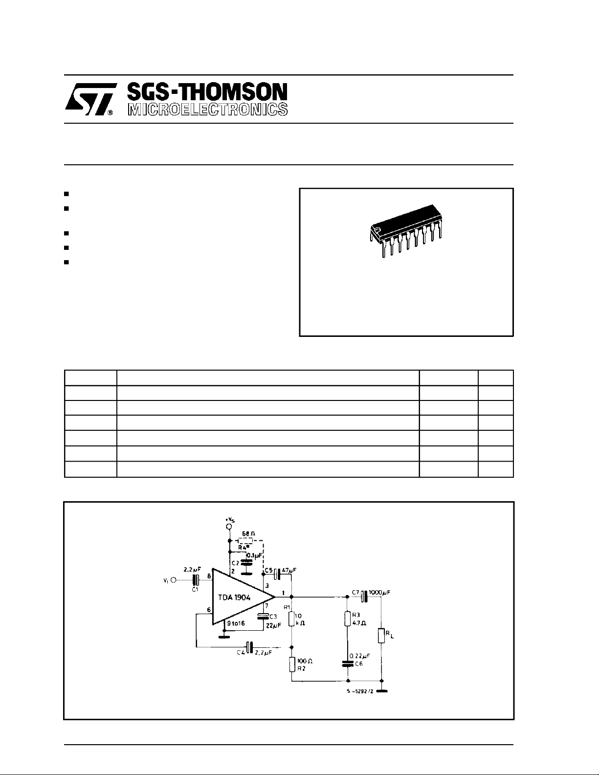
TEST AND APPLICATIONCIRCUIT
(*) R4 is necessaryonly for V
March 1993
<6V.
s
1/10
TDA1904
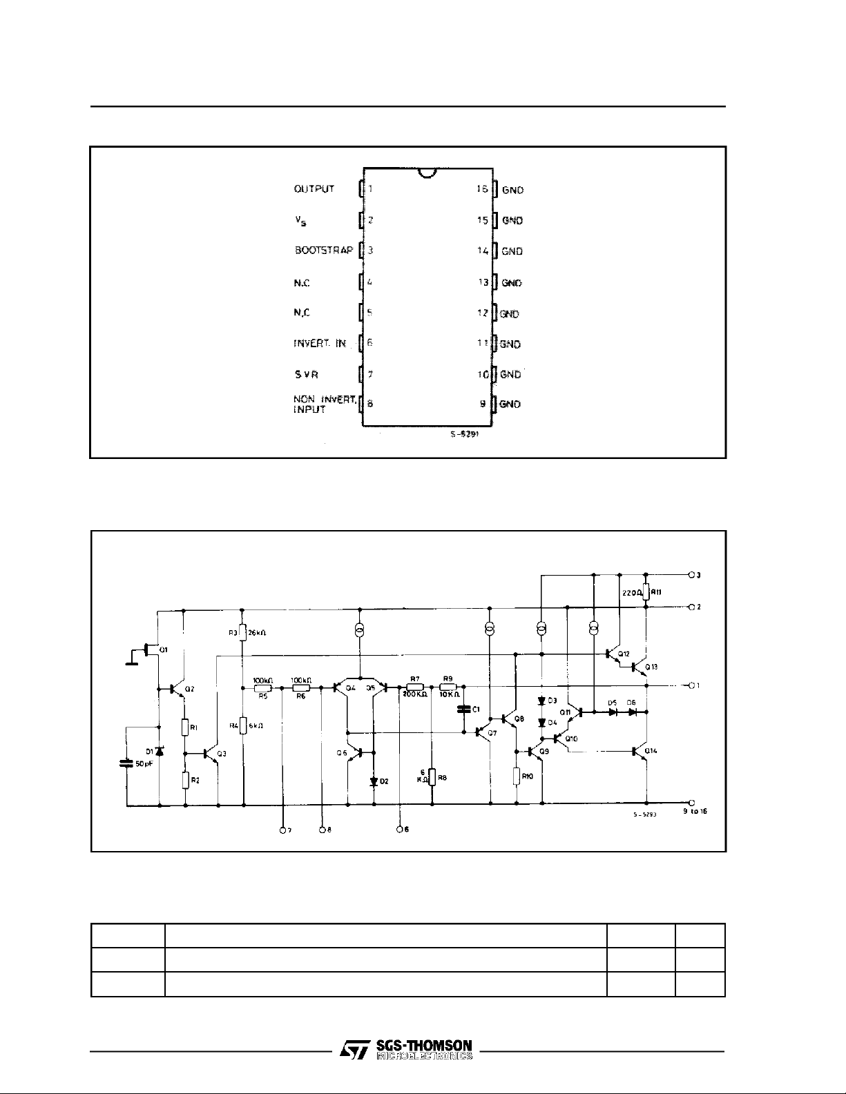
PIN CONNECTION (top view)
SCHEMATICDIAGRAM
THERMALDATA
Symbol Parameter Value Unit
2/10
R
th-j-case
R
th-j-amb
Thermal resistance junction-pins max 15
Thermal resistance junction-ambient max 70
C/W
°
°C/W

TDA1904
ELECTRICALCHARACTERISTICS (Refer to the test circuit, T
=25°C, Rth(heatsink)=
amb
20 °C/W, unless otherwiswspecified)
Symbol Parameter Testconditions Min. Typ. Max. Unit
V
V
I
P
d Harmonic distortion
V
R
η
BW Small signal bandwidth(-3 dB) V
G
Supply voltage 4 20 V
s
Quiescent output voltage
o
Quiescent drain current Vs=9V
d
Output power d = 10%
o
V
V
V
V
V
V
V
=4V
s
= 14V
s
= 14V
s
=9V
s
= 14V
s
= 12V
s
=6V
s
f = 1 KHz
R
=4
Ω
L
1.8
4
3.1
0.7
2.1
7.2
8
10
2
4.5 W
f = 1 KHz
V
=9V RL=4
s
= 50 mW to 1.2W
P
o
Input saturation voltage
i
(rms)
Input resistance (pin 8) f = 1 KHz 55 150
i
Efficiency
Voltagegain (open loop)
v
Vs=9V
V
= 14V
s
f = 1 KHz
V
=9V RL=4
s
V
= 14V RL=4Ω Po= 4.5W
s
= 14V
s
= 14V
V
s
Ω
R
L
f = 1 KHz
Po=2W
=4
Ω
Ω
0.8
1.3
0.1 0.3 %
70
65
40 to 40,000 Hz
75 dB
15
18
V
mA
V
KΩ
%
G
e
Voltagegain (closed loop) Vs= 14V
v
Total input noise Rg=50
N
SVR Supply voltage rejection V
T
Thermal shut-down case
sd
temperature
Note: (°) Weightingfilter = curve A.
(°°) Filterwith noise bendwidth: 22Hz to 22 KHz.
=4Ω
R
f = 1 KHz
Ω
R
=10KΩ
g
R
=50
Ω
g
R
=10KΩ
g
= 12V
s
f
= 100 Hz
ripple
V
= 0.5 Vrms
ripple
P
= 2W 120 ÉC
tot
P
R
L
=1W
o
g
(°)
(°°)
=10KΩ
39.5 40 40.5 dB
1.2
24
2
3
40 50 dB
µV
µV
3/10

TDA1904
Figure 1. Testand application circuit
(*) R4 is necessary only for VS<6V
Figure 2. P.C. boardand components layoutof fig. 1 (1 : 1 scale)
4/10

APPLICATION SUGGESTION
The recommended values of the external components are those shown on the application circuitof
fig. 1.
Whenthe supplyvoltageV
isless than 6V,a 68Ω
S
resistor must be connected betweenpin 2 andpin
TDA1904
3 in order to obtain the maximum outputpower.
Different values can be used. The following table
can help thedesigner.
Components
R1 10 KΩ
R2
R3
R4
C1
C2
C3
Recomm.
value
100 Ω
4.7 Ω Frequency stability Danger of oscillation at
68 Ω Increase of the
2.2 µF
0.1 µF
22 µF
Purpose
Feedback resistors
output swing with
low supply voltage.
Input DC
decoupling.
Supply voltage
bypass.
Ripple rejection Increaseof SVR
Larger than
recommended value
Increase of gain. Decrease of gain.
Decrease of gain. Increase of gain.
high frequencies with
inductive loads.
Higher cost lower
noise.
increase of the
switch-on time.
Smaller than
recommended value
Increase quiescent
current.
Higher low
frequency cutoff.
Higher noise.
Danger of
oscillations.
Degradation of SVR.
Allowed range
Min. Max.
9R3
1KΩ
39 Ω 220 Ω
2.2 µF 100ΩF
C4
C5
C6
C7 1000µF OutputDC
2.2 µF
47µF
0.22 µF
Inverting input DC
decoupling.
Bootstrap. Increase of the
Frequency stability. Danger of oscillation.
decoupling
Increase of the
switch-on noise
Higher low
frequency cutoff.
distortion at low
frequency.
Higher low
frequency cutoff.
0.1 ΩF
10µF 100µF
5/10

TDA1904
Figure 3. Quiescent output
voltage vs. supply voltage
Figure 6. Distortion vs.
output power
Figure 4. Quiescent drain
currentvs. supply voltage
Figur e 7 . Dis tort ion vs .
output power
Figure 5. Output power vs.
supply voltage
Figure 8. Distortion vs.
output power
Figure 9. Distortion vs.
output power
6/10
Figu r e 10. D ist ort ion vs.
output power
Figure 11. Distortion vs.
output power

TDA1904
Figu r e 12. D ist ort ion vs.
frequency
Figure 15 . Distortion vs.
frequency
Figure 13. Distortion vs.
frequency
Figure 16. Supply voltage
rejection vs. frequency
Figure 14. Distortion vs.
frequency
Figure 1 7. Total power
dissipation and efficiency
vs. outputpower
Fi gure 1 8. Total power
dissipation and efficiency
vs. output power
Figure 1 9. Total power
dissipation and efficiency
vs. outputpower
Figure 2 0. Total power
dissipation and efficiency
vs. outputpower
7/10
TDA1904
THERMALSHUT-DOWN
Thepresenceof a thermal limiting circuit offersthe
followingadvantages:
1) An overload on the output (even if it is permanent), or an above limit ambient temperature
can be easily tolerated since the T
cannotbe
j
higher than 150°C.
2) Theheatsinkcanhaveasmallerfactorofsafety
compared with that of a conventional circuit.
Thereis no possibilityofdevicedamagedue to
high junction temperature.
If for any reason, the junction temperature increase up to 150°C, the thermal shut-down
simply reduces the power dissipation and the
currentconsumption.
MOUNTINGINSTRUCTION
The TDA 1904 is assembled in the Powerdip, in
which8pins(from9to16)areattachedto theframe
and remove the heat produced by the chip.
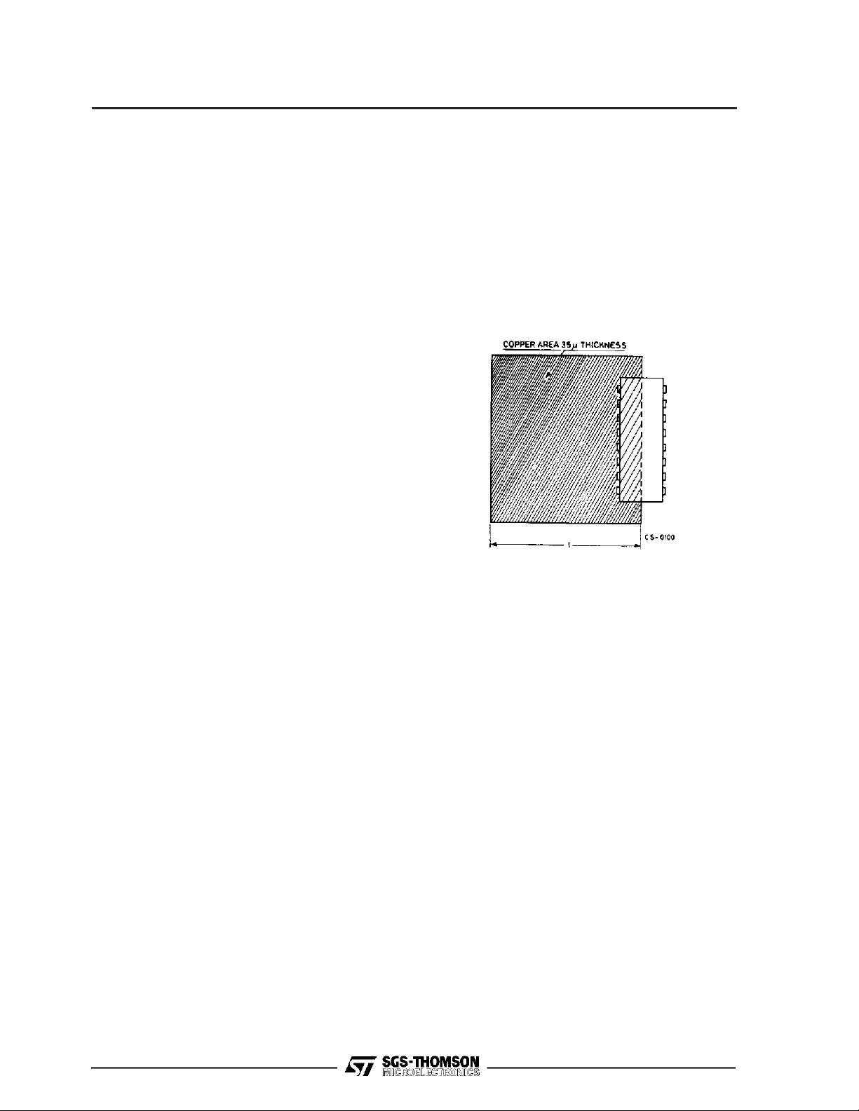
Figure21 showsa PC board copper area used as
a heatsink(I = 65 mm).
The thermal resistancejunction-ambientis 35°C.
Figure21.Exampleofheatsinkusing PC board
copper(l = 65 mm)
8/10

POWERDIPPACKAGE MECHANICAL DATA
TDA1904
DIM.
MIN. TYP. MAX. MIN. TYP. MAX.
a1 0.51 0.020
B 0.85 1.40 0.033 0.055
b 0.50 0.020
b1 0.38 0.50 0.015 0.020
D 20.0 0.787
E 8.80 0.346
e 2.54 0.100
e3 17.78 0.700
F 7.10 0.280
I 5.10 0.201
L 3.30 0.130
Z 1.27 0.050
mm inch
9/10

TDA1904
Information furnished is believed to be accurate and reliable. However, SGS-THOMSON Microelectronics assumes no responsibility for the
consequences of use of such information nor for any infringement of patents or other rights of third parties which may result from itsuse. No
license isgrantedby implication or otherwiseunder anypatent or patent rightsofSGS-THOMSON Microelectronics.Specifications mentioned
in this publication are subject to change without notice. This publication supersedes and replaces all information previously supplied.
SGS-THOMSONMicroelectronics products arenot authorizedforuseascriticalcomponentsin life supportdevices orsystems without express
written approval of SGS-THOMSONMicroelectronics.
1994 SGS-THOMSON Microelectronics-AllRightsReserved
SGS-THOMSON Microelectronics GROUP OF COMPANIES
Australia - Brazil - France - Germany - Hong Kong- Italy- Japan - Korea- Malaysia - Malta - Morocco - The Netherlands- Singapore-
Spain - Sweden - Switzerland -Taiwan- Thaliand - UnitedKingdom - U.S.A.
10/10
 Loading...