

■
NOISE GATED HORIZONTAL SYNC SEPARATOR
■
NOISE GATED VER T ICA L SY NC SE PARATOR
■
HORIZONTAL OSCILLATOR WITH FREQUENCY RANGE LIMITER
■
PHASE COMPARATOR BETWEEN SYNC
PULSES AND OSC ILLATOR P ULSE S (PLL)
■
PHASE COMPARATOR BETWEEN FLYBACK
PULSES AND OSC ILLATOR P ULSE S (PLL)
■
LOOP GAIN AND TIME CONSTANT SWITCHING ( VCR)
■
COMPOSITE BLANKING AND KEY PULSE
GENERATOR
■
PROTECTION CIRCUITS
■
OUTPU T S TAGES WI TH HI GH CURRENT CAPABILITY
TDA1180P
TV HORIZONTAL PROCESSOR
DIP16
(Plastic Package)
ORDER CODE : TDA1180P
DESCRIPTION
The TDA1 180P is a horizont al processor cir cuit for
b.w. and colour monitors. It is a monolithic integrated circuit encapsulated in 16-lead dual in-line
plastic package.
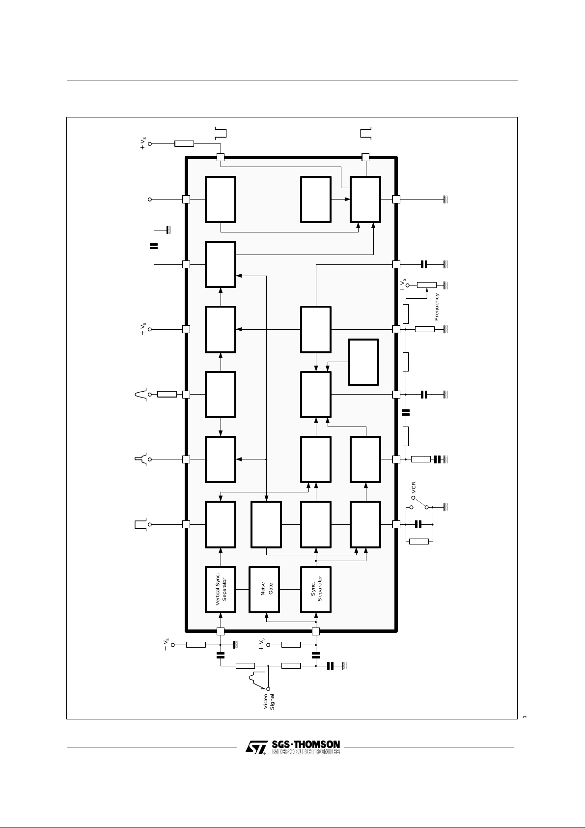
PIN CONNECTIONS
SUPPLY VOLTAGE
NEGATIVE OUTPUT
POSITIVE OUTPUT
PROTECTION CIRCUIT INPUT
PHASE SHIFTER FILTER
FLYBACK INPUT
KEY AND BLANKING PULSE OUTPUT
SYNC. SEPARATOR INPUT
1
2
3
4
5
6
7
8
16
15
14
13
12
11
10
GROUND
OSCILLATOR CONTROL CURRENT
OSCILLATOR
CONTROL CURRENT OUTPUT
TIME CONSTANT SWITCH
COINCIDENCE DETECTOR
VERTICAL SYNC. OUTPUT
9
VERTICAL SYNC. SEPARATOR INPUT
May 1993
1180P-01.EPS
1/12
TDA1180P
BLOCK DIAGRAM
S
V
2
Switch
Protection
and
Phase Shifter
Pulse Shaper
Under
Voltage
Protection
3
161415131211
Stage
Output
S
V
S
V
Phase
Flyback)
(Oscillator
Comparator
Pulse Shaper
and Blanking
Composite Key
Pulse Generator
1076154
Output Stage
Vertical Sync.
Separator
Vertical Sync.
Oscillator
Limiter
Voltage
Phase
Comparator
(Oscillator Sync .)
Blanking
Vertical Sync.
Gate
Pulse
Shaper
Gate
Noise
Sync.
Sync.
Separator
and Control
Time Constant
Current Switch
Detector
Coincidence
Frequency
VCR
2/12
S
V
9
S
V
Video
Signal
8
1180P-02.EPS

TDA1180P
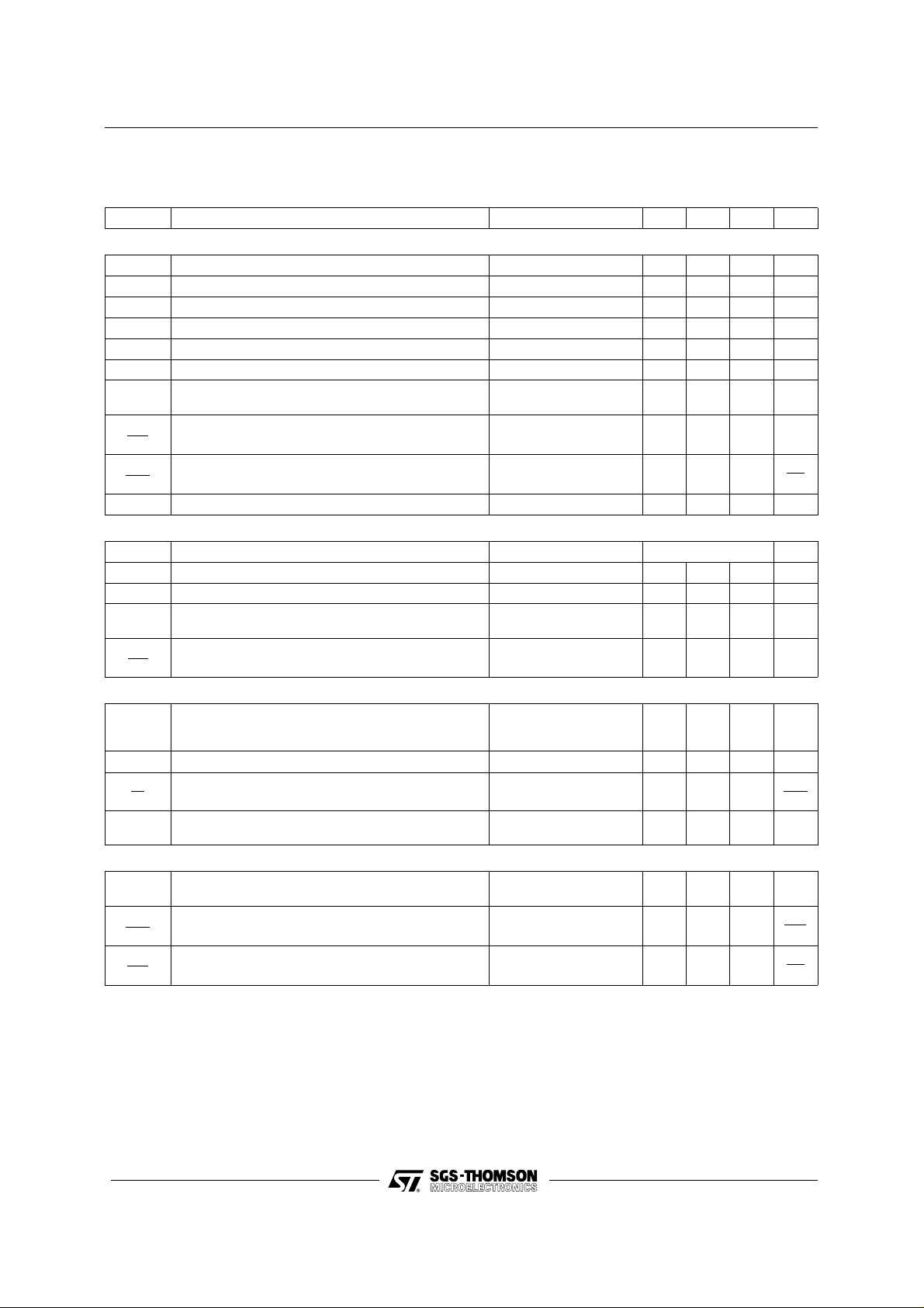
ABSOL UTE MAX IM UM RAT INGS
Symbol Parameter Value Unit
V
V
V
V
V
V
I
P
T
stg
THERMAL DATA
Supply voltage (Pin 1) 15 V
S
Voltage at Pin 2 18 V
2
Voltage at Pin 4 V
4
Voltage at Pin 8 - 6 , V
8
Voltage at Pin 9 ± 6V
9
Voltage at Pin 11 V
11
I
Pin 2 peak current 1 A
2
Pin 3 peak current 0.5 A
I
3
I
Pin 6 current 30 mA
6
Pin 7 current 20 mA
I
7
Pin 10 current 30 mA
10
Total power dissipation at Tamb ≤ 70oC1W
tot
S
S
S
, TjStorage and junction temperature - 40 , + 150
V
o
C
1180P-01.TBL
Symbol Parameter Value Unit
R
th (j-a)
Thermal Resistance Junction-Ambient Max 80
ELECTRICAL CHARACTERISTICS
(refer to the test circuit, V
Symbol Parameter Test conditions Min. Typ. Max. Unit
V
V
HORIZONTAL SYNC. SEPARATOR
V
VERTICAL SYNC. SEPARATOR
V
V
R
t
t
Supply voltage range 9.5 12 13.2 V
S
Supply current I3 = 0 42 52 mA
I
S
Supply voltage at which the output pulses
S
(at pin 2 and 3) are switched off
Peak to peak input signal 1 3 6 V
V
I
Input switching voltage I8 = 80 µA 1.5 V
8
Input switching current V8 = 1.4V 10 µA
I
8
Leakage current V8 = -5V 1 µA
I
8
Peak to Peak Input Signal 1 3 6 V
V
I
Input Switching Voltage I9= 80µA 1.5 V
9
Input Switching Current V9 = 1.4V 5 µA
I
9
Leakage Current V9 = -5V 1 µA
I
9
Vertical Sync. Pulse Output Voltage No Load Pin10 11 V
10
Output Resistance 10 kΩ
10
Delay between Leading Edge of Input and Output
LV
Signals
Delay between Trailing Edge of Input and Output
LV
Signals
t
Vertical Sync Pulse Duration 190 µs
V
= 12V, TA = 25oC, unless otherwise specified)
S
4V
17 µs
50 µs
o
C/W
1180P-02.TBL
1180P-03.TBL
3/12

TDA1180P
ELECTRICAL CHARACT E RISTICS (continued)
(refer to the test circuit, V
Symbol Parameter Test conditions Min. Typ. Max. Unit
PROTECTION CIRCUIT
V
R
FLYBACK PULSE
V
V
OUTPUT PULSE
V
R
COMPOSITE BLANKING AND KEY PULSE
V
V
R
t
t
INTERNAL GATING PULSE
COINCIDENCE DETECTOR
V
I
VCR SWITCH
V
- I
I
TIME CONSTANT SWITCH
V
R
Input Voltage for Switching off the Output Pulses Output Pulses OFF
4
Input Resistance 200 kΩ
4
Input Current 5 µA
I
4
Input Threshold Voltage of Blanking Generator 1.8 V
6
Input Threshold Voltage of Phase Comparator 7.6 V
6
Input Switching Current V6 ≥ 1.7V 0.45 mA
I
6
Peak-to-Peak Output Voltage I3 = 150 mApp 10 V
3
Output Current V3 = 5V 500 mA
I
3
Output Resistance At Leading Edge of
3
Output Pulse Duration 20 22 26 µs
t
p
Key Pulse Output Peak Voltage 9 11 V
7k
Blanking Pulse Output Voltage 4.2 4.5 4.8 V
7B
Output Resistance 100 Ω
7
Phase Relation Between Trailing Edge of Key
sk
Pulse and Middle of Sync. Input Pulse
Key Pulse Duration 3.5 3.8 µs
t
k
Delay between Flyback Pulse and Blanking Pulse V6 = 1.7V 0.2 µs
fb
Gating Pulse Duration 7.5 µs
t
g
t Phase Relation between Middle of Sync. Pulse
and Trailing and Leading Edge of Gating Pulse
Output Voltage With Coincidence
11
Peak Output Current 0.5 mA
11
Input Voltage 0 to 4 or 8.5 to 12 V
11
Output Current 35 µA
11
Output Current 0.4 mA
11
Output Voltage 3V
12
Output Resistance 4.5V < V11 < 8V
12
= 12V, TA = 25oC, unless otherwise specified)
S
Output Pulses ON 1
output pulse
At Training Edge of
Output Pulse
Without Coincidence
> 8.5V or V11 < 4V
V
11
0.5 V
3
20
2.7 µs
3.75 µs
6.8
4
100
40
Ω
Ω
V
V
Ω
kΩ
1180P-04.TBL
4/12
TDA1180P
ELECTRICAL CHARACTERISTICS (continued)
(refer to the test circuit, V
Symbol Parameter Test conditions Min. Typ. Max. Unit
OSCILLATOR
V
V
I
I
V
I
f
Low Level Threshold Voltage 5.4 V
14
High Level Threshold Voltage 8.2 V
14
Charge Current 0.6 mA
14
Discharge Current 0.3 mA
14
Current Source Supply Voltage 3 V
15
Current Source Supply Current 0.3 mA
15
Free Running Frequency 15625 Hz
O
= 12V, TA = 25oC, unless otherwise specified)
S
∆f
f
∆f
∆I
∆f
Adjustment Range ± 10 %
O
O
Frequency Control Sensitivity 52 Hz
O
15
Frequency Change when VS Drops to 4V ± 10 %
O
OSCILLA TOR-FLYBACK PULSE PHASE COMP ARATOR
V
∆t
∆t
Control Voltage Range 9.4 to 8.2 V
5
Peak Control Current -0.6 +0.6 mA
I
5
Input Current (blocked Phase Detector) 5 µA
I
5
Permissible Delay between Output Pulse Leading
t
D
Edge and Flyback Pulse Leading Edge
Static Control Error 0.2 %
D
SYNC PULSE-OSCILLATOR PHASE COMPARATOR
V
I
∆f
Control Voltage Range 4.6
13
Control Peak Current +2 -2.2 -2 mA
13
Phase Lock Loop Gain 2 kHz
∆t
f Catching and Holding Range ±
OVERALL PHASE RELATIONSHIP
t
∆V
∆t
∆I
∆t
Phase Relation between Middle of Flyback Pulse
O
and Middle of Sync. Pulse
Adjustment Sensitivity 65 mV
5
O
Adjustment Sensitivity 16 µA
5
O
tp - t
to
1.4
700
2.2 µs
µA
f
µs
V
µs
Hz
µs
µs
1180P-05.TBL
5/12
TDA1180P
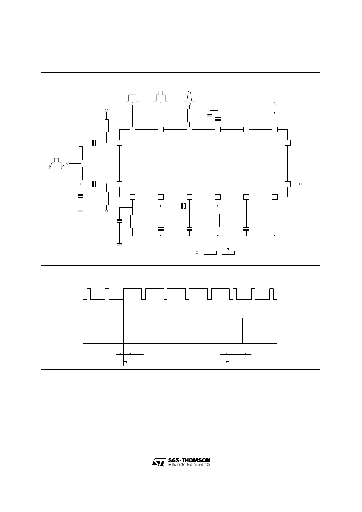
TEST CIRCUIT
Video Signal
Input
C2
100pF
R3
2.2M
C1 470nF
R1
2.2k
Ω
R2
2.7k
Ω
C3 220nF
Ω
+V
S
Vert. Sync.
Output
+V
S
R4
1.5M
C4
100nF
Sandcastle
Output
Flyback
Input (100V)
R8
47k
Ω
10
9
765
C8
220nF
+V
S
14
2
TDA1180P
8
11
Ω
R5
820k
12 13 15 14 16
R7 R9
1.2k
R6
3.6k
Ω
C5
680nF
Ω
C6
C7
10nF
4.7
Ω
100k
F
µ
Ω
R10
10k
Ω
R11
82k
Ω
C9
4.3nF
Output
3
Pulse
Figure 1 : Vertical Sync. Output Pulse
tt
LV TV
S
R12 P2
22k
Ω
22k
Frequency
Ω
1180P-03.EPS
1180P-04.EPS
+V
t
V
6/12
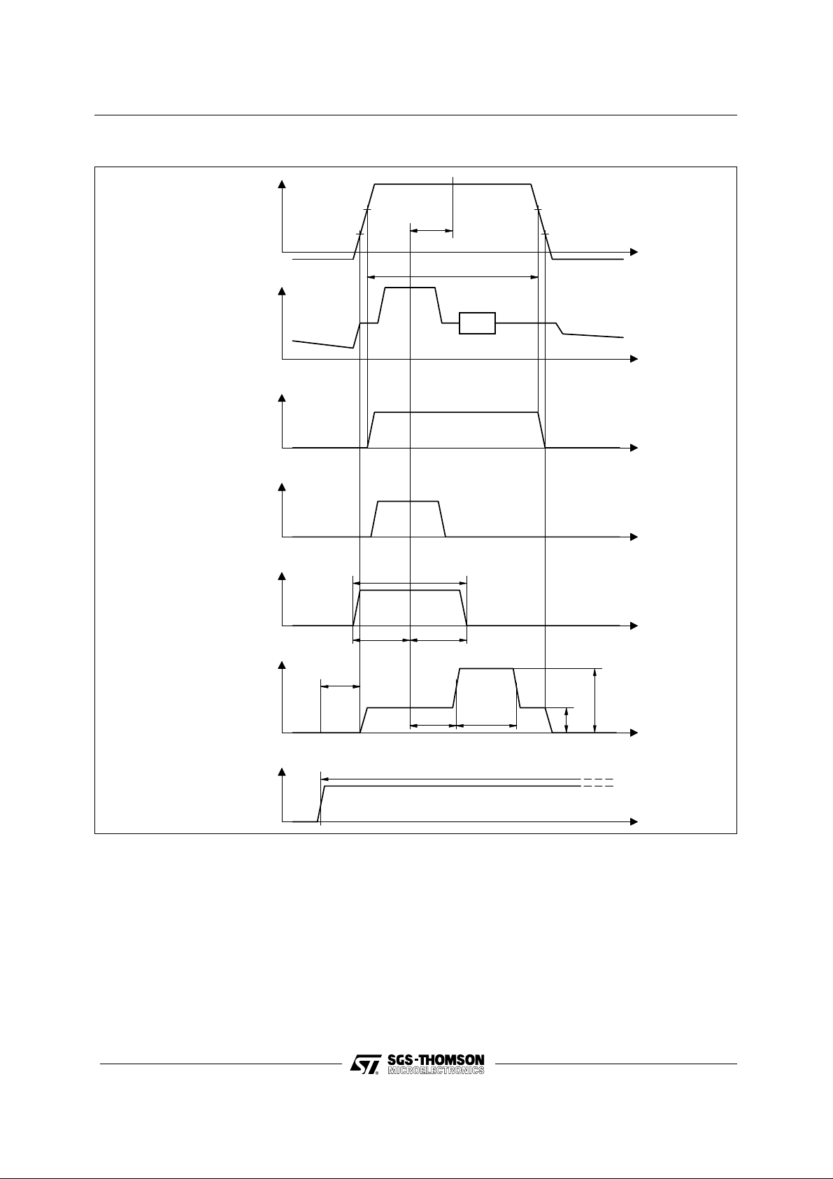
Figure 2 : Relation Ship of Main Waveform Phases
TDA1180P
Flyback
Input Pulse
Video Input
Signal
Phase Comparator
Driving Pulse
Separated
Sync. Pulse
Gate Pulse
t
o
t
f
t
g
Sandcastle
Output Pulse
Output Pulse
Pin 3
tt
t
d
V
t
SK
t
K
t
p
7K
V
7B
1180P-05.EPS
7/12

TDA1180P
Figure 3 : Free Running Frequency vers us
Supply Voltage
f (kHz)
O
16
15.625
15.5
V (V)
15
0 2 4 6 8 10 12 14 16
S
APPLICATION INFORMATION
Pin 1 - Positive supply
The operating supply voltage of the device ranges
from 10V to 13.2V
Pin 2 and 3 - Output
The outputs of TDA1180P are suitable for driving
transistor output stages, they deliver positive pulse
at Pin 3 and negative pulse at Pin 2.
The negative pulse is used for direct driving of the
output stage, while positive pulse is useful when a
driver stage is required.
The rise and fall times of the output pulses are
about 150 ns so that interference due to radiation
are avoided.
Furthermore the output stages are internally protected against short circuit.
Pin 4 - Protection circuit input
By connecting Pin 4 of the IC to earth the output
pulses at Pin 2 and 3 are shut off ; this function has
been introduced to produced to protect the final
stages from overloads.
The same pulses are also shut of f when the s upply
voltage falls below 4V.
Pin 5 - Phase shifter filter
T o com pensate for the delay introduced by the line
final stages, the flyback pulses to Pin 6 and the
oscillator waveform are compared in the oscillator flyback pulse phase comparator .
The result of the comparison is a control current
which, after it has been filtered by the external
capacitor connected to Pin 5, is sent to a phase
shifter which adequately regulates the phase of the
output pulses.
Figure 4 : Loop Gain
f (kHz)
O
1
0
-1
-0.8 -0.6 -0.4 -0.2 0 0.2 0.4 0.6 0.8
1180P-06.EPS
The maximum phase shift allowed is: t
= tp - t
d
where tf is the flyback pulse duration.
Pin 5 has high input and output resistance (c urrent
generator).
Pin 6 - Flyback input
The flyback pulse drives the high impedance input
through a resistor in order to limit the input current
to suitable maximum values.
The flyback input pulses are processed by a double
threshold circuit; this generates the blanking pulses
by sensing low level flyback voltage a nd the pulses
to drive the phase comparator by sensing high level
flyback voltage, therefore phase jitter caused by
ringing normally associated with t he fly back pulse,
is avoided.
Pin 7 - Key and blankin g pulse o ut put
The key pulse for taking out the burst from the
chrominance signal is generated from the oscillat or
ramp and has therefore a f ixed ph ase position with
respect to the sync.
The key pulse is then added internally to the blanking pulse obtained by correctly form in g the flyback
pulse present at Pin 6.
The sum of the two signals (sandcastle pulse) is
available on low impedance at output Pin 7.
Pin 8 and 9 - Sync separators inputs
The video signal is applied by means of two distinct
biasing networks to pins 8 and 9 of the IC and
therefore to the respective vertical and horizontal
sync separators.
The latter take the sync pulses out of the video
signal and make them available to the rest of the
circuit for further process ing.
ϕ
(µ s)
1180P-07.EPS
f
8/12

TDA1180P
Pin 10 - Verti cal sync outp u t
The vertical sync pulse, obtained by internal integration of the synchronizing signal, is available at
this pin.
The output impedance is typically 10kΩ and the
lowest amplitude without load is 11V.
Pin 1 1 - Coincidence det ecto r
From the oscillator waveform a gate pulse 7 µs
wide is taken whose phase position is centered on
the horizontal sy nchronism.
The gate pulse not only controls a logic block which
permits the sync to reach the oscillat or-sync phase
comparator only for as long as its duration, but als o
allows the latching and de-latching conditions of
the oscillator to be established.This function is
obtained by a coincidence detector which compares the phase of the gate pulses with that of the
sync.
When the two signals are not accurately aligned in
time it means that the oscillator is not synchronized.
In this case the detector acts on the logic block to
eliminate its filtering ef fect and on the time constant
switching block to establish a high impedance on
Pin 12 (small time constant of low-pass filter).
This latter block also acts on the oscillator-sync
phase detector to increas e its s ensitivity and with it
the loop gain of the synchronizing system.
In this conditions the phase lock has low noise
immunity (wide equivalent noise bandwidth) and
rapid pull-in time which allows fair ly s hort synchronization times.
Once locking has taken place the coincidence detector enables the logic block, caus es a low impedance on Pin 12 and reduces the sensitivity of the
phase comparator.
In these conditions the phase lock has high noise
immunity ( narrow equivalent noise bandwidth) due
to the complete elimination of interference which
occurs during the scanning period and the greater
inertia with which the oscillator can change its
frequency.
To optimize the behaviour of the IC if a video
recorder is used, the state of the detector can be
forced by connecting P in 1 1 to earth or to + V
. The
S
characteristics of the phase lock thus correspond
to the lack of synchronization.
Pin 12 - Time constant switch, (see Pin 11)
Pin 13 - Control current output
The oscillator is synchronized by comparing the
phase of its waveform with that of the sync pulses
in the oscillator-sync phase comparator and sending its output current I13 (proportional to the phase
difference between the t wo signals) to Pin 15 of t he
oscillator after it has been filtered properly with an
external low-pass circuit.
The time constant of the filter can be switched
between two values according to the impedance
presented by Pin 12.
The voltage limiter at the output of the phase
comparator limits the voltage excursion on Pin 13
and therefore the frequency range in which the
oscillator remains held-in.
The output resistance of Pin 13 is:
● low when V13 > 4.3 or V13 < 1.6V
● high when 1.6V < V13 < 4.3V
To prevent the vertical sync from reaching the
oscillator-sync phase comparator along with the
horizontal sync,a signal which inhibits the phase
detector during the vertical interval is taken from
the vertical output stage; inhibition remain even if
the video signal is not present.
The free running frequenc of the os cillator is determined by the values of the capacitor and of the
resistor connected to Pins 14 and 15 respectively.
To generate the line frequency output pulses, two
theresholds are fixed along the fall ramp of the
triangular waveform of the oscillator.
Pin14 - Oscillato r (see Pin 13)
Pin 15 - Oscillator cont rol curr ent input (see
Pin 13)
Pin 16 - Ground
9/12

TDA1180P
Figure 5 : Application Circuit for Large Screen Black & White and Colour TV
R3
2.2M
C1 470nF
R1
Ω
2.2k
Vert. Sync.
+V
Ω
S
Output
Sandcastle
Output
Flyback
Input (100V)
R8
47k
Ω
10
9
765
C8
220nF
R13
220k
+V
S
Phase
P1
Ω
220k
Ω
14
2
TDA1180P
C2
100pF
R2
2.7k
Ω
C3 220nF
8
R4
11
1.5M
Ω
+V
S
C4
100nF
R5
820k
12 13 15 14 16
R7 R9
1.2k
Ω
R6
3.6k
C5
680nF
Ω
Ω
C7
10nF
100k
F
+V
S
Ω
R10
Ω
10k
R12 P2
22kΩ22k
R11
Ω
82k
Ω
C6
4.7
µ
C9
4.3nF
Frequency
R14
3
560
Ω
Video Signal
Input
Figure 6 : P.C. Board and Component Layout for the Circuit in Figure 6 (1:1 scale)
C10
120
6.8nF
Q1
+32V
220
Ω
F
10
µ
BU406D
Ω
BC440
1180P-08.EPS
10/12
VIDEO SIGNAL INPUT
SANDCASTLE OUTPUT
FLYBACK INPUT (100V)
V
VERTICAL SYNC. OUTPUT
OUTPUT PULSE
P1
R1
S
C1
C3
R4
TDA1180P
R14
R3
R7
R8
R2
C2
R12
R13
C8
C10
C9
R10
R11
R6
Q1
R5
C4
C6
R9
P2
C5C7
1180P-09.EPS
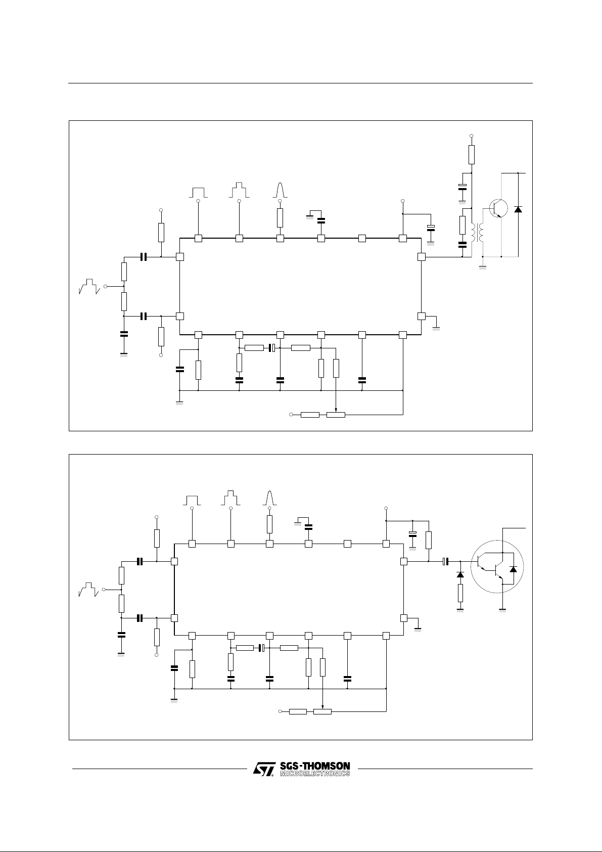
Figure 7 : Application Circuit for Small Screen b.w. TV
Sandcastle
Output
R8
47k
Ω
Flyback
Input (100V)
R3
2.2M
C1 470nF
R1
2.2k
Ω
Vert. Sync.
+V
Ω
S
Output
10
9
765
TDA1180P
C2
100pF
R2
2.7kΩ
C3 220nF
8
R4
1.5M
+V
S
C4
100nF
11
Ω
R5
820k
12 13 15 14 16
R7 R9
Ω
R6
3.6k
C5
680nF
1.2k
Ω
Ω
C7
10nF
C6
4.7µF
100k
R10
10k
Ω
Video Signal
Input
TDA1180P
+10.8V
15
Ω
+V
S
C8
220nF
R11
Ω
82k
Ω
C9
4.3nF
100µF
14
10µF
68Ω
15nF
2
3
BU407D
R12 P2
+V
S
22kΩ22k
Figure 8 : Application Circuit for Darlington Output Stage
Sandcastle
Output
Flyback
Input (100V)
R8
47k
Ω
C8
220nF
R3
2.2M
C1 470nF
R1
2.2k
Ω
Vert. Sync.
+V
Ω
S
Output
10
9
765
TDA1180P
C2
100pF
R2
2.7k
Ω
C3 220nF
8
R4
11
Ω
1.5M
+V
S
C4
100nF
R5
820k
12 13 15 14 16
R7 R9
1.2k
Ω
R6
3.6k
C5
680nF
Ω
Ω
C7
10nF
100k
C6
4.7
Ω
µ
F
R10
10k
Ω
Video Signal
Input
R11
82k
Ω
Frequency
+V
S
µ
F
100
14
Ω
C9
4.3nF
82
Ω
2
3
4.7µF
33
Ω
BU806 or
BU807
1180P-10.EPS
+V
S
R12 P 2
Ω
22k
22k
Ω
Frequency
1180P-11.EPS
11/12

TDA1180P
PACKA G E MECHANICAL DATA
16 PINS - PLASTIC DIP
a1
Z
b
B
e
e3
I
L
b1
E
D
16
9
F
18
Dimensions
Min. Typ. Max. Min. Typ. Max.
a1 0.51 0.020
B 0.77 1.65 0.030 0.065
b 0.5 0.020
b1 0.25 0.010
D 20 0.787
E 8.5 0.335
e 2.54 0.100
e3 17.78 0.700
F 7.1 0.280
i 5.1 0.201
L 3.3 0.130
Z 1.27 0.050
Millimeters Inches
PM-DIP16.EPS
DIP16.TBL
Information furnished is believed to be accurate and reliable. However, SGS-THOMSON Microelectronics assumes no responsibility
for the consequences of use of such information nor for any infri ngement of patents or other rights of third parties which may result
from its use. No licence is granted by implication or otherwise under any patent or patent rights of SGS-THOMSON Microelectroni cs.
Specifications mentioned in this publication are subject to change without notice. This publication supersedes and replaces all
information previously suppli ed. SGS-THOMSON Microel ectronics products are not authorized for use as critical components in life
support devices or systems without express written approval of SGS-THOMSON Microelectronics.
© 1994 SGS-THOMSON Microelectronics - All Rights Reserved
2
Purchase of I
2
C Patent. Rights to use these components in a I2C system, is granted provided that the system conforms to
I
Australia - Brazil - China - France - Germany - Hong Kong - Italy - Japan - Korea - Malaysia - Malta - Morocco
The Netherlands - Singapore - Spain - Sweden - Switzerland - Taiwan - Thailand - United Kingdom - U.S.A.
C Components of SGS-THOMSON Microelectronics, conveys a license under the Philips
2
C Standard Specifications as defined by Philips.
the I
SGS-THOMSON Microelectronics GROUP OF COMPANIES
12/12
 Loading...