

UA
SOP
TC1040
Linear Building Block – Dual Low Power Comparator and
Voltage Reference with Shutdown
Features
• Combines Two Comparators and a Voltage
Reference in a Single Package
• Optimized for SingleSupply Operation
• Small Package: 8-Pin MSOP
• Ultra Low Input Bias Current: Less than100pA
• Low Quiescent Current, Operating: 10µA(Typ.)
Shutdown Mode: 6µA(Typ.)
• Rail-to-Rail Inputs and Outputs
•OperatesDowntoV
DD
=1.8V
• Referenceand One Comparator Remain Active in
Shutdown to Provide Supervisory Functions
Applications
• Power Supply Circuits
• Battery Operated Equipment
• Consumer Products
• Replacements for Discrete Components
Device Selection Table
Part Number Package
TC1040CEUA 8-Pin MSOP -40°C to +85°C
Temperature
Range
Package Type
General Description
The TC1040 is a mixed-function device combining two
comparators and a voltage reference in a single 8-pin
package. The inverting input of Comparator A and the
non-inverting input of Comparator B are internally
connected to thereference.
This increased integration allows the user to replace
two packages, which saves space, lowers supply
current and increases system performance. The
TC1040 operates from two 1.5V alkaline cells down to
V
= 1.8V. It requires only 10µA typical of supply
DD
current, which significantly extends battery life. A low
power shutdown input (SHDN
) disables one of the
comparators, placing its outputs in a high-impedance
state. This mode saves battery power and allows
comparator outputs to share common analog lines
(multiplexing). Shutdown current is 6µA(typical).
Rail-to-rail inputs and outputs allow operation from low
supply voltages with large input and output signal
swings.
Packaged in an 8-Pin MSOP, the TC1040 is ideal for
applicationsrequiring low power leveldetection.
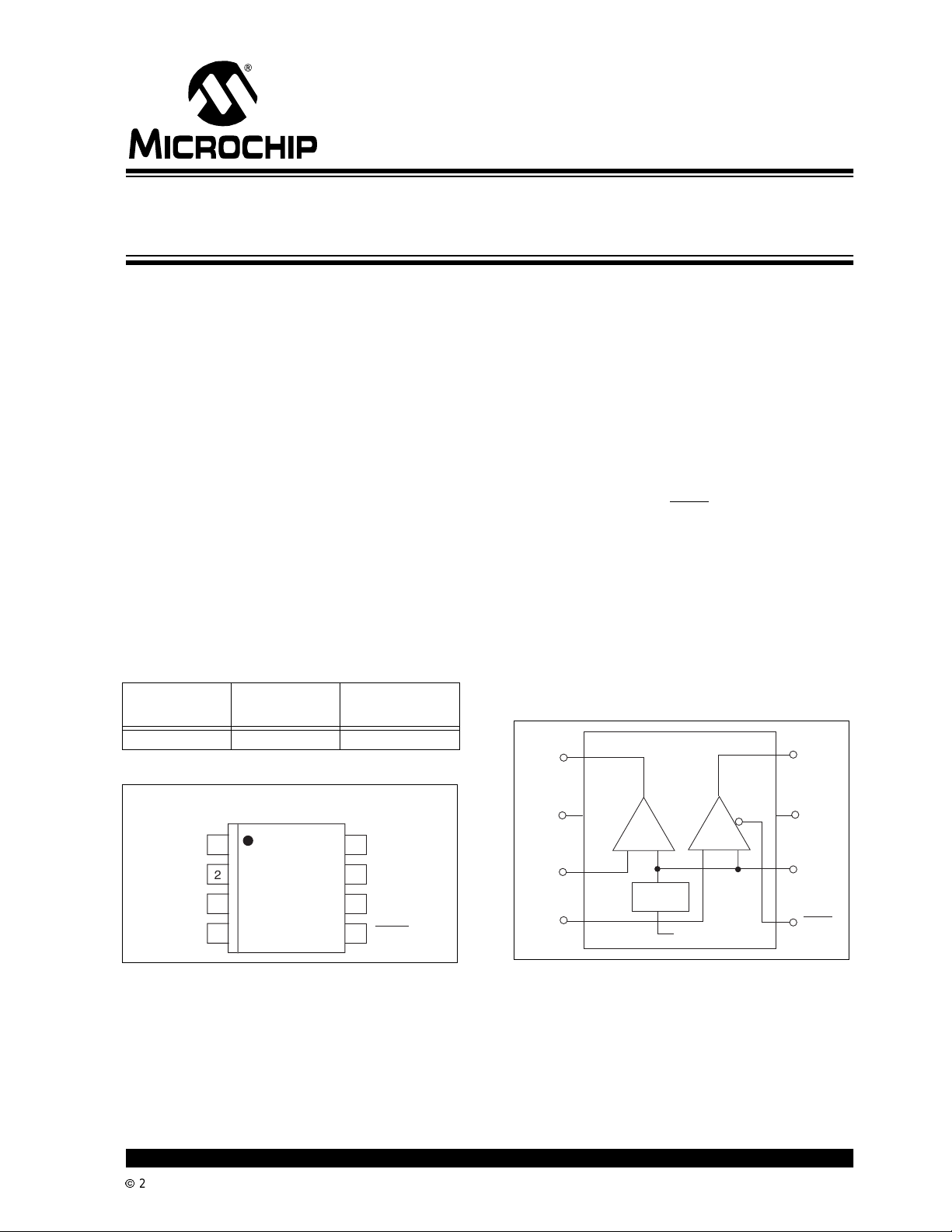
Functional Block Diagram
OUTA
1
TC1040
8
OUTB
-Pin M
OUTB
OUTA
V
SS
INA+
INB-
2002 Microchip TechnologyInc. DS21345B-page 1
TC1040CE
8
7
6
5
V
DD
REF
SHDN
V
INA+
INB-
2
SS
3
4
A
+
–
Voltage
Reference
B
–
V
SS
7
V
DD
+
6
REF
5
SHDN

TC1040
1.0 ELECTRICAL
CHARACTERISTICS
*Stresses above those listed under "Absolute Maximum
Ratings" may cause permanent damage to the device. These
are stress ratings only and functional operation of t he device
at these or any other conditions above those indicated in the
ABSOLUTE MAXIMUM RATINGS*
Supply Voltage......................................................6.0V
Voltage on Any Pin..........(V
– 0.3V) to (VDD+0.3V)
SS
operation sections of the specifications is not implied.
Exposure to Absolute Maximum Rating conditions for
extended periods may affectdevice reliability.
Junction Temperature.......................................+150°C
Operating Temperature Range.............-40°C to +85°C
StorageTemperature Range..............-55°C to +150°C
TC1040 ELECTRICAL SPECIFICATIONS
Electrical Characteristics: Typical values apply at 25°C and VDD= 3.0V. Minimum and maximum values apply for TA= -40° to
+85°C and V
Symbol Parameter Min Typ Max Units Test Conditions
V
DD
I
Q
I
SHDN
Shutdown Input
V
IH
V
IL
I
SI
Comparators
(SD) Output Resistance in Shutdown 20 — — MΩ SHDN =VSS,COMPBonly
R
OUT
(SD) Output Capacitance in Sh utdown — — 5 pF SHDN =VSS,COMPBonly
C
OUT
T
SEL
T
DESEL
V
IR
V
OS
I
B
V
OH
V
OL
PSRR Power Supply Rejection Ratio 60 — — dB TA=25°C
I
SRC
I
SINK
t
PD1
t
PD2
Voltage Reference
V
REF
I
REF(SOURCE)
I
REF(SINK)
C
L(REF)
E
VREF
e
VREF
= 1.8V to 5.5V,unless otherwise specified.
DD
Supply Voltage 1.8 — 5.5 V
SupplyCurrent Operating — 10 15 µA All outputs unloaded, SHDN =V
Supply Current, Shutdown — 0.05 0.1 µA SHDN =V
InputHighThreshold 80% V
Input Low Threshold — — 20% V
——V
DD
DD
V
SS
Shutdown Input Current — — ±100 nA
Select Time (For Valid Output) — 20 — µsec (SHDN =VIHto V
R
=10kΩ to V
L
Deselect Time — 500 — nsec (SHDN =VILto V
R
=10kΩ to V
L
)
OUT
COMPB only
SS,
)
OUT
COMPB only
SS,
Input Voltage Range VSS–0.2 — VDD+0.2 V
Input Offset Voltage -5
-5
—+5+5mV VDD=3V,TA=25°C
T
=-40°Cto85°C
A
Input Bias Current — — ±100 pA TA= 25°C, INA+, INB-= VDDto V
OutputHighVoltage VDD–0.3 — — V RL=10kΩ to V
OutputLow Voltage — — 0.3 V RL=10kΩ to V
V
=1.8Vto5V
DD
OutputSource Current 1 — — mA INA+= VDD,INB-=V
OutputShorted to V
SS
DD
SS
SS
VDD=1.8V
OutputSinkCurrent 2 — — mA INA+= VSS,INB-=V
OutputShorted to V
VDD=1.8V
DD,
DD
Response Time — 4 — µsec 100mV Overdrive, CL= 100pF
Response Time — 6 — µsec 10mV Overdrive,CL= 100pF
Reference Voltage 1.176 1.200 1.224 V
Source Current 50 — — µA
Sink Current 50 — — µA
Load Capacitance — — 100 pF
Voltage Noise — 20 — µV
100Hz to 100kHz
RMS
Noise Density — 1.0 — µV/√Hz 1kHz
DD
SS
DS21345B-page 2
2002 Microchip TechnologyInc.
2.0 PIN DESCRIPTION
The description of the pins are listed i n Table 2-1.
TABLE 2-1: P IN FUNCTION TABLE
TC1040
Pin No.
(8-Pin MSOP)
1 OUTA Comparator output.
2V
3 INA+ Non-inverting input to Comparator A.
4 INB- InvertinginputtoComparator B.
5 SHDN
6 REF Voltage reference output.
7V
8 OUTB Comparator output.
Symbol Description
SS
DD
Negative power supply.
Shutdown input.
Positive power supply.
2002 Microchip TechnologyInc. DS21345B-page 3
TC1040
3.0 DETAILED DESCRIPTION
The TC1040 i s oneof a series of v ery lowpower, linear
building block products targeted at low voltage, single
supply applications. The TC1040 minimum operating
voltage is 1.8V and typical supply current is only 10µA
(fully enabled). It combines two comparators and a
voltage reference in a single package. A shutdown
mode is incorporated for easy adaptation to system
power management schemes. During shutdown, one
comparatoris disabled (i.e., powered down with output
at a high impedance).The“stillawake”comparatorand
voltage reference can be used as a wake-up timer,
power supply monitor, LDO controller or other
continuous duty circuit function.
3.1 Comparators
The TC1040 contains t wo comparators. The comparator’s inputrange extends beyond both supply voltages
by 200mV and the outputs will swing to within several
millivolts of thesupplies,depending on theload current
being driven. The inverting input of Comparator A and
the non-inverting input of Comparator B are internally
connected to the output of the voltage reference.
The comparators exhibit a propagation delay and
supply current which are largely independent of supply
voltage. The low input bias current and offset voltage
make them suitable f or high impedance precision
applications.
Comparator B is disabled during shutdown and has a
high impedance output. Comparator COMPA remains
active.
3.2 Voltage Reference
A 2.0 percent tolerance, internally biased, 1.20V
bandgap voltage reference is included in the TC1040.
It has a push-pull output capable of sourcing and
sinking 50µA. The voltage reference remains fully
enabled during shutdown.
4.0 TYPICAL APPLICATIONS
The TC1040 lends itself to a wide variety of
applications,particularlyin battery powered systems. It
typically finds application in power management,
processor supervisory and interface circuitry.
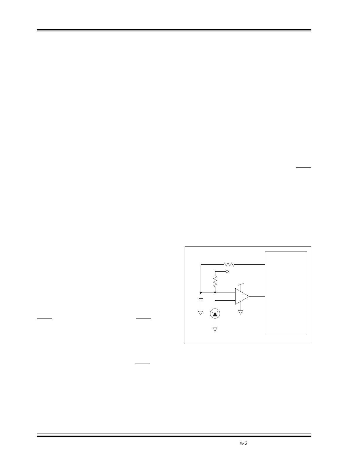
4.1 Wake-Up Timer
Many microcontrollers havea l ow-power “sleep” mode
thatsignificantly reduces their supply current. Typically,
the microcontrolleris placedin thismode via a software
instruction, and returns to a fully-enabled state upon
reception of an external signal (“wake-up”). Thewakeup signal isusually supplied by a hardware timer. Most
system applicationsdemandthatthis timer have along
duration (typically seconds or minutes), and consume
as l ittle supply current aspossible.
The circuit shown in Figure 4-1 is a wake-up timer
made from Comparator A. (Comparator A is used
because the wake-up timer must operate when SHDN
is active.) Capacitor C1 charges through R1 until a
voltage equal to V
“wake-up” is driven active. Upon wake-up, the
microcontroller resets the timer by forcing a logic low
on a dedicated,opendrainI/Oportpin. Thisdischarges
C1 through R4 (the value of R4 is chosen to limit
maximum current sunk by the I/O port pin). With a 3V
supply, the circuit as shown consumes typically 8µA
and f urnishes a nominal timer duration of25 seconds.
FIGURE 4-1: WAKE-UP TIMER
R1
5M
C
1
10µF
is reached, at which point the
R
Microcontroller
I/O*
Wake-Up
1/2
R4
V
DD
V
DD
COMPA
+
–
3.3 Shutdown Input
SHDN at VILdisablesonecomparator.TheSHDN input
cannot be allowed to float; whennotused, connect it to
V
. The disabled comparator’s output is in a high
DD
impedance state when shutdown is active. The
disabledcomparator’s inputsandoutputscan bedriven
from rail-to-rail by an external voltage when the
TC1040 is inshutdown.No latchup wi ll occurwhen the
device is driven to its enabled state when SHDN
to V
.
IH
DS21345B-page 4
is set
*Open Drain Port Pin
V
R
TC1040
2002 Microchip TechnologyInc.
TC1040
4.2 Precision Battery Monitor
Figure 4-2 is a precision battery low/battery dead
monitoring circuit. Typically, the battery low output
warns the user that a battery dead condition i s
imminent. Battery dead typically initiates a forced
shutdown to prevent operation at low internal supply
voltages(whichcan cause unstable system operation).
The circuit in Figure 4-2 uses a single TC1040, onehalf of a TC1029, and only six external r esistors.
COMPA and COMPB provide precision voltage
detection using V
R4 set the detection threshold for BATT LOW
as a reference. Resistors R2 and
R
, while
Resistors R1 and R7 set the detection threshold for
BATT FAIL. The component values shown assert
BATT LOW
at 2.2V (typical) and BATT FAIL at 2.0
(typical). Total current consumed by this circuit is
typically 22µA at 3V. Resistors R5 and R6 provide
hysteresis for comparators COMPA and COMPB,
respectively.
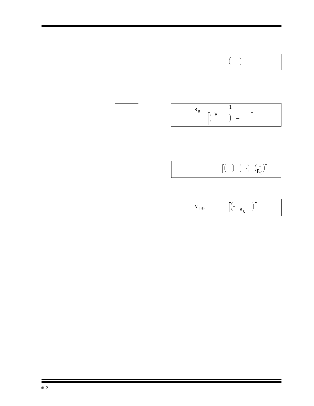
4.3 External Hysteresis (Comparator)
Hysteresis can be set externally with two resistors
using positive f eedback techniques (see Figure4-3).
The design procedure for setting external comparator
hysteresis is as follows:
1. Choose the feedback resistor R
input bias current of the comparator is at most
100pA, the current through R
100nA (i.e., 1000 times the input bias current)
and retain excellent accuracy. The current
through R
R
where VRis a stable reference voltage.
C
at the comparator’s trip point is VR/
C
2. Determinethehysteresisvoltage(V
the upper andlower thresholds.
.Sincethe
C
canbesetto
C
)between
HY
3. Calculate R
as follows:
A
EQUATION 4-1:
V
HY
=
-----------
C
V
DD
SRC
RAR
4. Choose the rising threshold voltage for V
(V
).
THR
5. Calculate R
as follows:
B
EQUATION 4-2:
R
-----------------------------------------------------------=
B
---------------------
VRRA×
6. Verify the threshold voltages with these
formulas:
V
rising:
SRC
V
THR
1
1
1
–
–
-------
-------
R
R
A
C
EQUATION 4-3:
V
V
SRC
THR
falling:
VR()RA()
------R
1
A
1
-------
++=
R
B
1
-------
R
C
EQUATION 4-4:
RAVDD×
V
THFVTHR
--------- ------------- ---
–=
R
C
2002 Microchip TechnologyInc. DS21345B-page 5
 Loading...