

SGS Thomson Microelectronics T820-800W, T820-700W, T820-600W, T830-800W, T830-700W Datasheet
...
T820-xxxW
®
FEATURES
I
■
■
■
■
■
=8A
TRMS
V
DRM=VRRM
= 600V to 800V
EXCELLENT SWITCHING PERFORMANCES
INSULATING VOLTAGE = 1500V
(RMS)
U.L. RECOGNIZED : E81734
DESCRIPTION
TheT820/830Wtriacsusehighperformanceglass
passivated chip technology, housed in a fully
molded plastic ISOWATT220AB package.
TM
The SNUBBERLESS
concept offers suppression of R-C network, and is suitable for applications such as phase control and static switch on
inductive and resistive loads.
T830-xxxW
SNUBBERLESS TRIAC
A
2
A
1
G
ISOWATT220AB
(Plastic)
A1
G
A2
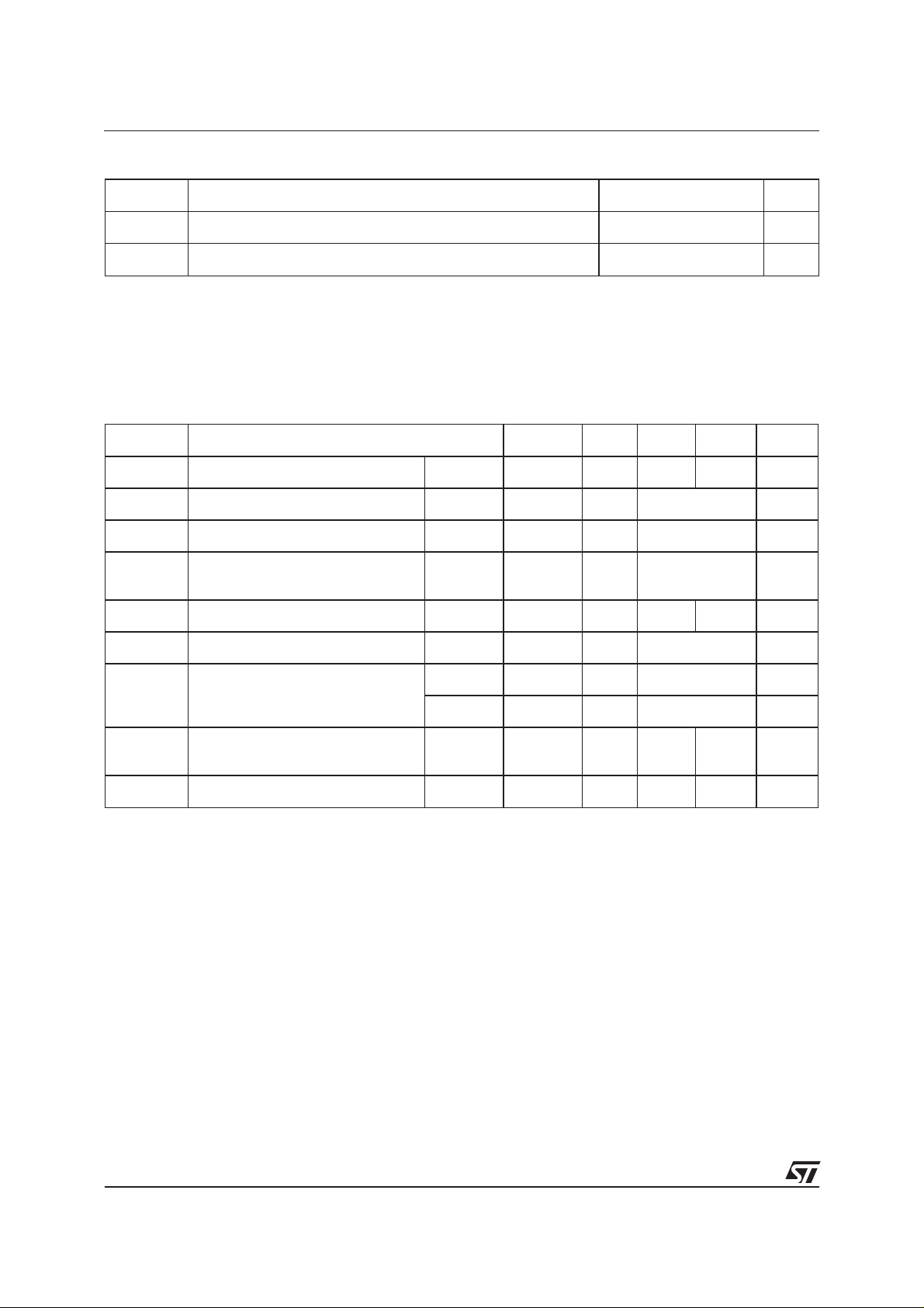
ABSOLUTE RATINGS (limiting values)
Symbol Parameter Value Unit
I
T(RMS)
RMS on-state current
Tc= 95°C 8 A
(360° conduction angle)
I
TSM
Non repetitive surge peak on-state current
initial = 25°C )
(T
j
tp = 16.7 ms
(1 cycle, 60 Hz)
tp=10ms
88 A
100
(1/2 cycle, 50 Hz)
2
t
I
dI/dt
2
I
t Value (half-cycle, 50 Hz)
Critical rate of rise of on-state current
Gate supply : I
= 500 mA dIG/dt=1A/µs.
G
tp=10ms 50 A
Repetitive
20 A/µs
F=50Hz
Non Repetitive 100
T
stg
T
j
Tl
Storage temperature range
Operating junction temperature range
Maximum lead temperature for soldering during 10s at 4.5 mm
-40to+150
-40to+125
260 °C
from case
Symbol Parameter
T820 / T830-xxxW
600 700 800
2
°C
Unit
s
V
DRM
V
RRM
September 2001 - Ed: 1A
Repetitive peak off-state voltage
= 125°C
T
j
600 700 800 V
1/5
T820-xxxW / T830-xxxW
THERMAL RESISTANCES
Symbol Parameter Value Unit
Rth(j-a)
Rth(j-c)
Junction to ambient
Junction to case for A.C (360° conduction angle)
50 °C/W
3.1 °C/W
GATE CHARACTERISTICS (maximum values)
P
=1W PGM=10W(tp=20µs) IGM=4A(tp=20µs
G (AV)
ELECTRICAL CHARACTERISTICS
Symbol Test Conditions Quadrant T820 T830 Unit
I
GT
V
GT
V
GD
tgt
*
I
H
*
V
TM
VD=12V (DC) RL=33Ω
VD=12V (DC) RL=33Ω
VD=V
DRMRL
V
D=VDRMIG
/dt= 3Aµs
dl
G
I
= 100mA Gate open
T
I
= 11A tp= 380µs
TM
=3.3kΩ
=500mA
Tj= 25°C I-II-III MAX 20 30 mA
Tj= 25°C I-II-III MAX 1.5 V
Tj= 125°C I-II-III MIN 0.2 V
Tj= 25°C I-II-III TYP 2 µs
Tj= 25°C MAX 35 50
Tj= 25°C MAX 1.5 V
I
DRM
I
RRM
VDRM rated
rated
V
RRM
Tj= 25°C MAX 10 µA
Tj= 125°C MAX 2 mA
dV/dt *
(dV/dt)c *
* For either polarity of electrode A2 voltage with reference to electrode A1.
Note : Inusualapplicationswhere (dI/dt)c is below 4.5 A/ms, the (dV/dt)c is always lower than 10V/µs, and, therefore, it is unnecessary to use
a snuber R-C network accross T820W / T830W triacs.
Linear slope up to
=67%V
V
D
DRM
Gate open
(dI/dt)c = 4.5 A/ms (see note)
Tj= 125°C MIN 200 300 V/µs
Tj= 125°C MIN 10 20 V/µs
2/5
 Loading...