

N - CHANNEL200V - 0.030Ω - 60 A - Max247
FAST POWER MOS TRANSISTOR
TYPE V
DSS
ST Y60NA20 200 V < 0.032 Ω 60 A
R
DS(on)
I
D
STY60NA20
PRELIMINARY DATA
■ TYPICALR
■ EFFICIENTANDRELIABLE MOUNTING
DS(on)
= 0.030Ω
THROUGH CLIP
■ ± 30V GATETO SOURCEVOLTAGERATING
■ REPETITIVEAVALANCHETESTED
■ LOW INTRINSICCAPACITANCE
■ 100%AVALANCHE TESTED
■ GATECHARGE MINIMIZED
■ REDUCEDTHRESHOLD VOLTAGESPREAD
DESCRIPTION
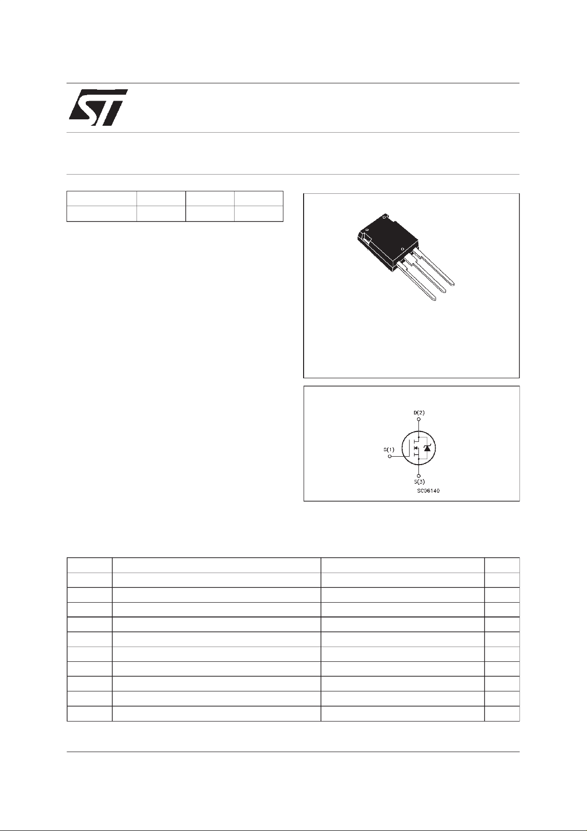
The M ax 247TMpackage is a new high volum e
power package exibiting the same foot print as t h e
indus try standard TO-247, but designe d t o
accomodate much larger si licon c h ips , normally
suppl ied in bigger p ac kages suc h as T O -264. Th e
increased die ca pacity m akes the device ideal to
reduce com ponent cou nt in multiple parallele d
desig ns and save boar d s pace with respect to
larger packa ges.
APPLICATIONS
■ HIGHCURRENT, HIGHSPEED SWITCHING
■ SWITCHMODE POWERSUPPLIES(SMPS)
■ DC-AC CONVERTERS FORWELDING
EQUIPMENTANDUNINTERRUPTIBLE
POWERSUPPLIES (UPS)
3
2
1
Max247
TM
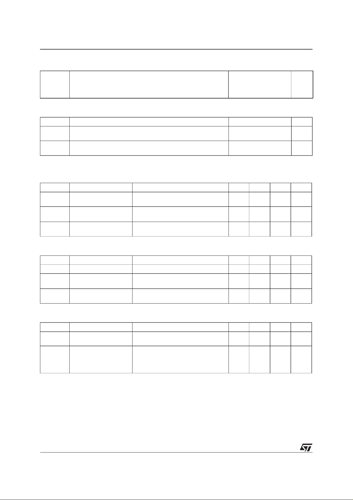
INTERNAL SCHEMATIC DIAGRAM
ABSOLUTE MAXIMUM RATINGS
Symb o l Parame t er Val u e Uni t
V
V
DGR
V
I
DM
P
T
(•) Pulse width limited by safe operating area
August 1998
Drain-s ource Voltage (VGS= 0 ) 200 V
DS
Drain- gate Volt age ( RGS=20kΩ)
Gate-source Volt age ± 30 V
GS
I
Drain Cur rent (cont in uous ) at Tc=25oC60A
D
I
Drain Cur rent (cont in uous ) at Tc=100oC40A
D
200 V
(•) Drain Current (pulsed) 240 A
Total Dissipation at Tc=25oC 300 W
tot
Derat ing F actor 2.4 W/
Stora ge Temper at u re -65 to 150
stg
T
Max. Op er at i ng Junc t ion Temper a t ur e 150
j
o
C
o
C
o
C
1/4
STY60NA20
THERMAL DATA
R
thj-case
R
thj- amb
R
thc-sin k
AVALANCHE CHARACTERISTICS
Symb o l Para met er Max Value Uni t
I
AR
E
Ther mal Resistance Junct ion-cas e Max
Ther mal Resistance Junct ion-ambi ent Max
Ther mal Resistance Case-Heatsink Typ
with Conductive Grease
Avalanche Current , Rep et it ive or Not -R epe t it ive
(pulse width lim it e d by T
Singl e Pulse Ava lanche Energy
AS
(starti ng T
=25oC, ID=IAR,VDD=50V)
j
max)
j
0.42
40
0.05
60 A
3000 mJ
o
C/W
o
C/W
ELECTRICAL CHARACTERISTICS (T
=25oC unlessotherwisespecified)
case
OFF
Symbol Parameter Test Condition s Min. Typ. Max. Unit
V
(BR)DSS
Drain-source
= 250 µAV
I
D
GS
=0
200 V
Break dow n Voltage
I
I
DSS
GSS
Zero Gate Voltage
Drain Current (V
GS
Gat e- bod y Le akage
Current (V
DS
=0)
=0)
V
=MaxRating
DS
= Max Rating Tc=100oC
V
DS
= ± 30 V
V
GS
1
10
± 100 nA
ON (∗)
Symbol Parameter Test Condition s Min. Typ. Max. Unit
V
GS(th )
R
DS(on)
Gat e Thr e shold Volt a ge
St at i c Drain -s ource O n
V
DS=VGSID
=250µA
VGS=10V ID= 30A 0.03 0.032 Ω
234V
Resistance
I
D(on)
On State Drain Current VDS>I
D(on)xRDS(on)max
60 A
VGS=10V
DYNAMIC
Symbol Parameter Test Condition s Min. Typ. Max. Unit
g
(∗)Forward
fs
Tr ansc on ductance
C
C
C
Input Capacitan c e
iss
Out put Ca pac itanc e
oss
Reverse Tr ansfer
rss
Capaci ta nc e
VDS>I
D(on)xRDS(on)maxID
=30A 20 S
VDS=25V f=1MHz VGS= 0 6000
1400
500
8000
1900
700
µA
µA
pF
pF
pF
2/4

STY60NA20
ELECTRICAL CHARACTERISTICS (continued)
SWITCHINGON
Symbol Parameter Test Condition s Min. Typ. Max. Unit
t
d(on)
Q
Q
Q
Turn-on Time
t
Rise T i m e
r
Tot al Gat e Charg e
g
Gate-Source Charge
gs
Gat e- Drain Char g e
gd
VDD=100V ID=30A
=4.7 Ω VGS=10V
R
G
VDD=160V ID=60A VGS= 10 V 285
40
50
40
150
SWITCHINGOFF
Symbol Parameter Test Condition s Min. Typ. Max. Unit
t
r(Voff)
t
t
Off-voltage Rise Time
Fall Time
f
Cross-over Time
c
VDD=160V ID=60A
=4.7 Ω VGS=10V
R
G
70
40
110
SOURCE DRAIN DIODE
Symbol Parameter Test Condition s Min. Typ. Max. Unit
I
SD
I
SDM
V
SD
t
Q
I
RRM
(∗) Pulsed: Pulseduration =300 µs, duty cycle 1.5 %
(•) Pulse widthlimited by safe operating area
Source-drain Current
(•)
Source-drain Current
(pulsed)
(∗) For ward On V oltage ISD=60A VGS=0 1.5 V
Reverse Recov ery
rr
Time
Reverse Recov ery
rr
= 60 A di/dt = 100 A/µ s
I
SD
=50V Tj= 150oC
V
DD
480
7.5
Charge
Reverse Recov ery
30
Current
55
70
370 nC
100
55
150
60
240
ns
ns
nC
nC
ns
ns
ns
A
A
ns
µC
A
3/4

STY60NA20
Max247 MECHANICAL DATA
DIM.
MIN. TYP. MAX. MIN. TYP. MAX.
A 4.70 5.30
A1 2.20 2.60
b 1.00 1.40
b1 2.00 2.40
b2 3.00 3.40
c 0.40 0.80
D 19.70 20.30
e 5.35 5.55
E 15.30 15.90
L 14.20 15.20
L1 3.70 4.30
mm inch
4/4
P025Q

STY60NA20
Information furnished is believed tobe accurate and reliable. However, STMicroelectronics assumes noresponsibility forthe consequences
of use of such information nor for any infringement of patents or other rights of third parties which may result from its use. No license is
granted by implication or otherwise under any patent or patent rights of STMicroelectronics. Specification mentioned in this publication are
subject to change without notice. This publication supersedes andreplaces all information previously supplied. STMicroelectronics products
are not authorized for use as critical components inlife support devices or systems without express written approval of STMicroelectronics.
The ST logo is a registered trademark of STMicroelectronics
1998 STMicroelectronics – Printed in Italy –All Rights Reserved
STMicroelectronics GROUP OF COMPANIES
Australia - Brazil -Canada -China - France - Germany- Italy - Japan - Korea -Malaysia - Malta - Mexico- Morocco - The Netherlands -
Singapore - Spain - Sweden - Switzerland - Taiwan - Thailand -United Kingdom -U.S.A.
.
5/4
 Loading...