

STY34NB50
N - CHANNEL 500V - 0.11Ω - 34 A - Max247
PowerMESH MOSFET
TYPE V
DSS
R
DS(on)
I
D
STY34NB50 500 V < 0.1 3 Ω 34 A
■ TYPICALR
■ EXTREMELY HIGH dv/dtCAPABILITY
■ ± 30V GATE TO SOURCEVOLTAGERATING
■ 100%AVALANCHE TESTED
■ LOW INTRINSICCAPACITANCE
■ GATECHARGE MINIMIZED
■ REDUCEDVOLTAGESPREAD
DS(on)
= 0.11 Ω
DESCRIPTION
Using the latesthigh voltage MESHOVERLAY
process, SGS-Thomson has designed an advanced family of power MOSFETs with outstanding performances. The new patent pending strip
layout coupled with the Company’s proprietary
edge termination structure, gives the lowest
RDS(on) per area, exceptional avalanche and
dv/dt capabilities and unrivalled gate charge and
switchingcharacteristics.
APPLICATIONS
■ HIGHCURRENT, HIGH SPEEDSWITCHING
■ SWITCHMODE POWERSUPPLY (SMPS)
■ DC-AC CONVERTERFOR WELDING
EQUIPMENTANDUNINTERRUPTABLE
POWERSUPPLY ANDMOTOR DRIVE
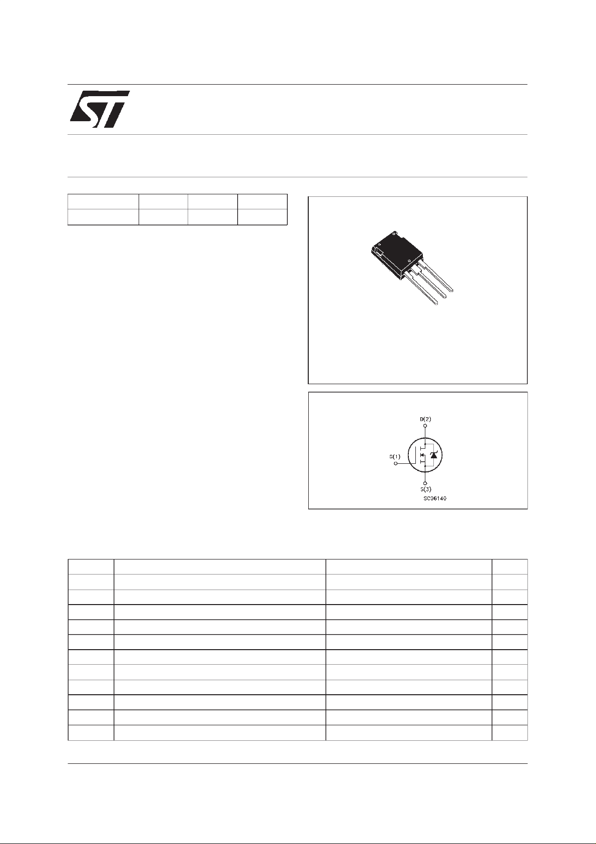
3
2
1
Max247
INTERNAL SCHEMATIC DIAGRAM
ABSOLUTE MAXIMUM RATINGS
Symb o l Parame t er Val u e Uni t
V
V
DGR Drain- gate V oltage (R
V
I
DM
P
dv/dt
T
(•) Pulsewidth limitedby safe operating area (1)ISD≤34 A,di/dt ≤ 200 A/µs, VDD≤ V
June 1998
Drain-s ource Voltage (VGS= 0) 500 V
DS
=20kΩ)
GS
Gate-source Vol t age ± 30 V
GS
I
Drain Curre nt (continuous) at Tc=25oC34A
D
I
Drain Curre nt (continuous) at Tc=100oC 21.4 A
D
500 V
(•) Drain Current (pulsed) 136 A
Total Dissipation at Tc=25oC 450 W
tot
Derat ing Fac t or 3.61 W/
(1) Peak Diode Recovery vo lt age s lope 4.5 V/ns
Stora ge Temperat ure -65 t o 150
stg
T
Max. O perating Junction T em perature 150
j
(BR)DSS,Tj≤TJMAX
o
C
o
C
o
C
1/8
STY34NB50
THERMAL DATA
R
thj-case
R
thj- amb
R
thc-sin k
T
AVALANCHE CHARACTERISTICS
Symb o l Para met er Max Value Uni t
I
AR
E
Ther mal Resistance J unctio n-c ase Max
Ther mal Resistance J unctio n-am bi ent Max
Ther mal Resistance Cas e - si nk Ty p
Maximum Lead Te mperature F or Soldering Pur pose
l
Avalanche Curre nt , Repet it i ve or Not-Repe t it ive
(pulse widt h limite d by T
Singl e Pul se Avalan che Energ y
AS
(starti ng T
=25oC, ID=IAR,VDD=50V)
j
max)
j
0.277
30
0.1
300
34 A
1000 mJ
o
C/W
o
C/W
o
C/W
o
C
ELECTRICAL CHARACTERISTICS (T
=25oC unless otherwisespecified)
case
OFF
Symbol Parameter Test Cond itions Min. Typ. Ma x. Unit
V
(BR)DSS
Drain-source
= 250 µAVGS=0
I
D
500 V
Break dow n V oltage
I
I
DSS
GSS
Zero Gat e Voltage
Drain Curr ent (V
GS
Gat e- bod y Leaka ge
Current (V
DS
=0)
=0)
V
=MaxRating
DS
= Max Rating Tc=125
V
DS
o
C
= ± 30 V
V
GS
10
100
± 100 nA
ON (∗)
Symbol Parameter Test Cond itions Min. Typ. Ma x. Unit
V
GS(th )
R
DS(on)
Gat e Thre shold V oltage
St at i c D r ain -s ource On
V
DS=VGSID
=250µA
VGS=10V ID= 17 A 0.11 0.13 Ω
345V
Resistance
I
D(on)
On St ate Drain Current VDS>I
D(on)xRDS(on)max
34 A
VGS=10V
DYNAMIC
Symbol Parameter Test Cond itions Min. Typ. Ma x. Unit
g
(∗)Forward
fs
Tr ansc on ductance
C
C
C
Input Capacit an c e
iss
Out put Capacitanc e
oss
Reverse Transfer
rss
Capaci ta nc e
VDS>I
D(on)xRDS(on)maxID
=17A 18 20 S
VDS=25V f=1MHz VGS= 0 7000
950
80
9100
1235
104
µA
µA
pF
pF
pF
2/8
STY34NB50
ELECTRICAL CHARACTERISTICS (continued)
SWITCHINGON
Symbol Parameter Test Cond itions Min. Typ. Ma x. Unit
t
d(on)
t
r
Turn-on T ime
Rise Tim e
VDD=250V ID=17A
=4.7 Ω VGS=10V
R
G
46
32
(see test cir c ui t , figure 3)
Q
Q
Q
Tot al Gate Char g e
g
Gate-Source Charge
gs
Gat e- Drain Charge
gd
VDD=400V ID=34A VGS= 10 V 159
35
67
SWITCHINGOFF
Symbol Parameter Test Cond itions Min. Typ. Ma x. Unit
t
r(Voff)
t
t
Off-voltage Rise Time
Fall Time
f
Cross-over T ime
c
VDD=400V ID=34A
=4.7 Ω VGS=10V
R
G
(see test cir c ui t , figure 5)
56
53
120
SOURCE DRAIN DIODE
Symbol Parameter Test Cond itions Min. Typ. Ma x. Unit
I
V
I
SDM
SD
Q
I
RRM
SD
t
Source-drain Current
(•)
Source-drain Current
(pulsed)
(∗) For ward O n Voltage ISD=34A VGS=0 1.6 V
Reverse Recovery
rr
Time
Reverse Recovery
rr
= 34 A di/dt = 100 A/µs
I
SD
=100V Tj= 150oC
V
DD
(see test cir c ui t , figure 5)
950
12
Charge
Reverse Recovery
25
Current
64
45
223 nC
78
74
168
34
136
ns
ns
nC
nC
ns
ns
ns
A
A
ns
µC
A
(∗) Pulsed: Pulse duration = 300 µs, duty cycle 1.5 %
(•) Pulse widthlimited by safe operating area
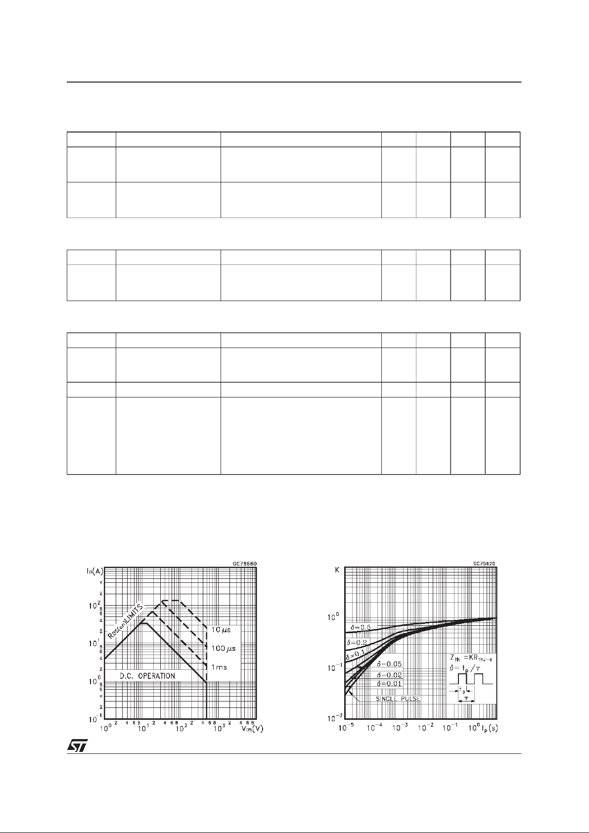
SafeOperating Area ThermalImpedance
3/8

STY34NB50
OutputCharacteristics
Transconductance
TransferCharacteristics
StaticDrain-sourceOn Resistance
Gate Chargevs Gate-sourceVoltage
4/8
CapacitanceVariations

STY34NB50
Normalized Gate Threshold Voltagevs
Temperature
Source-drainDiode ForwardCharacteristics
Normalized On Resistancevs Temperature
5/8

STY34NB50
Fig. 1: Unclamped InductiveLoad TestCircuit
Fig. 3: SwitchingTimes Test Circuits For
ResistiveLoad
Fig. 2: UnclampedInductive Waveform
Fig. 4: Gate Chargetest Circuit
Fig.5: Test CircuitFor InductiveLoad Switching
And DiodeRecovery Times
6/8

Max247 MECHANICAL DATA
STY34NB50
DIM.
MIN. TYP. MAX. MIN. TYP. MAX.
A 4.70 5.30
A1 2.20 2.60
b 1.00 1.40
b1 2.00 2.40
b2 3.00 3.40
c 0.40 0.80
D 19.70 20.30
e 5.35 5.55
E 15.30 15.90
L 14.20 15.20
L1 3.70 4.30
mm inch
P025Q
7/8

STY34NB50
Information furnished isbelieved to be accurate andreliable. However,STMicroelectronics assumes no responsibility for theconsequences
of use of such information nor for any infringement of patents or other rights of third parties which may result from its use. No license is
granted by implication or otherwise under any patent or patent rights of STMicroelectronics. Specification mentioned in this publication are
subject tochange without notice.This publication supersedes and replaces allinformation previously supplied. STMicroelectronics products
are not authorized for use as critical componentsin life support devices or systems withoutexpress written approval of STMicroelectronics.
Australia - Brazil - Canada- China - France- Germany- Italy - Japan- Korea- Malaysia - Malta- Mexico - Morocco- TheNetherlands -
Singapore- Spain - Sweden - Switzerland- Taiwan - Thailand - United Kingdom- U.S.A.
The ST logo isa trademarkof STMicroelectronics
1998STMicroelectronics – Printed in Italy – All Rights Reserved
STMicroelectronicsGROUP OF COMPANIES
.
8/8
 Loading...