

N - CHANNEL ENHANCEMENT MODE
FAST POWER MOS TRANSISTOR
TYPE V
DSS
ST Y30NA50 500 V < 0.175 Ω 30 A
R
DS(on)
I
D
STY30NA50
PRELIMINARY DATA
■ TYPICALR
■ EFFICIENTANDRELIABLEMOUNTING
DS(on)
=0.15 Ω
THROUGH CLIP
■ ± 30V GATE TO SOURCE VOLTAGERATING
■ REPETITIVEAVALANCHETESTED
■ LOW INTRINSIC CAPACITANCE
■ 100% AVALANCHETESTED
■ GATECHARGEMINIMIZED
■ REDUCEDTHRESHOLD VOLTAGESPREAD
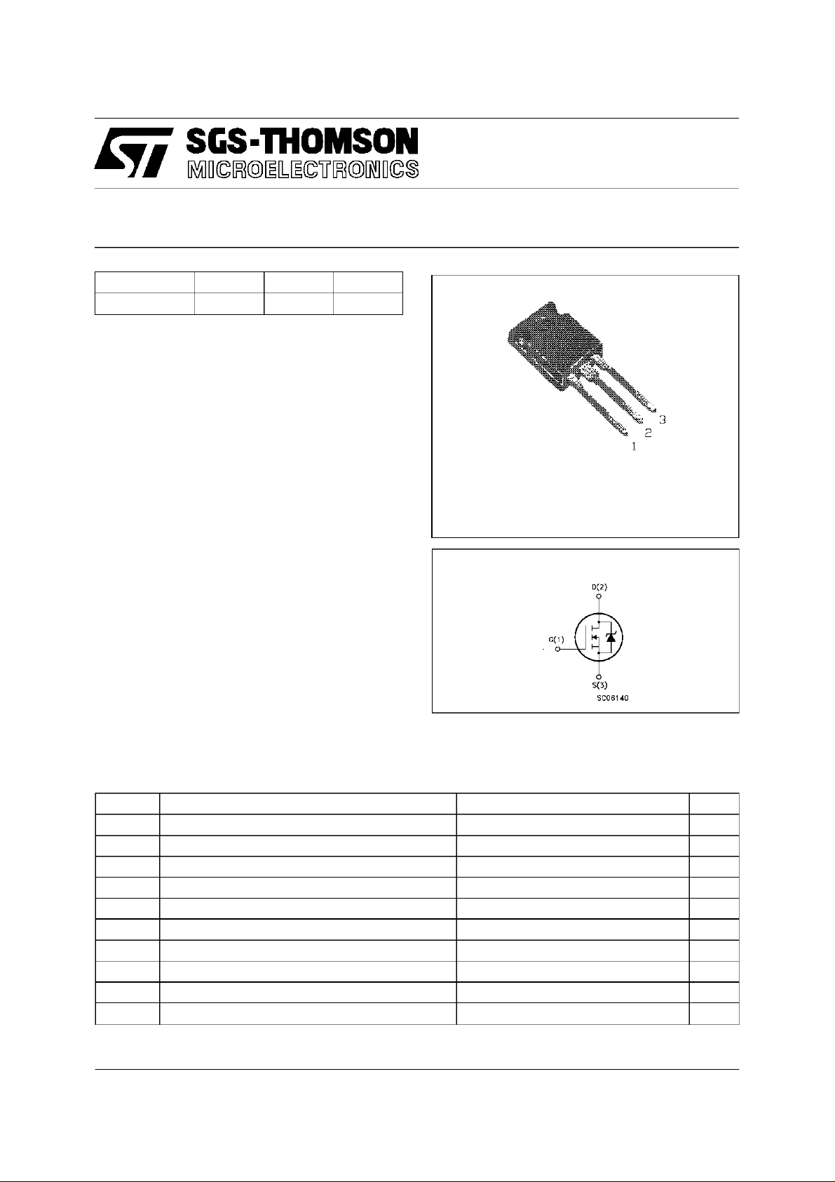
DESCRIPTION
The Max247TMpackage is a new high volume
power pac kage ex ibit ing th e same foot pr int as the
indust ry standar d TO -247, but designed to
accomodate m uch large r silicon chip s , norm ally
supplie d in bigger packages such as TO-26 4. T he
increased die capacity makes t he device ideal to
reduce component count in multiple p aralleled
designs and sav e board space with respect to
larger packages.
APPLICATIONS
■ HIGH CURRENT, HIGH SPEEDSWITCHING
■ SWITCHMODE POWER SUPPLIES (SMPS)
■ DC-ACCONVERTERS FOR WELDING
EQUIPMENTAND UNINTERRUPTIBLE
POWERSUPPLIES (UPS)
Max247
TM
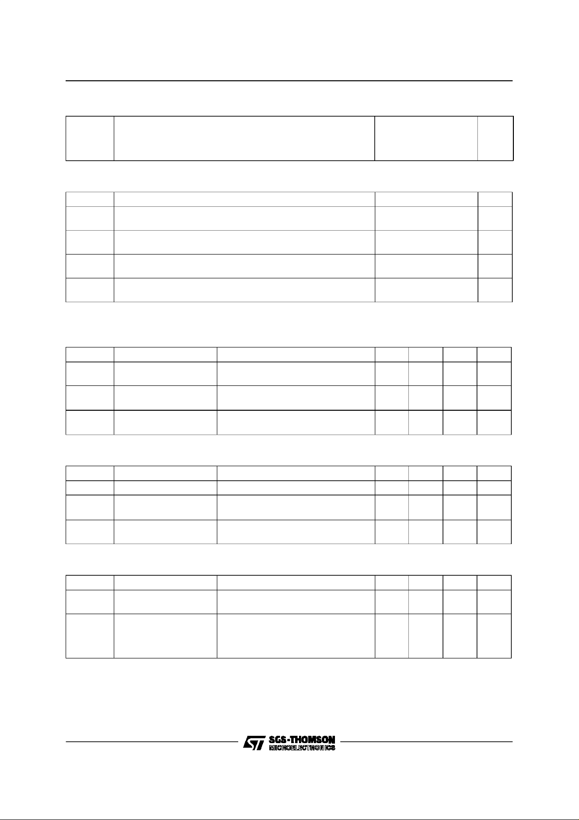
INTERNAL SCHEMATIC DIAGRAM
ABSOLUTE MAXIMUM RATINGS
Symb o l Parame t er Val u e Uni t
V
V
DGR
V
I
DM
P
T
(•) Pulse width limited by safe operating area
March 1996
Drain-source Voltage (VGS= 0) 500 V
DS
Drain- gate Voltage (RGS=20kΩ) 500 V
Gate-sourc e Voltage ± 30 V
GS
I
Drain Current (c ont inuo us) a t Tc=25oC30A
D
I
Drain Current (c ont inuo us) a t Tc=100oC19A
D
(•) Drain Current (puls ed) 120 A
Total Dissipat i on at Tc=25oC 300 W
tot
Derat ing Factor 2.4 W/
Stora ge Temperatu re -55 to 150
stg
T
Max. Operat ing J unct i on T em per at u r e 150
j
o
C
o
C
o
C
1/4
STY30NA50
THERMAL DATA
R
thj-case
R
thj-amb
R
thc-sin k
AVALANCHE CHARACTERISTICS
Symb o l Para met er Max Value Uni t
I
AR
E
E
I
AR
Ther mal Resistance Junct ion-cas e Max
Ther mal Resistance Junct ion-ambient Max
Ther mal Resistance Case-Heats ink Typ
with Conduc t ive Grease
Avalanche Current, Repetit ive or Not-Repetitive
(pulse width lim i t ed by T
Single Pu lse Avalanc he E nerg y
AS
(starti ng T
Repetitive Av alanche Energy
AR
=25oC, ID=IAR,VDD=50V)
j
(pulse width lim i t ed by T
max, δ <1%)
j
max, δ <1%)
j
Avalanche Current, Repetit ive or Not-Repetitive
(T
=100oC, p ulse width limited by Tjmax, δ <1%)
c
0.42
40
0.05
30 A
3000 mJ
180 mJ
19 A
o
C/W
o
C/W
ELECTRICAL CHARACTERISTICS (T
=25oC unlessotherwise specified)
case
OFF
Symbol Parameter Test Condition s Min. Typ. Max. Unit
V
(BR)DSS
Drain-source
ID= 250 µAV
= 0 500 V
GS
Break dow n Voltage
I
I
DSS
GSS
Zero Gate Voltage
Drain Current (V
GS
Gat e- bod y Leaka ge
Current (V
DS
=0)
=0)
V
=MaxRating
DS
=MaxRatingx0.8 Tc= 125oC
V
DS
V
= ± 30 V ± 100 nA
GS
200
1000µAµA
ON (∗)
Symbol Parameter Test Condition s Min. Typ. Max. Unit
V
GS(th )
R
DS(on)
I
D(on)
Gat e Thre shold Volt age VDS=VGSID=250µA2.2533.75V
St at ic Drain-source On
Resistance
VGS=10V ID=15A
=10V ID=15A Tc=100oC
V
GS
On State Drain Current VDS>I
D(on)xRDS(on)max
30 A
0.15 0.175
0.35
VGS=10V
DYNAMIC
Symbol Parameter Test Condition s Min. Typ. Max. Unit
g
(∗)Forward
fs
Tr ansc on ductance
C
C
C
Input Capac it an ce
iss
Out put Capac itance
oss
Reverse Transfer
rss
Capacit a nc e
VDS>I
D(on)xRDS(on)maxID
=15A 25 S
VDS=25V f=1MHz VGS= 0 6150
780
220
8000
1000
290
Ω
Ω
pF
pF
pF
2/4

STY30NA50
ELECTRICAL CHARACTERISTICS (continued)
SWITCHINGON
Symbol Parameter Test Condition s Min. Typ. Max. Unit
t
d(on)
t
(di/dt)
Turn-on Time
Rise Time
r
Tur n-on C urr ent Slope VDD=400V ID=30A
on
VDD=250V ID=15A
=4.7 Ω VGS=10V
R
G
=47 Ω VGS=10V
R
G
40
70
55
90
240 A/ µs
ns
ns
Q
Q
Q
Tot al Gat e Charge
g
Gate-Source Charge
gs
Gat e- Drain Charge
gd
VDD=400V ID=30A VGS= 10 V 245
27
120
320 nC
SWITCHINGOFF
Symbol Parameter Test Condition s Min. Typ. Max. Unit
t
r(Voff)
t
t
Off -voltage Rise Time
Fall T ime
f
Cross-over T im e
c
VDD=400V ID=30A
=4.7 Ω VGS=10V
R
G
75
30
110
100
40
145
SOURCE DRAIN DIODE
Symbol Parameter Test Condition s Min. Typ. Max. Unit
I
SD
I
SDM
V
SD
t
Q
I
RRM
(∗) Pulsed: Pulse duration =300 µs, duty cycle1.5 %
(•) Pulse width limited by safe operating area
Source-drain Current
(•)
Source-drain Current
30
120
(pulsed)
(∗)ForwardOnVoltage ISD=30A VGS=0 1.6 V
Reverse Recovery
rr
Time
Reverse Recovery
rr
ISD=30A di/dt=100A/µs
=100V Tj= 150oC
V
DD
800
17.6
Charge
Reverse Recovery
44
Current
nC
nC
ns
ns
ns
A
A
ns
µC
A
3/4

STY30NA50
Information furnished is believedto be accurate and reliable. However,SGS-THOMSON Microelectronicsassumes no responsability forthe
consequencesof use ofsuch information nor for anyinfringement of patentsor otherrights of third parties which may resultsfrom its use. No
licenseis granted by implicationor otherwise underany patent orpatent rights ofSGS-THOMSONMicroelectronics. Specificationsmentioned
in this publicationare subject to change without notice.This publication supersedes andreplaces all informationpreviouslysupplied.
SGS-THOMSONMicroelectronics productsarenot authorized foruseas criticalcomponents in lifesupportdevices or systems withoutexpress
writtenapproval of SGS-THOMSONMicroelectonics.
1995 SGS-THOMSONMicroelectronics - All RightsReserved
Australia - Brazil - France - Germany- HongKong - Italy- Japan - Korea - Malaysia - Malta- Morocco- The Netherlands-
Singapore- Spain- Sweden- Switzerland- Taiwan - Thailand - United Kingdom - U.S.A
SGS-THOMSONMicroelectronics GROUP OF COMPANIES
...
4/4
 Loading...