

STY140NS10
N-CHANNEL 100V - 0.009 Ω - 140A MAX247 ™
MESH OVERLAY™ POWER MOSFET
TYPE
V
DSS
STY140NS10 100V <0.011
■ TYPICAL R
■ STANDARD THRESHOLD DRIVE
■ 100% AVALANCHE TESTED
(on) = 0.009Ω
DS
R
DS(on)
I
D
140A
Ω
DESCRIPTION
Using the latest high voltage MESH OVERLAY™
process, STMicroe lectronics has desig ned an advanced
family of power MOSFETs with outstanding
performances. The new patent pending strip layout
coupled with the Company’s proprietary edge termination
structure, gives the lowest RDS(on) per area,
exceptional avalanche and dv/dt capabilities and
unrivalled gate charge and switching characteristics.
APPLICATIONS
■ HIGH CURRENT, HIGH SWITCHING SPEED
■ SWITCH MODE POWER SUPPLY (SMPS)
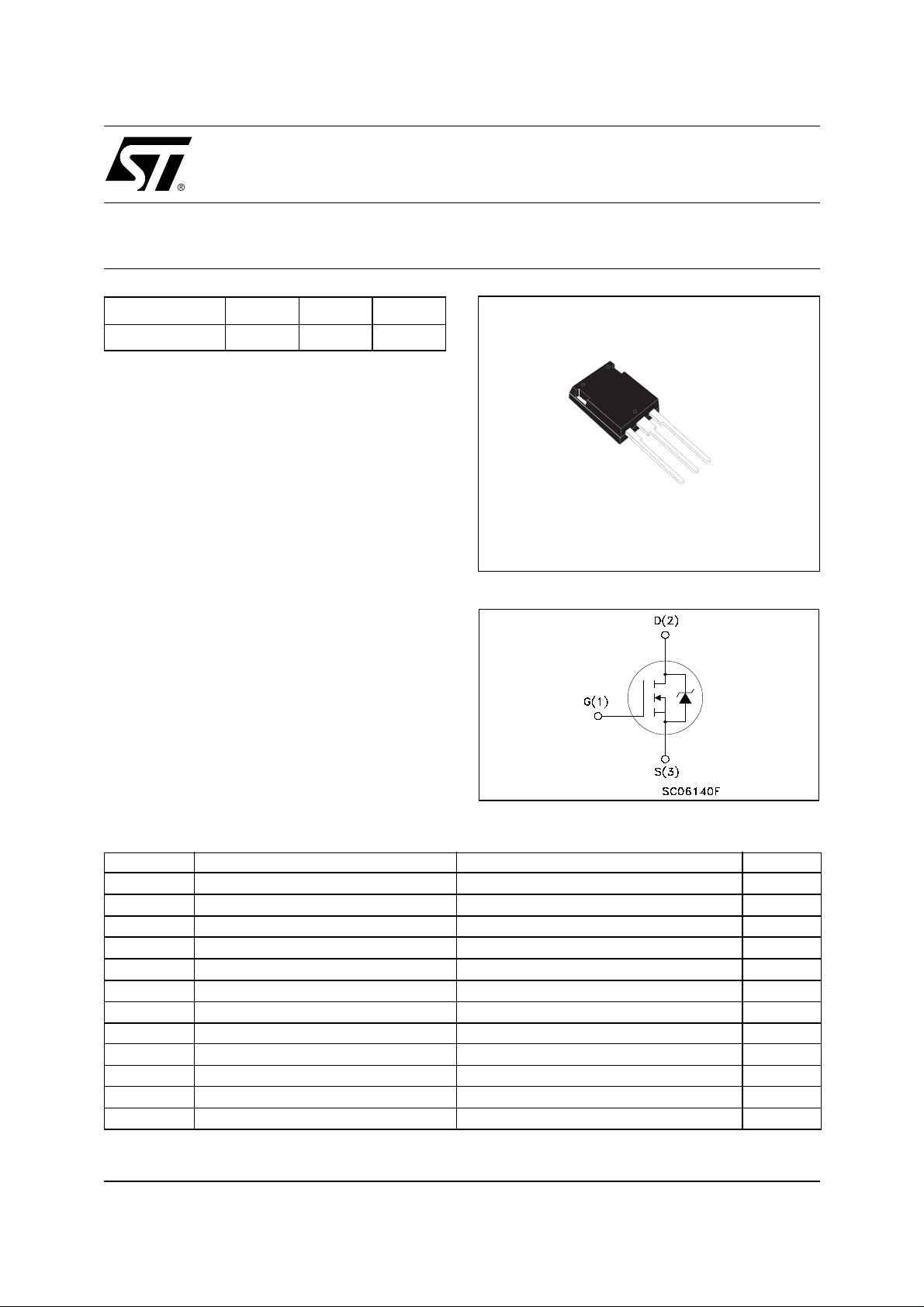
3
2
1
Max247™
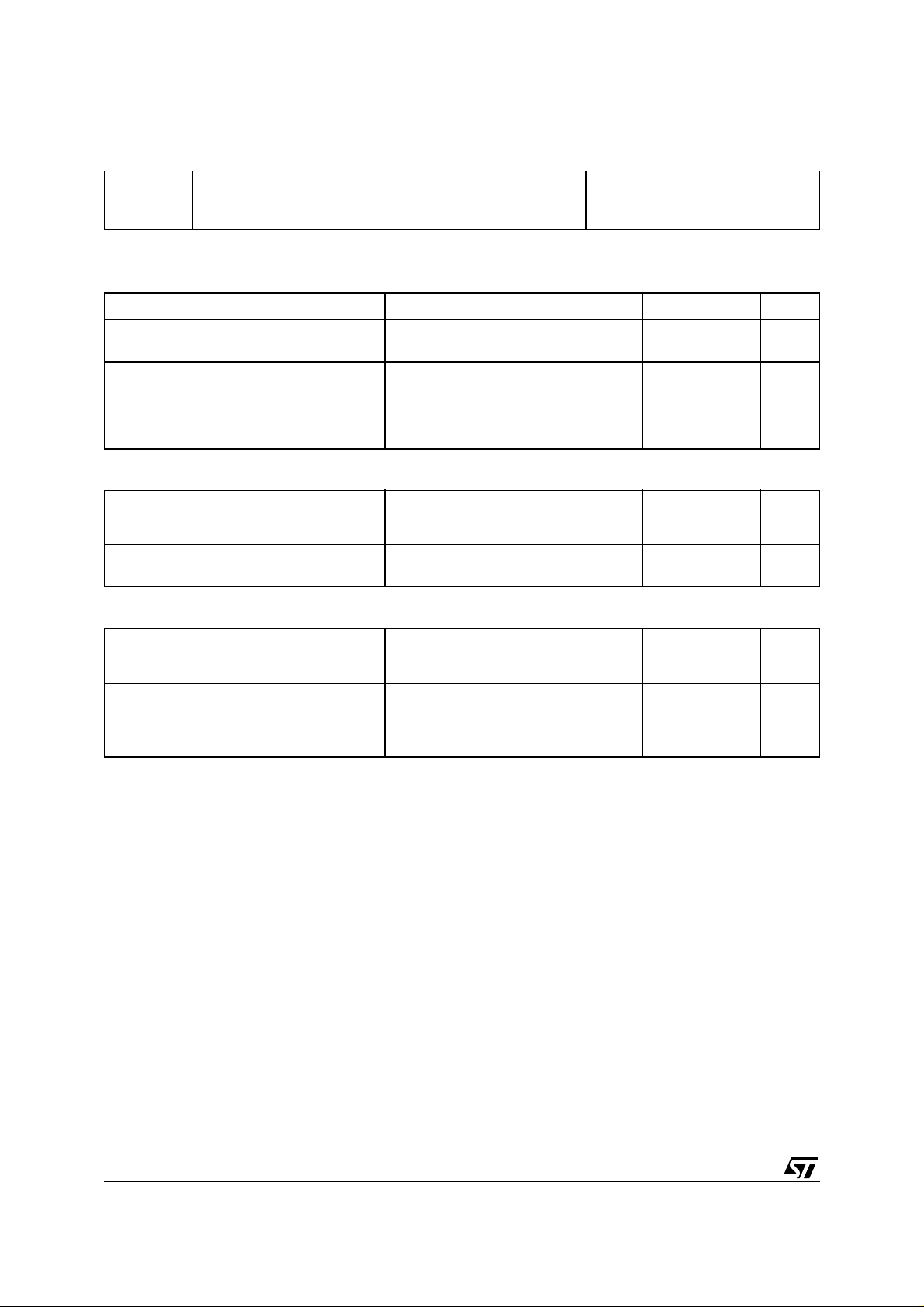
INTERNAL SCHEMATIC DIAGRAM
ABSOLUTE MAXIMUM RATINGS
Symbol Parameter Value Unit
V
DS
V
DGR
V
GS
I
D
I
D
(
I
DM
P
tot
E
AS
dv/dt
T
stg
T
j
(
Pulse width limited by safe operating area. (1) Starting Tj = 25 oC, ID = 70A, VDD= 50V
•)
.
Drain-source Voltage (VGS = 0)
Drain-gate Voltage (RGS = 20 kΩ)
100 V
100 V
Gate- source Voltage ± 20 V
Drain Current (continuos) at TC = 25°C
Drain Current (continuos) at TC = 100°C
•)
Drain Current (pulsed) 560 A
Total Dissipation at TC = 25°C
140 A
99 A
450 W
Derating Factor 3 W/°C
(1)
Single Pulse Avalanche Energy 2900 mJ
(2)
Peak Diode Recovery voltage slope 5 V/ns
Storage Temperature -55 to 175 °C
Operating Junction Temperature -55 to 175 °C
(2) I
≤140A, di/dt ≤200A/µs, VDD ≤ V
SD
(BR)DSS
, Tj ≤ T
JMAX.
1/8August 2001
STY140NS10
THERMA L D ATA
Rthj-case
Rthj-amb
T
Thermal Resistance Junction-case
Thermal Resistance Junction-ambient
Maximum Lead Temperature For Soldering Purpose
j
Max
Max
Typ
0.33
30
300
°C/W
°C/W
°C
ELECTRICAL CHARACTERISTICS (T
= 25 °C unless otherwise specified)
case
OFF
Symbol Parameter Test Conditions Min. Typ. Max. Unit
I
V
(BR)DSS
Drain-source Breakdown
= 250 µA, VGS = 0
D
100 V
Voltage
V
= Max Rating
DS
V
= Max Rating TC = 125°C
DS
V
= ± 20V
GS
1
10
±100 nA
ON
(1)
I
DSS
I
GSS
Zero Gate Voltage
Drain Current (V
GS
Gate-body Leakage
Current (V
DS
= 0)
= 0)
Symbol Parameter Test Conditions Min. Typ. Max. Unit
V
GS(th)
R
DS(on)
Gate Threshold Voltage
Static Drain-source On
= VGS I
DS
V
= 10 V ID = 70 A
GS
= 250 µA
D
24V
0.009 0.011
V
Resistance
DYNAMIC
Symbol Parameter Test Conditions Min. Typ. Max. Unit
(*)
g
fs
C
iss
C
oss
C
rss
Forward Transconductance
Input Capacitance
Output Capacitance
Reverse Transfer
Capacitance
V
= 20 V ID= 70 A
DS
= 25V, f = 1 MHz, VGS = 0
V
DS
50 S
12600
2100
690
µA
µA
Ω
pF
pF
pF
2/8

STY140NS10
ELECTRICAL CHARACTERISTICS (continued)
SWITCHING ON
Symbol Parameter Test Conditions Min. Typ. Max. Unit
= 50 V ID = 70 A
t
d(on)
Turn-on Delay Time
t
r
Rise Time
V
DD
R
= 4.7 Ω VGS = 10 V
G
(Resistive Load, Figure 1)
Q
g
Q
gs
Q
gd
Total Gate Charge
Gate-Source Charge
Gate-Drain Charge
=50V ID=140A VGS=10V
V
DD
(see test circuit, Figure 2)
SWITCHING OFF
Symbol Parameter Test Conditions Min. Typ. Max. Unit
= 50 V ID = 70 A
t
d(off)
Turn-off Delay Time
t
f
Fall Time
V
DD
R
= 4.7Ω, V
G
GS
= 10 V
(Resistive Load, Figure 1)
SOURCE DRAIN DIODE
Symbol Parameter Test Conditions Min. Typ. Max. Unit
I
SD
I
SDM
V
SD
t
rr
Q
rr
I
RRM
(*)
Pulsed: P ul se duration = 300 µs, duty cycle 1.5 %.
(
•)Pulse width limited by s afe operating area.
Source-drain Current
(•)
Source-drain Current (pulsed)
(*)
Forward On Voltage
Reverse Recovery Time
Reverse Recovery Charge
Reverse Recovery Current
I
= 140 A VGS = 0
SD
= 140 A di/dt = 100A/µs
I
SD
V
= 20 V Tj = 150°C
r
(Inductive Load, Figure 3)
40
150
450
70
170
465
270
600 nC
140
560
1.5 V
275
2
15
ns
ns
nC
nC
ns
ns
A
A
ns
µ
A
C
Safe Operating Area Thermal Impedance
3/8

STY140NS10
Output Characteristics Transfer Characteristics
Transconductance Static Drain-source On Resistance
Gate Charge vs Gate-source Voltage Capacitance Variations
4/8

STY140NS10
Normalized Gate Threshold Voltage vs Temperature Normalized on Resistance vs Temperature
Source-drain Diode Forward Characteristics Normalized Breakdown Voltage vs Temperature
. .
5/8

STY140NS10
Fig. 1: Switching Times Test Circuits For Resistive
Load
Fig. 3: Test Circuit For Diode Recovery Behaviour
Fig. 2: Gate Charge test Circuit
6/8

Max247 MECHANI CAL DATA
STY140NS10
DIM.
MIN. TYP. MAX. MIN. TYP. MAX.
A 4.70 5.30
A1 2.20 2.60
b 1.00 1.40
b1 2.00 2.40
b2 3.00 3.40
c 0.40 0.80
D 19.70 20.30
e 5.35 5.55
E 15.30 15.90
L 14.20 15.20
L1 3.70 4.30
mm inch
P025Q
7/8

STY140NS10
Information furnished is believed to be accurate and reliable. However, STM ic roelectronics assumes no responsi bility for the consequ ences
of use of such information nor for any infringement of patents or other rights of third parties which may result from its use. No license is granted
by implic ation or o th erwise under any patent or patent rights of STMi croelectronics. Sp ecifications menti oned in thi s publication are subject
to change without notice. This publication supersedes and replaces all information previously supplied. STMicroelectronics products are not
authorized for use as cri tical comp onents in lif e support dev i ces or systems wi thout exp ress written approval of STMicroel ectronics.
The ST log o i s registered trademark of STMicroelectronics
2001 STMi croelectronics - All Ri ghts Reserved
All other names are the property of their respective ow ners.
Australi a - Brazil - Ch i na - Finland - F rance - Germ any - Hong Kong - India - Italy - Japan - Malaysia - Mal t a - Morocc o -
Singapor e - Spain - Sweden - Switz erl and - United Kingdom - U.S.A.
STMicroelect ro n ics GRO UP OF COMPANI ES
http://www.st.com
8/8
 Loading...