

STTA1212D
TURBOSWITCH
ULTRA-FASTHIGH VOLTAGE DIODE
MAINPRODUCTCHARACTERISTICS
I
F(AV)
V
RRM
(typ) 50 ns
t
rr
(max) 2.0 V
V
F
12A
1200V
FEATURESAND BENEFITS
ULTRA-FAST,SOFT RECOVERY.
VERY LOW OVERALL POWER LOSSES IN
BOTH THE DIODE AND THE COMPANION
TRANSISTOR.
HIGHFREQUENCYAND/ORHIGHPULSED
CURRENTOPERATION.
HIGHREVERSEVOLTAGECAPABILITY.
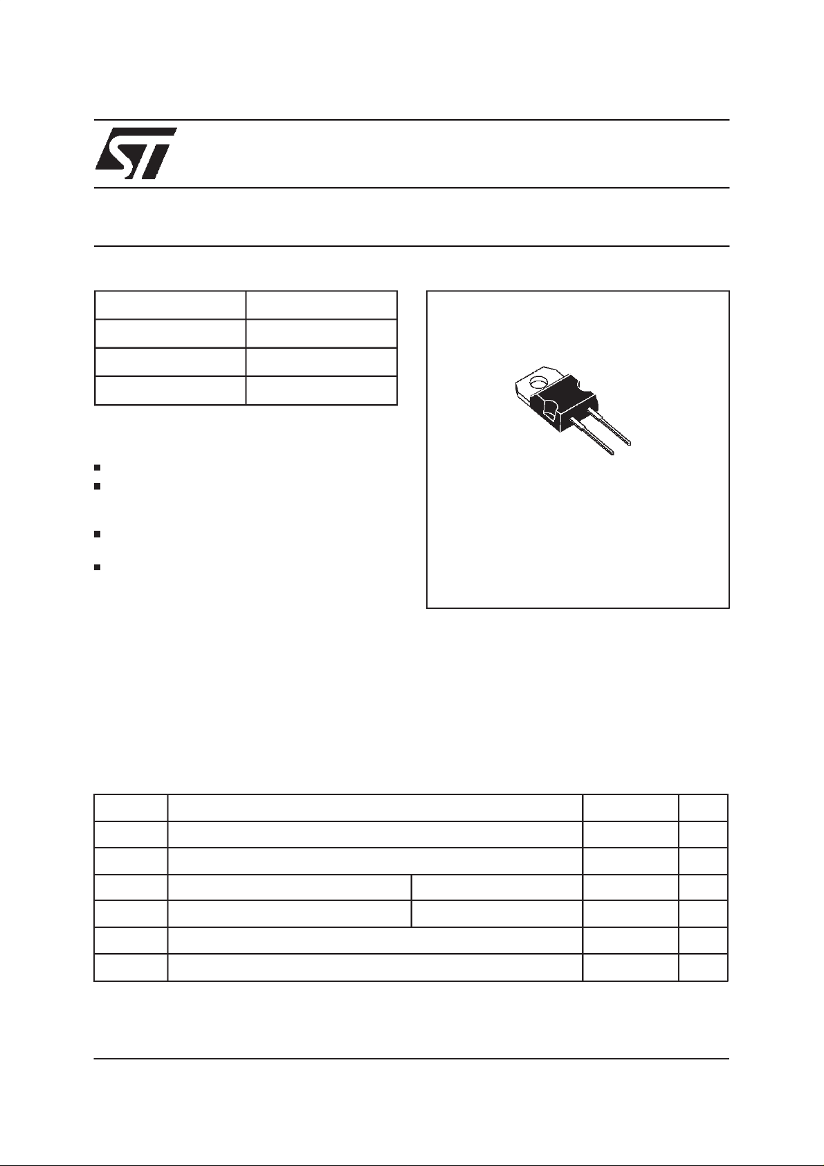
DESCRIPTION
K
TO-220AC
A
K
TURBOSWITCH 1200V drastically cuts losses in
allhighvoltageoperationswhich require extremely
fast,soft andnoise-freepower diodes.Due to their
optimizedswitchingperformancesthey alsohighly
decrease power losses in any associated
They are particularly suitable in motor control
circuitries, or in the primaryof SMPS as snubber,
clampingor demagnetizingdiodes. They are also
suitable for secondary of SMPS as high voltage
rectifierdiodes.
switchingIGBT or MOSFET in all freewheelmode
operations.
ABSOLUTE RATINGS(limitingvalues)
Symbol Parameter Value Unit
V
RRM
I
F(RMS)
I
FRM
I
FSM
T
stg
T
j
TURBOSWITCH is a trademark of STMicroelectronics
November 1999 - Ed:5B
Repetitivepeakreverse voltage 1200 V
RMS forward current 30 A
Repetitivepeakforward current tp = 5 µs F= 5kHzsquare 160 A
Surge non repetitive forward current tp = 10ms sinusoidal 100 A
Storagetemperaturerange - 65 to +150 °C
Maximumoperatingjunction temperature 150 °C
1/8

STTA1212D
THERMALAND POWERDATA
Symbol Parameter Test conditions Value Unit
R
th(j-c)
P
1
Junctionto case thermalresistance 1.9 °C/W
Conductionpowerdissipation I
=12Aδ=0.5
F(AV)
29.2 W
Tc= 95°C
P
max
Total power dissipation
Tc= 89°C 32.1 W
Pmax= P1+ P3 (P3 = 10%P1)
STATICELECTRICAL CHARACTERISTICS
Symbol Parameter Test conditions Min Typ Max Unit
V
I
R**
F*
Forwardvoltagedrop IF=12A Tj = 25°C
Reverseleakage current VR=0.8x
V
RRM
Vto Thresholdvoltage Ip <3.I
Tj = 125°C 1.35
Tj=25°C
Tj = 125°C 0.8
Tj = 125°C 1.57 V
F(AV)
2.2
2.0
100
5.0
Rd Dynamicresistance 36 m
Test pulses : * tp = 380 µs, δ <2%
** tp= 5ms ,δ<2%
Toevaluatethe maximum conductionlossesuse the followingequation :
P=V
toxIF(AV)
+RdxI
F2(RMS)
DYNAMICELECTRICAL CHARACTERISTICS
V
V
µ
mA
A
Ω
TURN-OFF SWITCHING
Symbol Parameter Testconditions Min Typ Max Unit
S
t
rr
I
RM
factor
Reverserecovery
time
Maximumreverse
recoverycurrent
Tj = 25°C
I
=0.5 A IR= 1A Irr = 0.25A
F
=1A dIF/dt=-50A/µsVR=30V
I
F
Tj = 125°C VR= 600V IF=12A
/dt= -96A/µs
dI
F
dI
/dt= -500A/µs30
F
Softnessfactor Tj = 125°CVR=600V IF=12A
dI
/dt= -500A/µs 1.2
F
50
100
18
TURN-ON SWITCHING
Symbol Parameter Testconditions Min Typ Max Unit
t
fr
V
Fp
Forwardrecoverytime Tj = 25°C
=12A, dIF/dt = 96 A/µs
I
F
measuredat 1.1 × V
Peakforwardvoltage Tj = 25°C
=12A,dIF/dt = 96 A/µs
I
F
I
=40A,dIF/dt = 500A/µs40
F
max
F
900
30
ns
A
/
ns
V
2/8
STTA1212D
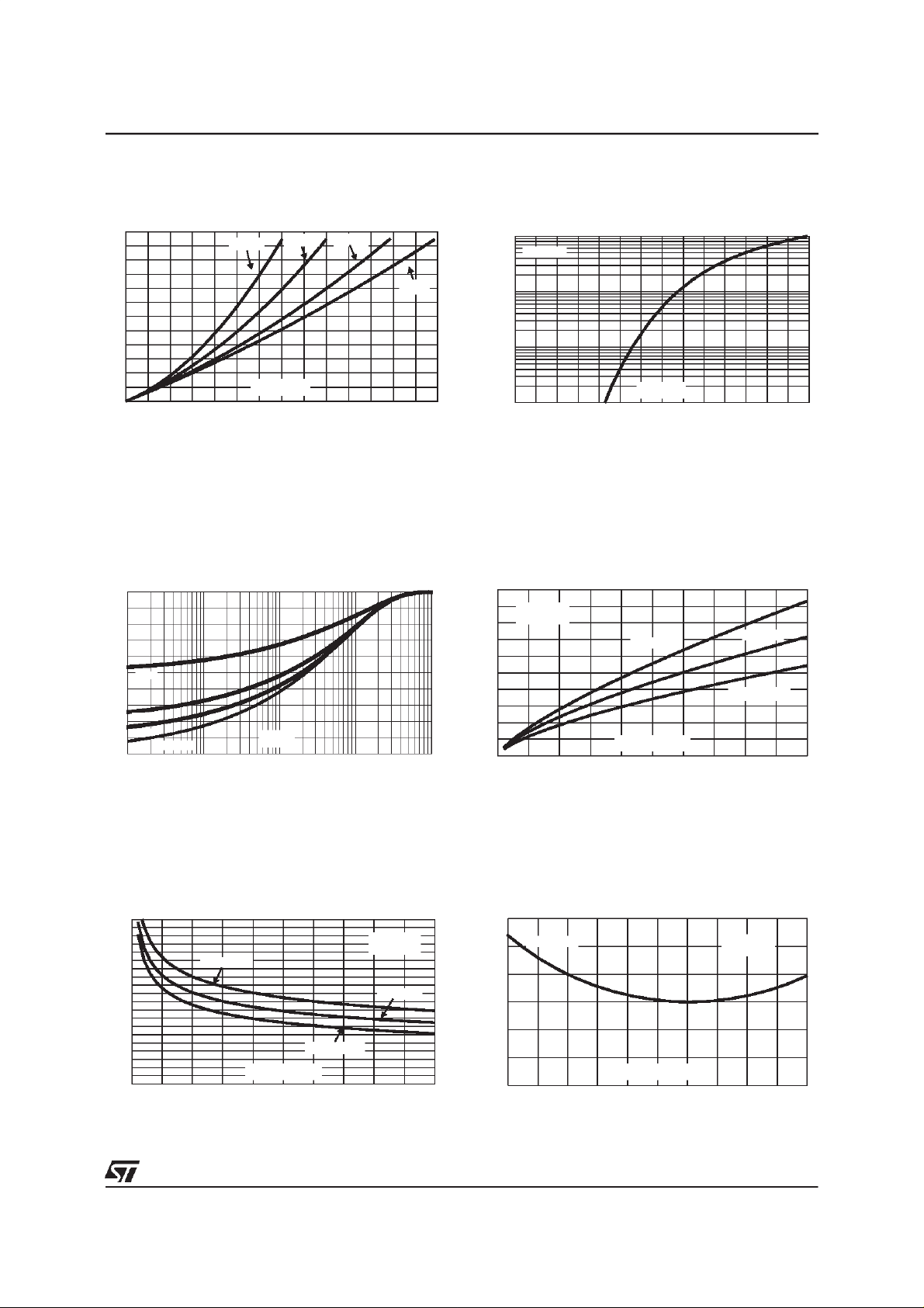
Fig.1: Conductionlosses versusaveragecurrent.
P1(W)
30
δ = 0.1
δ= 0.5δ = 0.2
25
20
δ =1
15
10
5
IF(av) (A)
0
0 2 4 6 8 10 12 14
Fig. 3: Relative variation of thermal impedance
junctionto case versuspulse duration.
Zth(j-c)/Rth(j-c)
1.0
0.8
0.6
δ = 0.5
0.4
δ = 0.2
0.2
δ = 0.1
0.0
Single pulse
1E-4 1E-3 1E-2 1E-1 1E+0
tp(s)
Fig. 2: Forward voltage drop versus forward cur-
rent(maximumvalues).
IFM(A)
100.0
Tj=125°C
10.0
1.0
VFM(V)
0.1
0.0 0.5 1.0 1.5 2.0 2.5 3.0 3.5
Fig. 4: Peak reverse recovery current versus
dI
/dt(90% confidence).
F
IRM(A)
50
VR=600V
Tj=125°C
40
30
IF=2*IF(av)
20
10
dIF/dt(A/µs)
0
0 100 200 300 400 500
IF=IF(av)
IF=0.5*IF(av)
Fig. 5: Reverse recovery time versus dIF/dt (90%
confidence).
trr(ns)
500
450
400
350
IF=2*IF(av)
300
250
200
150
100
50
0
0 100 200 300 400 500
dIF/dt(A/µs)
IF=0.5*IF(av)
VR=600V
Tj=125°C
IF=IF(av)
Fig.6: Softnessfactor (tb/ta) versusdIF/dt(typical
values).
S factor
1.40
IF<2*IF(av)
1.20
1.00
dIF/dt(A/µs)
0.80
0 100 200 300 400 500
VR=600V
Tj=125°C
3/8

STTA1212D
Fig. 7: Relative variationof dynamic parameters
versusjunctiontemperature(referenceTj=125°C).
1.1
1.0
0.9
0.8
0.7
25 50 75 100 125
S factor
IRM
Tj(°C)
Fig. 9: Forward recovery time versus dIF/dt (90%
confidence).
tfr(ns)
600
VFR=1.1*VF max.
500
IF=IF(av)
Tj=125°C
Fig. 8: Transient peak forward voltage versus
dI
/dt(90% confidence).
F
VFP(V)
70
IF=IF(av)
60
Tj=125°C
50
40
30
20
10
0
0 100 200 300 400 500
dIF/dt(A/µs)
400
300
200
dIF/dt(A/µs)
100
0 100 200 300 400 500
4/8

APPLICATIONDATA
The 1200V TURBOSWITCH series has been
designed to provide the lowest overall power
losses in all high frequencyor high pulsed current
operations. In such applications (Fig A to D),the
wayof calculatingthe powerlossesis givenbelow:
TOTALLOSSES
due to the diode
P = P1+ P2+ P3+ P4+ P5 Watts
STTA1212D
CONDUCTION
LOSSES
in thediode
Fig.A : ”FREEWHEEL”MODE.
SWITCHING
TRANSISTOR
V
R
tp
REVERSE
LOSSES
in thediode
T
SWITCHING
LOSSES
in the diode
DIODE:
TURBOSWITCH
SWITCHING
LOSSES
in the tansistor
due to the diode
IL
F=1/T δ= tp/T
LOAD
5/8

STTA1212D
Fig. B : SNUBBERDIODE. Fig. C : DEMAGNETIZINGDIODE.
PWM
tp
T
F=1/T δ= tp/T
Fig.D : RECTIFIERDIODE.
STATIC& DYNAMIC CHARACTERISTICS . POWERLOSSES .
Fig. E: STATICCHARACTERISTICS
6/8
I
I
F
Rd
V
R
V
to
V
F
V
I
R
Conductionlosses :
P1 = V
t0.IF(AV)+Rd.IF2(RMS)
Reverse losses:
P2 = V
R.IR
.(1-δ)

APPLICATIONDATA (Cont’d)
Fig.F: TURN-OFFCHARACTERISTICS
STTA1212D
V
I
I
dI /dt
V
I
RM
I
V
trr = ta + tb
S = tb/ta
TRANSISTOR
F
DIODE
tbta
dI /dt
R
trr = ta + tb S = tb / ta
dIF/dt = VR/L
RECTIFIER
OPERATION
tbta
dI /dt
I
RM
R
IL
t
VR
V
Turn-onlosses:
(inthe transistor,due to the diode)
2
×
I
I
RM
RM
× ( 3 + 2 ×
6
xdI
I
×
× (S+2) ×
L
2
x
dI
F
F
dt
⁄
S)×F
dt
⁄
F
P5=
+
V
R
V
×
R
Turn-offlosses (in the diode) :
2
I
×
RM
6
xdI
×
⁄
F
S×F
dt
t
P3=
V
R
Turn-offlosses :
(withnon negligibleserial inductance)
2
I
V
t
R
P3’=
×
R
RM
6
xdI
×
I
L
RM
S×F
×
dt
⁄
F
2
F
×
+
2
P3,P3’andP5are suitablefor powerMOSFETand
IGBT
Fig. G: TURN-ONCHARACTERISTICS
I
F
I
dI /dt
F
0
V
F
V
Fp
1.1V
F
0t
tfr
Fmax
t
Turn-onlosses:
P4= 0.4 (V
V
F
FP-VF
).I
Fmax.tfr
.F
7/8

STTA1212D
PACKAGEDATA
TO-220AC (JEDECoutline)
H2
ØI
L2
L9
F1
F
G
L5
L6
L4
DIMENSIONS
REF.
A
C
A 4.40 4.60 0.173 0.181
Millimeters Inches
Min. Max. Min. Max.
C 1.23 1.32 0.048 0.051
L7
D 2.40 2.72 0.094 0.107
E 0.49 0.70 0.019 0.027
F 0.61 0.88 0.024 0.034
F1 1.14 1.70 0.044 0.066
D
G 4.95 5.15 0.194 0.202
H2 10.00 10.40 0.393 0.409
L2 16.40 typ. 0.645typ.
L4 13.00 14.00 0.511 0.551
M
E
L5 2.65 2.95 0.104 0.116
L6 15.25 15.75 0.600 0.620
L7 6.20 6.60 0.244 0.259
L9 3.50 3.93 0.137 0.154
M 2.6 typ. 0.102 typ.
Diam.I 3.75 3.85 0.147 0.151
Orderingtype Marking Package Weight Base qty Delivery mode
STTA1212D STTA1212D TO-220AC 1.86g 50 Tube
Coolingmethod:by conduction(C)
Recommendedtorque value: 0.55 N.m.
Maximumtorquevalue:0.70 N.m.
Epoxymeets UL94,V0
Informationfurnished is believed to beaccurate and reliable.However,STMicroelectronics assumes no responsibilityforthe consequences of
use ofsuch information nor forany infringement of patents or other rightsof third parties which mayresultfrom itsuse. No license is grantedby
implication or otherwise under any patent or patent rights of STMicroelectronics. Specifications mentioned in this publication are subject to
change without notice. This publication supersedes and replaces all information previously supplied.
STMicroelectronics products are not authorized for use as critical components in life supportdevices or systems without express writtenapproval of STMicroelectronics.
The ST logo is a registered trademark of STMicroelectronics
1999 STMicroelectronics - Printedin Italy- All rights reserved.
STMicroelectronics GROUP OF COMPANIES
Australia - Brazil - China - Finland - France - Germany - Hong Kong - India - Italy -Japan - Malaysia
Malta - Morocco - Singapore - Spain - Sweden - Switzerland - United Kingdom - U.S.A.
http://www.st.com
8/8
 Loading...